

SUBSCRIBERLINEINTERFACEKIT
. PROGRAMMABLEDC FEEDINGRESIS-TAN-
CEANDLIMITINGCURRENT(fourvaluesavailable)
.THREEOPERATING MODES:
STAND-BY,CONVERSATION,RINGING
.NORMAL/BOOSTBATTERY,DIRECT/REVER-
SEPOLARITY
.SIGNALLINGFUNCTION(off-hook/GND-key)
.
FILTERED OFF-HOOK DETECTION IN
STAND-BY(10ms)
.QUICK OFF-HOOKDETECTION IN CONVER-
SATION (< 1ms) FOR LOW DIAL PULSE DETECTIONDISTORTION
.
HYBRIDFUNCTION
.RINGING GENERATION WITH QUASI ZERO
OUTPUT IMPEDANCE, ZERO CROSSINGINJECTION (no ext. relay needed) AND RING
TRIPDETECTION
.AUTOMATIC RINGING STOP WHEN OFF-
HOOKIS DETECTED
.
PARALLEL AND SERIAL DIGITAL INTERFACES
.
TELETAXESIGNALINJECTION(2V
RMS
/5V
RMS
.LOW NUMBER OF EXTERNAL COMPO-
NENTS
.GOODREJECTION OF THE NOISEON BAT-
TERY VOLTAGE (20dB at 10Hz and 35dB at
1kHz)
.POSSIBILITY TO WORK ALSO WITH HIGH
COMMONMODE CURRENTS
.INTEGRATEDTHERMAL PROTECTIONWITH
THERMALOVERLOADINDICATION
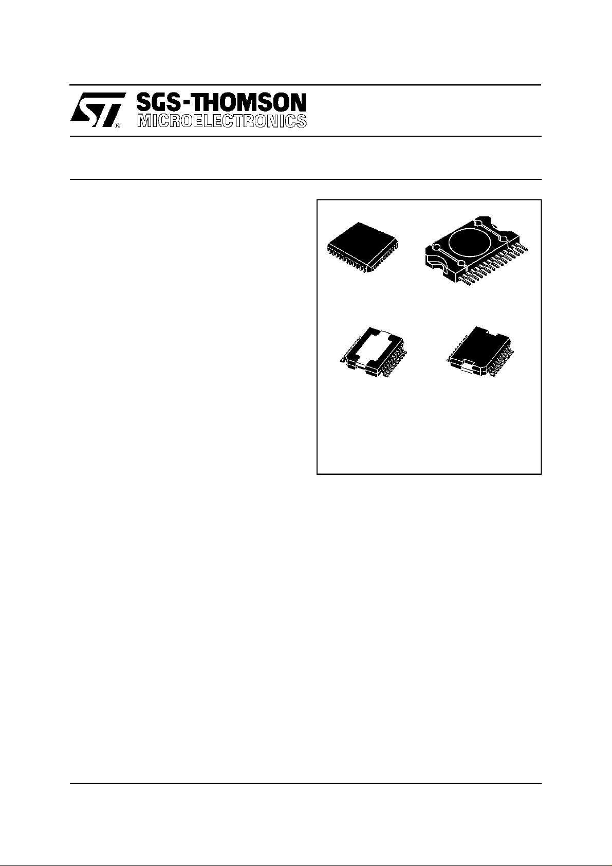
.SURFACEMOUNTPACKAGE
(PLCC44+ PowerSO-20)
DESCRIP TION
The ST SLIC KIT (L3000S/L3030)is a set of solid
statedevicesdesignedto integratemainof the functionsneeded to interfacea telephoneline.It consists of 2 integrated devices : the L3000S line
interfacecircuit and the L3030controlunit.
Thiskit performsthemainfeaturesof theBORSHT
functions:
Batteryfeed
-
Ringing
-
Signalling
-
Hybrid
-
L3000S
L3030
PREL IMINAR Y DATA
PLCC44 FLEXIWATT15
PowerSO20
slug-up slug-down
ORDERING NUMBERS :
L3030 (PLCC44)
L3000SX-VM (FLEXIWATT15)
)
Additionalfunctions,such asbatteryreversal,extra
batteryuse,lineovervoltagesensingandmeteringpulse injection are also featured ; most external
characteristics,asACandDCimpedances,areprogrammablewithexternalcomponents.The SLICinjectsringing inbalancedmodeandfor that,as well
as for the operation in battery boosted, a positive
batteryvoltageshall be availableon thesubscriber
card.Asthe rightringingsignalamplificationbothin
voltageandin currentis providedby SLIC, thering
signalgeneratorshallonlyprovidea lowlevelsignal
(0.285Vrms).
Thiskitisfabricatedusinga 140VBipolartechnologyforL3000Sand a 12VBipolar I
L3030.
L3030 is available PLCC44 and L3000S in both
FLEXIWATT15andPowerSO-20forsurfacemount
application.
Thiskit is suitableforallthe followingapplications:
C.O.(CentralOffice),DLC(DigitalLoopCarrier)and
high range PABX (Private Automatic Branch Exchange).
L3000SX (PowerSO20 slug-up)
L3000SX-77(PowerSO20slug-down)
2
L technologyfor
June 1997
1/29

L3000S - L3030
PIN C O NNE CTIONS (top view)
V
N.C.
TIP
MNT
V
BGND
V
DD
V
V
BIM
V
PLCC44
V
B-
1
2
3
4
B+
5
6
7
IN
8
9
B-
10
D97TL290
20
19
18
17
16
15
14
13
12
11
V
B-
RING
N.C.
IL
IT
C2
C1
REF
AGND
V
B-
B-
V
BIM
V
IN
V
DD
BGND
V
B+
MNT
TIP
N.C. RING
V
B-
10
9
8
7
6
5
4
3
2
1
PowerSO-20(slug-down)
FLEXIWATT15
D94TL125
PowerSO-20(slug-up)
11
12
13
14
15
16
17
18
19
20
V
B-
AGND
REF
C1
C2
IT
IL
N.C.
V
B-
2/29

L3000S - L3030
PIN DESCRIPTION(L3000S)
FLEX.
N
10 13 REF Voltage reference output with very low temperature coefficient. The connected resistor
11 14 C1 Digital signal input (3 levels) that defines device status with pin 12.
12 15 C2 Digital signal input (3 levels) that defines device status with pin 11.
13 16 I
14 17 I
15 19 RING B line termination output with current capability up to 100mA (I
PSO
°
1 3 TIP A line termination output with current capabilityup to 100mA (I
Name Description
N
°
from this pin).
is the current sourced
a
2 4 MNT Positive Supply Voltage Monitor
35V
4 6 BGND Battery ground relative to the V
57V
+ Positive Battery Supply Voltage
B
+ and the VB– supply voltages.
It is also the reference ground for TIP and RING signals.
Positive Power Supply + 5V
DD
B
6 8 VIN 2 wire unbalanced voltage input.
7 9 VBIM Output voltage without current capability, with the following functions :
- give an image of the total battery voltage scaled by 40 to the low voltage part.
- filter by an external capacitor the noise on V
81,10
11, 20
V
– Negative Battery Supply Voltage
B
9 12 AGND Analog Ground. All input signals and the V
–.
B
supply voltage must be referred to this pin.
DD
sets internal circuit bias current.
High precision scaled transversal line current signal.
T
L
I
+ I
a
IT=
b
100
Scaled longitudinal line current signal.
I
− I
b
IL=
a
100
this pin).
is the current sunk into
b
– 2, 18 N.C. Not connected
Notes: 1) Unless otherwisespecified all the diagrams in this datasheet refers to the FLEXIWATT15 pin connection.
2) All informations relative to the PowerSO-20 package option should be considered as advanced information on a new product
now in development or undergoing evaluation. Details are subject to change without notice.
3/29

L3000S - L3030
PIN DESCRIPTION(L3030)
Pin Symbol Function
1 TST This pin is connected internally for test purpose. It should not be used as a tie point for
2 REF Bias Set
3 AGND Analog Ground
4 VSS – 5V
5 VDD + 5V
6 N.C. Not connected.
7 CZS AC Feedback Input
8 ACF AC Line Impedance Synthesis
9 ZAC AC Impedance Adjustement
10
11
12
13 VOUT Two wire unbalanced output.
14 CM Capacitor Multiplier Input
15 RC DC Feedback Input
16 IT Transversal Line Current
17 RDC DC Feeding System
18 EIA Read/write Command
19 NCS Chip Select Command
20 DIO Data Input/output
21 DCKL Clock Signal
22 DGND Digital Ground
23 N.C. Not connected.
24 N.C. Not connected.
25 N.C. Not connected.
26 CI Input/output Changing Command
27 C1 State Control Signal 1
28 C2 State Control Signal 2
29 N.C. Not connected.
30 N.C. Not connected.
31 IL Longitudinal Line Current
32 CRTS Ringtrip Det. & TTX Shaping
33 TTXIN Teletaxe Signal Input
34 RGTTX TTX Filter Level Compensation
35 TTXF TTX Filter Input
36 ZB Balancing Network
37
38
39
40 TX 4W Sending Output
41 RX/RG 4W Receiving and Ring Input
42 VBIM Battery Image Input
43
44
TST
TST
TST
external components.
These pins are connected internally for test purpose. It should not be used as a tie point
for external components.
These pins are connected internally for test purpose. It should not be used as a tie point
for external components.
These pins are connected internally for test purpose. It should not be used as a tie point
for external components.
4/29

L3000S BLOCK DIAGRAM
L3000S - L3030
L3030 BLOCK DIAGRAM
5/29
L3000S - L3030
ABSOLUTE MAXIMUM RATINGS
Symbol Parameter Value Unit
V
– Negative Battery Voltage – 80 V
b
V
+ Positive Battery Voltage 80 V
b
|V
–| + |Vb+| Total Battery Voltage 140 V
b
V
dd
V
ss
V
agnd–Vbgnd
T
j
T
stg
THERMAL DATA
Symbol Parameter Value Unit
L3000S HIGH VOLTAGE Flexiwatt PWSO20
R
th j-case
R
th j-amb
L3030 LOW VOLTAGE
R
th j-amb
OPERATINGRANGE
Symbol Parameter Min. Typ. Max. Unit
T
oper
– Negative Battery Voltage – 70 – 48 – 24 V
V
b
V
+ Positive Battery Voltage 0 + 72 + 75 V
b
V
–+Vb+ Total Battery Voltage 120 130 V
b
V
dd
V
ss
I
max
Positive Supply Voltage + 6 V
Negative Supply Voltage – 6 V
Max. Voltage between Analog Ground and Battery Ground 5 V
Max. Junction Temperature + 150 °
Storage Temperature – 55 to + 150
Thermal Resistance Junction to Case Max. 4 Typ. 2
Thermal Resistance Junction to Ambient Max. 50 Max. 60
Max. Resistance Junction to Ambient 80 °
Operating Temperature Range 0 70
Positive Supply Voltage + 4.5 + 5.5 V
Negative Supply Voltage – 5.5 – 4.5 V
Total Line Current (IL + IT) 85 mA
C
C
°
°C/W
°C/W
C/W
C
°
FUNCTIONAL DESCRIPTION
L3000S- HighVoltage Circuit
TheL3000Slineinterfaceprovidesabatteryfeeding
fortelephonelinesandringinginjection.TheICcontainsastatedecoderthatunderexternalcontrolcan
force the following operational modes : stand-by,
conversationand ringing.
In addition Power down mode can be forced connectingthe biascurrentresistorto V
or leavingit
DD
open.
Twopins,I
andIT,carryouttheinformationconcer-
L
ninglinestatuswhichisdetectedby sensingtheline
currentinto the outputstage.
TheL3000SamplifiesboththeAC and DC signals
enteringat pin 6 (VIN) by a factorequalto40.
Separategroundsareprovided:
- Analog groundas a referencefor analogsignals
- Battery ground as a referencefor the outputstages
6/29
Thetwogroundshouldbe shortedtogetherata low
impedancepoint.
L3030- Control Unit
TheL3030lowvoltagecontrolunitcontrolsL3000S
lineinterfacemodule,givingtheproperinformation
to set line feed characteristic, to inject ringing and
TTXsignalandsynthetizesthelineandbalanceimpedances.An on chip digital interfaceallows a microprocessor to control all the operations. L3030
definesworkingstatesof lineinterfaceand also informsthe cardcontrolleraboutline status.
L3000S- WorkingStates
In order to carry out the different possible operations,theL3000Shas severaldifferentworkingstates.Eachstateisdefinedbythevoltagerespectively
appliedby pins 27 and 28 of L3030 to the pins 11
and12of L3000S.
Threedifferentvoltage levels(–3, 0, + 3) are availableat each connection,so definingninepossible

Table 1.
Pin 27 of L3030
of L3000S
Pin
11
Pin 28 of L3030 / Pin 12 of L3000S (C2)
+3 0 –3
+ 3 Stand-by Conversation in Normal
Battery Direct Polarity
0 Not allowed. Conversation in Boost
Battery Direct Polarity
– 3 Not allowed. Ringing with Direct
Polarity
L3000S - L3030
Conversation in Normal
Battery Reverse Polar
Conversation in Boost
Battery Reverse Polar
Not allowed.
statesas listed in Table.1.
Appropriate combinations of two pins define the
threemodesof theST SLIC,thatare :
a) Stand-by(SBY)
b) Conversation(CVS),Normal and Reversepolarity
c)Ringing (RING)
d)Boost Battery(BB),Normaland Reversepolarity
A fifthstatus,Powerdown (PD),can be set disconnectingthebiasresistor(RH)frompin10 ofL3000S
bymeansofanexternal transistor.
The maindifferencebetween Stand-byand Power
downis that in SBY thepower consumptionon the
voltage battery VB– (– 48V) is reduced but the
L3000SDC feedingandmonitoringcircuitsare still
active.In PD the power consumptionon VB- is reducedto zero, and the L3000Sis completelyswitchedoff.
TheSBYstatusshouldbeusedwhenthetelephone
Figure1 : DC Characteristicsin Stand-byMode.
isinOnhookand PDstatusonlyinemergencyconditionwhen it is mandatorytocutany possibledissipationbut no operationare requested.
OPERATINGMODES
Stand-by(SBY) Mode
In thismode,the bias currentsof both L3000S and
L3030arereducedasonlysomepartsofthetwocircuits are completely active, control interface and
currentsensorsamong them.The currentsupplied
tothe lineis limited at7mA,andthe slopeof theDC
characteristiccorrespondsto :
2
R =
(RFS+ 2RP)
x
3
TheLinevoltageinonHookconditionisjustthebatteryvoltageminusthevoltagedrop(approx.15V)of
theoutputstageamplifiers(see Fig. 1).
7/29

L3000S - L3030
The AC characteristic is just the resistance of the
twoserialresistorsRP.
InStand-bymodethebatterypolarityisjustindirect
condition,thatistheTIPwiremorepositivethanthe
RING one ; boost batteryis not achievable.There
are two possiblelineconditionswherethe SLIC is
expectedto be in stand-bymode :
1) ON-HOOK(I
<5mA).Normalon-hook
line
condition.
2) OFF-HOOK (I
> 7mA).Handset is unhooked,
line
the SLIC is waiting for command to activate
conversation.
Whenthe SLICis in stand-bymode,the powerdissipationof L3000Sdoes not exceed120mW(from
-48V) eventually increased of a certain amount if
somecurrent isflowinginto the line.
Thepowerdissipationof L3030in thesamecondi-
tion,is typically120mW.
TheStand-byModeis setwhenthebytesentto the
L3030 Serial Digital Interface has the first two bits
(BIT0Rand BIT1R)equalto ”0”.
Settingto 0 allthe8bitsof thecommandsentto the
digitalinterface of L3030,the bias currentsof both
L3000S and L3030 are reduced and only some
parts of the two circuits are active similarly to the
stand-by mode ; in this situation, named powerdown denial, the line sensors are disabled
(ON/OFF-HOOKlineconditionscannotbe recognized)andthecurrentsuppliedto thelineislimited at
0.25mA.
Conversation(CVS)or ActiveMode
Inconversationmodeitispossibletoselectbetween
twodifferentDCCharacteristicsbytheBIT5Rof the
SerialInterface.
1) NormalBattery(NB)
2) BoostBattery (BB)
Itisalsopossibleto select(BIT4R)thepolarityofthe
DCline voltageand (BIT6R-BIT7R) oneof the four
valuesof limiting current(25mAor 30mAor 45mA
or 70mA).
Batteryreversecan takeplaceeither before or duringconversation.
As farastheDCcharacteristicin Normal Batteryis
concerned, three different feeding conditions are
present:
a) currentlimiting region; theDC impedanceof the
SLICis veryhigh (> 20 Kohm)and thereforethe
systemworkslikeacurrentgenerator,thecurrent
value being set through the digital interface
(25/30/45/70mA).
b) standard feeding system region ; the
characteristicis equal to a – 48V(– 60V)battery
(note1),inserieswithtworesistors,whosevalue
is set by external components (see external
componentlistof L3030).
c) low impedance region ; the battery value is
reducedto 33V(45V)andtheserialresistanceis
reducedtothevaluespecifiedin standby mode,
2
thatis:
x (RFS+ 2RP)
3
Switchingbetweenthethreeregionisautomaticwithout discontinuity, and depends on the loop resistance.Fig.2 showstheDCcharacteristicin normal
batterycondition.
Whentheboostbatteryconditionisactivatedthelow
impedanceregioncan neverbereachedbythe sy-
Figure2 :
Note : 1. Thisvalue ofvoltagebattery, namedapparent battery,is fixedinternally by the control unit and is independent of the actualbattery
8/29
DCCharacteristic(n.b.)I
value.So,thevoltagedropin thelowimpedance regionis 15V.It is alsopossible toincreaseup to25Vthis valuesetting BIT3R to 1.
= 25/30/45/70mA.
LIM

L3000S - L3030
stem ; in this case the internal dropout voltage is
equalto30V.
Fig.3 shows the DC characteristicin boost battery
condition.
Inconversationmode,onrequestofcontrolprocessor,whateverconditionis set(normalor boostbattery, direct or reverse polarity), you can inject the
12kHz(or16kHz)signal(permanentlyappliedatthe
pin33with950mVrmstyp.amplitude),as metering
pulses.A patentedautomaticcontrolsystemadjust
the level of the meteringsignal,acrossthe line, to
2Vrmssetting BIT3= 0, orto5VrmssettingBIT3 =
1 ;this,regardlessof thelineimpedance.Moreover
the meteringsignal is rampedat thebeginningand
atthe endof eachpulseto preventundesirableclickingnoise ; the slopeis determinedby the value of
CINT (see the external component list of L3030).
The SLIC also provides, in the transmit direction
(fromlineto4-wireside),anamplifiertoinsertanexternalnotchfilter(seriesresonator)forsuppressing
the 12/16kHzresidualsignal.
Fig.4 showsasuggestednotchFilterconfiguration.
Themeteringpulses canbeinjectedwith aDC line
currentequal to zero(ON-HOOK Operation).
Ifteletaxisnotusedthe notchfiltercan bereplaced
bya 1KΩ resistor.
Inconver s ationmodetheACimpedanc eatthelineterminals,ZML,issyn thetizedbytheext er nalcomponents
ZACandRP,accor dingto thefollowingform ula:
ZML=ZAC+ (RP1+ RP2)
Dependingon thecharacter i s ticoftheZACnetwork,
ZMLcanbe eitherapureresistanceoracompleximpedance,soallow i ngSTSLICtomeetdifferentstandards as far as the return loss is concerned. The
capacitorCCOMPguaranteesstabilitytothesystem.
Thetwo-to-fourwireconversionis achievedbymeansof aWheatstonebridgeconfiguration,thesides
of whichbeing:
1) the lineimpedance(Zline),
2) the SLICimpedanceatlineterminals(ZML),
3) thenetworkZAconnectedbetweenpin36and41
ofL3030(seeexternalcomponentlist ofL3030),
4) the networkZBbetweenpin 36 and groundthat
shallcopy the line impedance.
Fora perfectbalancing,thefollowingequationshall
beverified :
ZA
ZML
=
ZB
Zline
It is importantto underlinethat ZA and ZB are not
obliged to be equal to ZML and to Zline, but they
bothmay be multipliedby a factor(up to ten)so allowinguse of smallercapacitors.
Inconversation,theL3000Sdissipatesabout250mW
foritsownoperation;thedissipationdependingonthe
currentsuppl i edtothe line shall be added.
Thefig5andfig6showtheDCcharacteristicfortwo
differentFeedingresistance.
2x 200Ohmand 2 x 400respectively.
Figure 3 : DC Characteristic(b.b.)
I
= 25/30/45/70mA.
LIM
Figure4 : ExternalTeletaxeFilter.
1
f
=
LxC
2π
√
R2 x R4 xR5
L
=
R3
xC2
9/29
 Loading...