

HIGHOUTPUTCURRENT
VERYLOWSATURATION VOLTAGE
LOW VOLTAGEOPERATION
LOW INPUT OFFSETVOLTAGE
GND COMPATIBLEINPUTS
ST-BYFUNCTION (LOW CONSUMPTION)
HIGHAPPLICATIONFLEXIBILITY
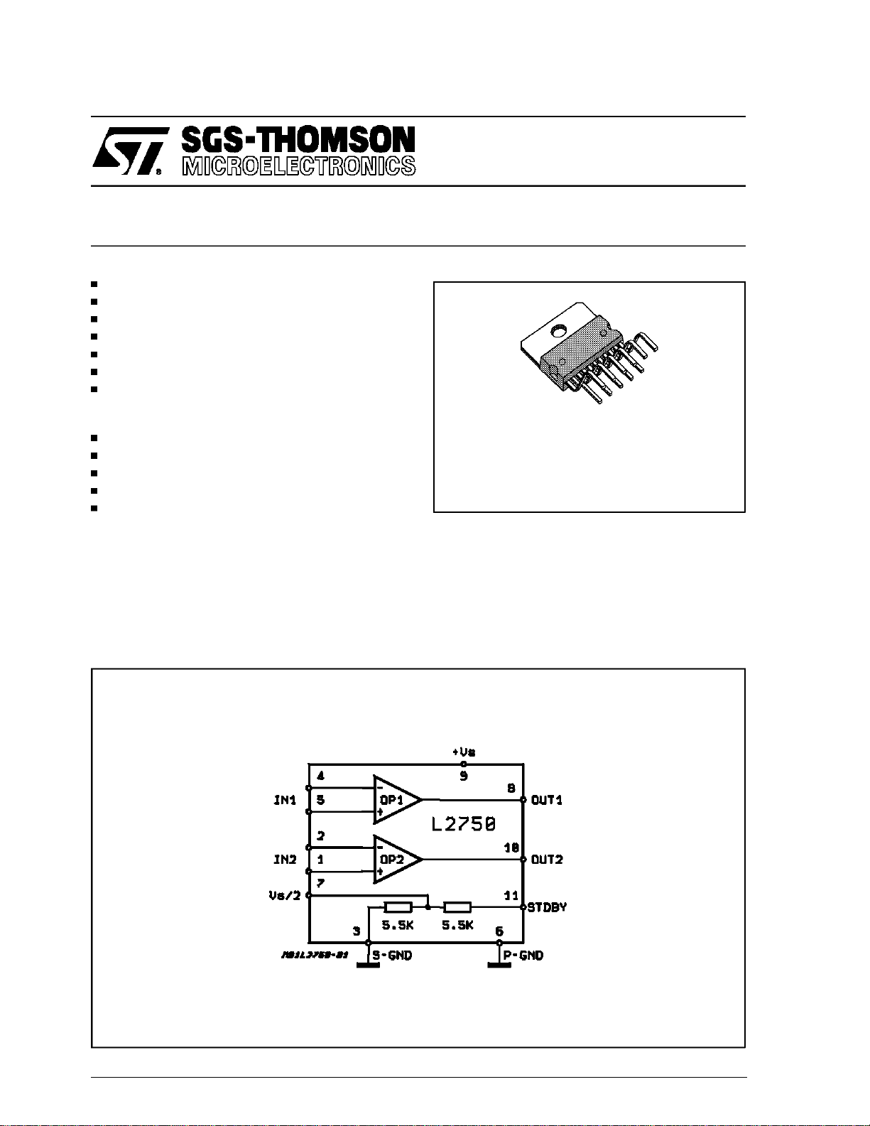
L2750
DUAL LOW DROP HIGH POWER
OPERATIONAL AMPLIFIER
ADVANCE DATA
PROTECTIONS:
VERYINDUCTIVE LOADS
OVERRATINGCHIP TEMPERATURE
LOADDUMP VOLTAGE
FORTUITOUS OPEN GROUND
ESD
DESCRIPTION
The L2750 is a new technology class AB dual
power operational amplifier assembled in Multiwatt 11 package.
Thanks to the fully complementaryPNP/NPN output configurationthe L2750 can deliver a rail-to-
BLOCK DIAGRAM
Multiwatt-11
ORDERING NUMBER: L2750
rail output voltage swing even at the highest current.
Additional feature is the very low current StandBy function.
Thehigh applicationflexibility of the L2750 makes
the device suitable for either motor driving/control
and audioapplicationspurposes.
October1991
This is advanced information on a new productnow in development or undergoing evaluation. Details are subject to change without notice.
1/10
L2750
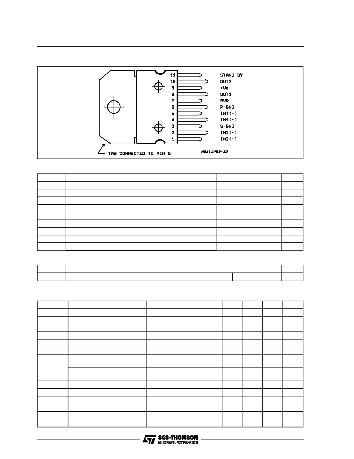
PIN CONNECTION (Top view)
ABSOLUTE MAXIMUMRATINGS
Symbol Parameter Value Unit
V
Sop
V
S max
V
PEAK
V
V
I
O
I
O
P
tot
T
stg,Tj
Operating Supply Voltage 18 V
Supply Voltage 28 V
Peak Supply Voltage (t = 50ms) 40 V
Input Voltage V
i
Differential Input Voltage V
i
Sop
Sop
Output Peak Current(non rep.t = 100µs) 5 A
Output Peak Current (rep. f > 10Hz) 4 A
Power Dissipation T
=85°C36W
CASE
Storage and JunctionTemperature -40 to 150 °C
V
V
THERMAL DATA
Symbol Description Value Unit
R
th j-case
Thermal Resistance Junction-case Max 1.8 °C/W
ELECTRICAL CHARACTERISTICS (Refer to the operational amplifier with GV= 24dB; VS= 14.4V;
T
=25°C,unless otherwisespecified
amb
Symbol Parameter Test Condition Min. Typ. Max. Unit
V
S
I
d
V
OS
I
SB
I
S
I
OS
V
DROP
SR Slew Rate 4 V/µs
B Gain Bandwidth Prod 10 MHz
G
V
R
IN
E
IN
CMRR Common Mode Rejection Ratio 75 90 dB
Supply Voltage 4 18 V
Total Quiescent Drain Current 30 50 mA
Input Offset Voltage 5 mV
ST-BY Current Consumption 50 µA
Input Bias Current 0.5 µA
Input Offset Current 50 nA
Output Voltage Drop (High) IO= 0.5A
I
=3A
O
Output Voltage Drop (Low) I
O
I
O
= 0.5A
=3A
0.25
1.1
0.25
1
0.5
2.5
0.5
2
V
V
V
V
Open Loop Voltage Gain f = 1KHz 85 dB
Input Resistance 150 MΩ
Input Noise Voltage Rs= 0 to10KΩ f = 22Hzto 22KHz 3 µV
2/10
ELECTRICALCHARACTERISTICS (continued)
Symbol Parameter Test Condition Min. Typ. Max. Unit
SVR Supply Voltage Rejection R
C
T
Crosstalk f = 1KHz to 10KHz 80 dB
=0
s
f = 100Hz
75 90 dB
L2750
APPLICATIONSUGGESTION
The high flexibilitymakes the L2750 suitable for a
wide range of applications.
Motor Controller
The device can be utilized as a motor controller.
Fig.1 represents a bidirectional DC motor control
suitablefor logic driving. In thesekinds of application it is possible to take advantage of the high
current capability of the L2750 for driving several
types of low impedance motors in a broad range
of applications.Moreover the low dropallows high
start up currents even at lowest supplyvoltage.
Audio Applications
Another typical utilization of the L2750 concerns
the audio field, as follows:
1) DRIVER FOR BOOSTER: The remarkably low
distortionand noise makesthedeviceproperto
be used as high quality driver for main amplifiers (i.e. car radio boosters). An example is
shownby Fig. 5, where thegainis setto 24 dB
(see alsothe relevantcharacteristics).
2) CAR RADIO BOOSTERWITH DIFFERENTIAL
INPUT : Fig. 10 shows an exampleof carradio
booster, with a gain of 30 dB, that is specially
recommendedfor active loudspeakers.Among
itsmain featureis the differentialinputand subsequent high noise suppression. The typical
output power delivered into a 4Ω load is 24W
=14.4V;d =10%),as shownby thecharac-
(V
S
teristicsenclosed.
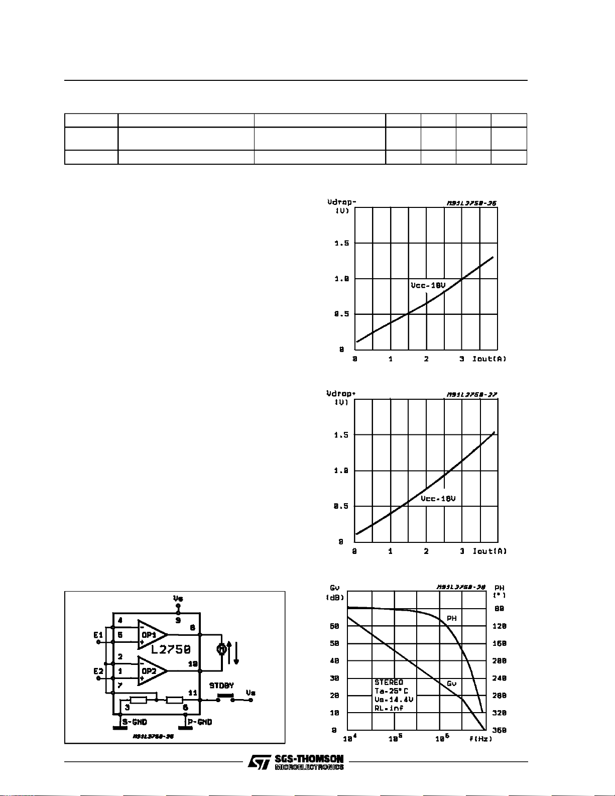
Figure2: Low Drop Voltage vs. Output Current
Figure3: High Drop Voltagevs. Output Current
Figure1
Figure4: Open Loop Gain vs. PhaseResponse
3/10

L2750
Figure5: Stereo Audio Amplifier ApplicationCircuit
Figure6: P.C. Board and ComponentsLayout of the Circuit of Figure 5 (1:1 scale)
4/10

AUDIO STEREOAPPLICATION CIRCUIT OF FIGURE 5
L2750
Figure7: QuiescentDrain Currentvs. Supply
Voltage
Figure9: Distortion vs. Frequency
Figure8: Distortionvs. Output Voltage
Figure10: Cross-Talkvs Frequency
Figure11:SupplyVoltageRejectionvs.Frequency
Figure12: E
Inputvs. R
N
g
5/10

L2750
Figure13: BridgePower Amplifier with BalancedInput Application Circuit
Figure14: P.C. Board and ComponentLayout of the Circuit ofFigure13 (1:1 scale)
6/10

BRIDGEAUDIO APPLICATION CIRCUIT OF FIGURE 13
L2750
Figure15: QuiescentDrain Current vs. Supply
Voltage
Figure17: OutputPower vs. Supply Voltage
Figure16: Noisevs. R
S
Figure18: OutputPower vs SupplyVoltage
Figure19: Distortionvs. OutputPower
Figure20: Distortionvs. Output Power
7/10

L2750
Figure21: Distortionvs. OutputPower
Figure23: Distortionvs. Frequency
Figure22: Distortionvs. Output Power
Figure24: SupplyVoltage Rejection vs. Fre-
quency
Figure25: TotalPower Dissipationand Effi-
ciencyvs. OutputPower
8/10
Figure26: TotalPower Dissipationand Effi-
ciencyvs. OutputPower

MULTIWATT11 PACKAGE MECHANICAL DATA
L2750
DIM.
A 5 0.197
B 2.65 0.104
C 1.6 0.063
D 1 0.039
E 0.49 0.55 0.019 0.022
F 0.88 0.95 0.035 0.037
G 1.57 1.7 1.83 0.062 0.067 0.072
G1 16.87 17 17.13 0.664 0.669 0.674
H1 19.6 0.772
H2 20.2 0.795
L 21.5 22.3 0.846 0.878
L1 21.4 22.2 0.843 0.874
L2 17.4 18.1 0.685 0.713
L3 17.25 17.5 17.75 0.679 0.689 0.699
L4 10.3 10.7 10.9 0.406 0.421 0.429
L7 2.65 2.9 0.104 0.114
M 4.1 4.3 4.5 0.161 0.169 0.177
M1 4.88 5.08 5.3 0.192 0.200 0.209
S 1.9 2.6 0.075 0.102
S1 1.9 2.6 0.075 0.102
Dia1 3.65 3.85 0.144 0.152
MIN. TYP. MAX. MIN. TYP. MAX.
mm inch
9/10

L2750
Information furnished is believed to be accurate and reliable. However, SGS-THOMSON Microelectronics assumes no responsibilityfor the
consequences of use of such information nor for any infringement ofpatents or otherrights of third parties which may result from its use. No
license is granted by implication or otherwise under any patent or patent rights of SGS-THOMSON Microelectronics. Specifications mentioned in thispublication are subject to change without notice. This publication supersedes and replaces all informationpreviously supplied.
SGS-THOMSON Microelectronics products are not authorized for use as critical components in lifesupport devices or systems without express writtenapproval of SGS-THOMSON Microelectronics.
1994 SGS-THOMSON Microelectronics - All RightsReserved
Australia - Brazil- France -Germany - Hong Kong - Italy - Japan- Korea - Malaysia - Malta - Morocco - The Netherlands- Singapore -
SGS-THOMSON Microelectronics GROUP OF COMPANIES
Spain - Sweden - Switzerland - Taiwan - Thaliand - United Kingdom - U.S.A.
10/10
 Loading...