


DUAL POWER OPERATIONAL AMPLIFIERS
.OUTPUTCURRENT TO1 A
.OPERATESAT LOW VOLTAGES
.SINGLEOR SPLITSUPPLY
.LARGE COMMON-MODE AND DIFFEREN-
TIALMODERANGE
.GROUNDCOMPATIBLEINPUTS
.LOWSATURATIONVOLTAGE
.THERMAL SHUTDOWN
DESCRIP TION
TheL272 isa monolithic integratedcircuits in Powerdip,Minidipand SO packagesintendedfor useas
poweroperationalamplifiers in a wide rangeof applicationsincludingservoamplifiersandpowersupplies,compacts disc, VCR, etc.
Thehighgainand high outputpower capabilityprovidesuperiorperformancewhateveranoperational
amplifier/powerboostercombinationisrequired.
L272
Powerdip
(8 +8)
Minidip
ORDERING NUMBERS : L272 (Powerdip)
SO16 (Narrow)
L272M (Minidip)
L272D (SO16 Narrow)
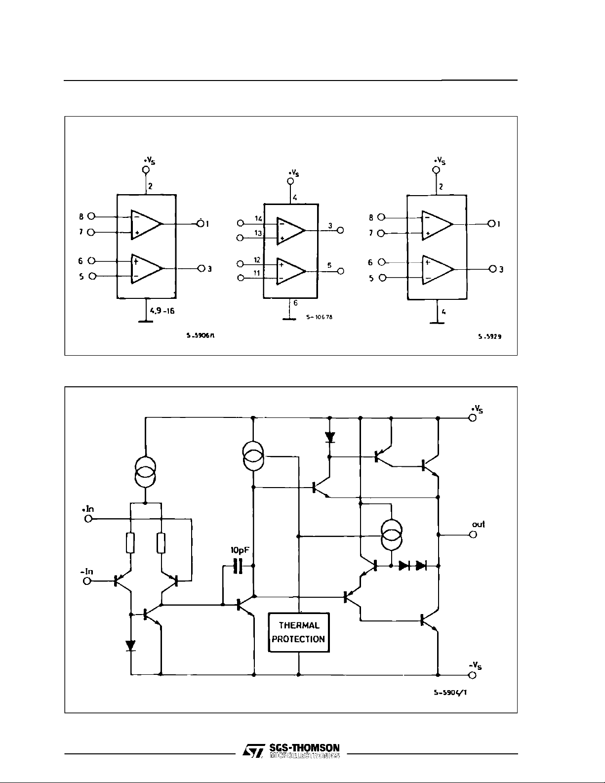
PIN CONNECTIONS (top view)
January 1995
L27 2M
L272D
1/10
L272
BLOCK DIAGRAMS
L272 L272ML272D
SCHEMATIC DIAGRAM (oneonly)
2/10
ABSOLUTE MAXIMUM RATINGS
Symbol Parameter Value Unit
V
V
V
I
o
I
p
P
tot
T
op
T
stg,Tj
s
Supply Voltage 28 V
Input Voltage V
i
Differential Input Voltage ± V
i
s
s
DC Output Current 1 A
Peak Output Current (non repetitive) 1.5 A
Power Dissipation at:
=80°C (L272), T
T
amb
=75°C (L272)
T
case
=50°C (L272M), T
amb
=90°C (L272D)
case
1.2
5
Operating Temperature Range (L272D) – 40 to 85 °C
Storage and Junction Temperature – 40 to 150 °C
THERMAL DATA
Symbol Parameter Powerdip SO16 Minidip Unit
R
th j-case
R
th j-amb
R
th j-alumina
* Thermal resistance junction-pin 4
** Thermal resistance junctions-pins with the chip soldered on the middle of an alumina supporting substrate measuring
15x 20mm; 0.65mm thickness and infinite heatsink.
Thermal Resistance Junction-pins Max. 15 – * 70
Thermal Resistance Junction-ambient Max. 70 – 100
Thermal Resistance Junction-alumina Max. – ** 50 –
L272
W
W
o
C/W
o
C/W
o
C/W
ELECTRICAL CHARACTERISTICS (VS= 24V, T
=25oC unless otherwise specified)
amb
Symbol Parameter Test Conditions Min. Typ. Max. Unit
V
s
I
s
I
b
V
os
I
os
Supply Voltage 4 28 V
Quiescent Drain Current VO=
S
V
= 24V
V
s
= 12V
s
2
8
7.51211mAmA
V
Input Bias Current 0.3 2.5 µA
Input Offset Voltage 15 60 mV
Input Offset Current 50 250 nA
SR Slew Rate 1V/µs
B Gain-bandwidth Product 350 kHz
R
G
v
e
N
I
N
Input Resistance 500 kΩ
i
O. L. Voltage Gain f = 100Hz
60 70
f = 1kHz
Input Noise Voltage B = 20kHz 10 µV
Input Noise Current B= 20kHz 200 pA
50
dB
dB
CRR Common Mode Rejection f = 1kHz 60 75 dB
SVR Supply Voltage Rejection f = 100Hz, R
= 24V
V
s
= ± 12V
V
s
= ± 6V
V
s
V
o
C
s
Output Voltage Swing Ip= 0.1A
= 0.5A 212322.5
I
p
Channel Separation f = 1 kHz; RL=10Ω,Gv= 30dB
= 24V
V
s
= ± 6V
V
s
d Distortion f = 1kHz, G
T
sd
Thermal Shutdown Junction
Temperature
= 10kΩ,VR= 0.5V
G
547062
56
60
60
= 3 dB, Vs= 24V, RL= ∞ 0.5 %
v
145 °C
dB
V
V
dB
3/10
 Loading...