

L2605
L2685-L2610
LOW DROPOUT VOLTAGE REGULATORS
OUTPUTVOLTAGE OF 5,8.5 AND 10 V
OUTPUTCURRENTUP TO 500 mA
NO EXTERNALCOMPONENTS
LOW DROPOUT VOLTAGE
OVERVOLTAGEPROTECTION (± 100V)
REVERSE VOLTAGEPROTECTION
SHORTCIRCUITPROTECTION
CURRENT LIMITING
THERMALSHUTDOWN
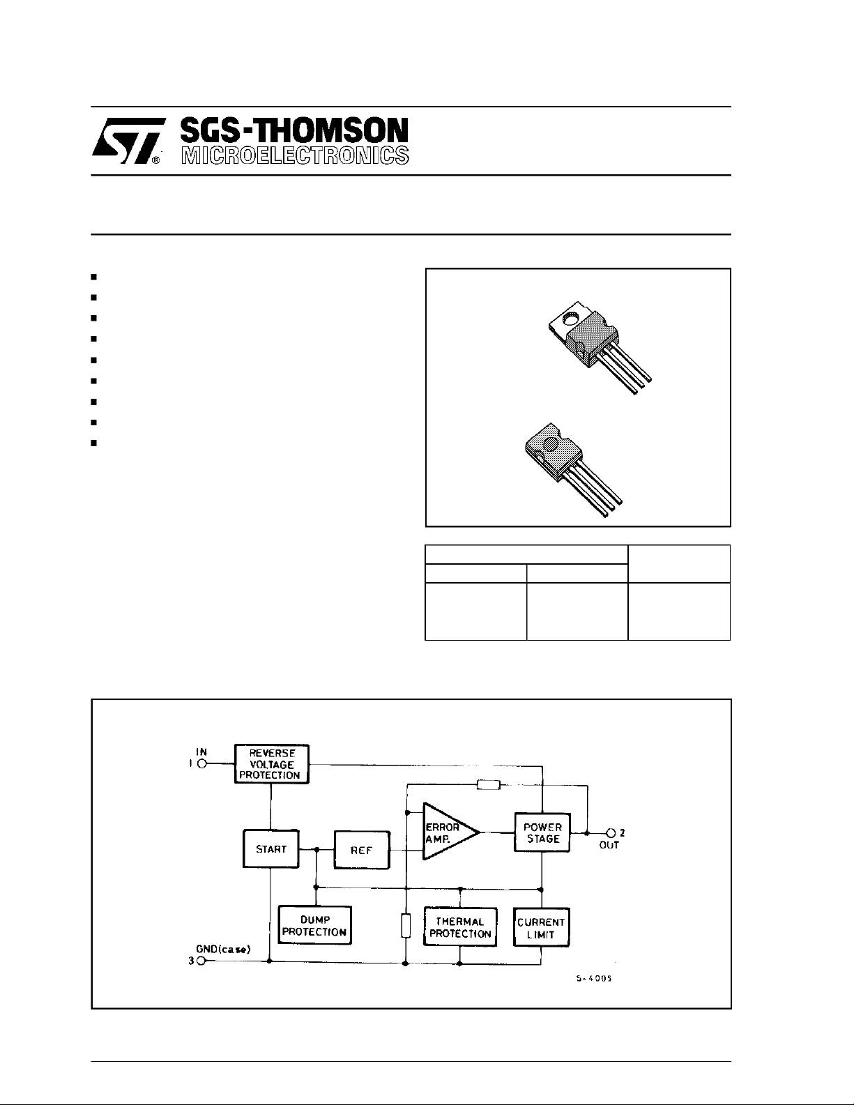
DESCRIPTION
The L2600 series og three terminal positive regulatorsis speciallydesigned to stabilizepower supplies car instrumentation in vehicles with 12V
battery. Availablewith outputvoltages equal to 5V,
8.5 V, 10V, they can supply an output current to
500mA.
These devices are protected against load dump
andfielddecay transients(±100V),reversebattery,
shortcircuit and thermal overload.
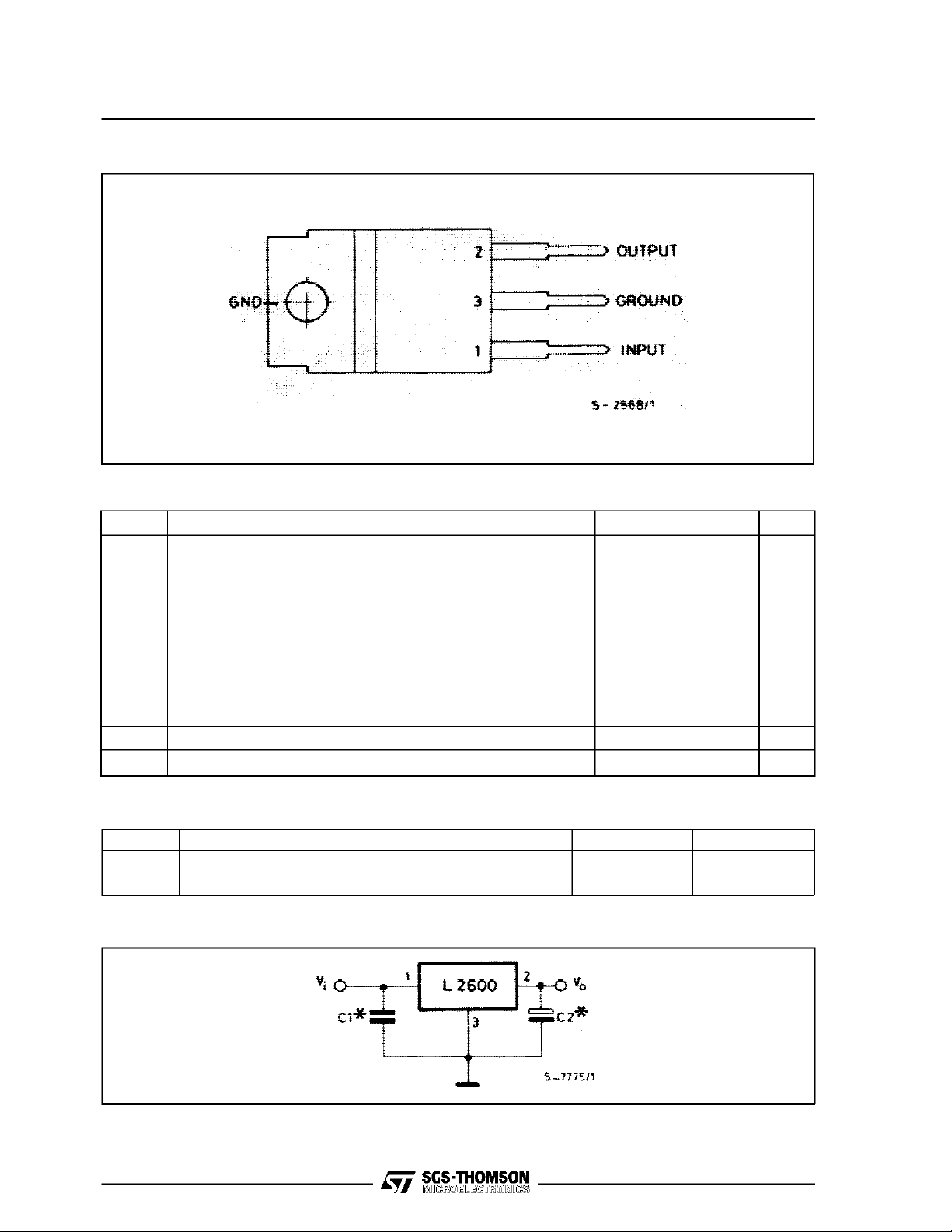
TO-220
SOT-82
Order codes
TO-220 SOT-82
L2605V L2605X 5 V
L2685V L2685X 8.5 V
L2610V L2610X 10 V
Output Voltage
BLOCKDIAGRAM
March 1993
1/6
L2605-L2685-L2610
PIN CONNECTION (top view)
ABSOLUTEMAXIMUM RATINGS
Symbol Parameter Value Unit
DC Input Voltage
V
P
Tj,T
i
DC Input Reverse Voltage
Transient Input Overvoltage:
Load Dump:
5ms ≤ t
Fall Time Costant = 100ms,
τ
f
R
source
≤ 10ms
rise
≥ 0.5 Ω
Field Decay:
5ms ≤ t
Rise Time Costant = 33ms,
τ
r
R
source
Power Dissipation Internally Limited
D
Junction and Storage Temperature Range - 55 to 150
stg
≤ 10ms
fall
≥ 10Ω
35
-28
+ 100
- 100
V
V
V
V
°C
THERMALDATA
Symbol Parameter SOT-82 TO-220
R
th-j-case
Rt
h-j-amb
Thermal resistance junction-case Max
Thermal resistance junction-ambient Max
8 °C/W 4°C/W
100 °C/W 75 ° C/W
APPLICATION CIRCUIT
(*) Note :C1andC2are only needed if the load capacitance exceeds 1000 pF, Recommended values are C1= 0.1 µF and
C2 ≥ 100 µF.
2/6

L2605-L2685-L2610
ELECTRICAL CHARACTERISTICS (Tj=25°C, Vi= 14V,unlessotherwise specified)
Symbol Parameter Test Condition Min. Typ. Max. Unit
V
V
∆ V
V
Output Voltage
o
Operating Input
i
= 500 mA
I
o
See Note (*) 28 V
Voltage
Line Regulation Io=50mA Vi= 12 to 20 V 2 8 mV/V
o
o
Load Regulation V
=14V Io= 50 to 500 mA 4 9 mV/V
i
V
= 12 to 16 V (L2605)
i
= 12 to 16 V (L2685)
V
i
V
= 12 to 16 V (L2610
i
4.80
8.15
9.60
5.00
8.50
10.00•
5.20
8.85
10.40
V
∆V
∆V
∆T
I
Dropout Voltage Io= 500 mA 1.9 V
i-o
I
Quiescent Current Io=50mA 20 45 mA
d
o
Output Voltage Drift I
Output Short Circuit
sc
=50mA
o
=14V
V
i
= - 12 to 80 °C
T
amb
-1 mV/°C
1.1 1.8 A
Current
SVR Supply Voltage
Rejection
R
e
Output Resistance Io= 500 mA 0.05 Ω
o
Output Noise Voltage BW = 100 Hz to 10 KHz 20 µ
N
=16
V
i
f = 100Hz
Vi=2V
I
= 500 mA 60 dB
o
V
(*) Note: For DC innput voltage 28 V <Vi<35 V the device is not operating
ELECTRICALCHARACTERISTICS (- 40≤ Tj≤ 125 °C(note 2), Vi= 14 V,unless otherwise specified)
Symbol Parameter TestCondition s Min. Typ. Max. Unit
V
o
V
i
Output Voltage
Operating Input
= 12.5 to 16 V (L2605)
V
I
= 500 mA
o
i
V
= 12.5 to 16 V (L2685)
i
= 12.5 to 16 V 2610)
V
i
See Note (°)26V
Voltage
4.70
8.00
9.40
5.00
8.50
10.00
5.30
9.00
10.60
V
∆V
V
∆V
I
LineRegulation Io=50mA Vi= 12.5 to 20 V 3 12 mV/V
o
o
LoadRegulation V
DropoutVoltage Io= 500 mA 2.5 V
i-o
I
Quiescent Current Io=50mA 29 65 mA
d
Output Short Circuit
sc
=14V Io= 50 to 500 mA, 5 13 mV/V
i
Current
Notes:(°). For a DC input voltage 26 V < Vi< 35 V the device is not operating.
2. The limits are guarandeed by designcorrelation and statistical control on production samples over the indicated
temperature and supply voltage ranges.
1.1 2.1 A
3/6

L2605-L2685-L2610
TO220PACKAGE MECHANICALDATA
DIM.
MIN. TYP. MAX. MIN. TYP. MAX.
A 4.8 0.189
C 1.37 0.054
D 2.4 2.8 0.094 0.110
D1 1.2 1.35 0.047 0.053
E 0.35 0.55 0.014 0.022
F 0.8 1.05 0.031 0.041
F2 1.15 1.4 0.045 0.055
G 4.95 5.08 5.21 0.195 0.200 0.205
H2 10.4 0.409
H3 10.05 10.4 0.396 0.409
L2 16.2 0.638
L3 26.3 26.7 27.1 1.035 1.051 1.067
L5 2.6 3 0.102 0.118
L6 15.1 15.8 0.594 0.622
L7 6 6.6 0.236 0.260
Dia 3.65 3.85 0.144 0.152
mm inch
4/6

SOT82 PACKAGE MECHANICAL DATA
L2605-L2685-L2610
DIM.
MIN. TYP. MAX. MIN. TYP. MAX.
A 7.4 7.8 0.291 0.307
B 10.5 10.8 0.413 0.425
b 0.7 0.9 0.028 0.035
b1 0.49 0.75 0.019 0.030
C 2.4 2.7 0.094 0.106
c1 1.2 0.047
D 15.7 0.618
e 2.2 0.087
e3 4.4 0.173
F 3.8 0.150
H 2.54 0.100
mm inch
5/6

L2605-L2685-L2610
Information furnished is believed to be accurate and reliable. However, SGS-THOMSON Microelectronics assumes no responsibility for the
consequences of use of such information nor for any infringement of patents or other rights of third parties which may result from its use. No
license is granted by implication or otherwise under any patent or patent rightsof SGS-THOMSON Microelectronics. Specifications mentioned
in this publication are subject to change without notice. This publication supersedes and replaces all information previously supplied.
SGS-THOMSON Microelectronics products are notauthorized foruse as critical components in life support devices or systems without express
written approval of SGS-THOMSON Microelectronics.
1994 SGS-THOMSON Microelectronics - All RightsReserved
SGS-THOMSON Microelectronics GROUP OF COMPANIES
Australia - Brazil - France - Germany - Hong Kong - Italy - Japan - Korea - Malaysia - Malta - Morocco - TheNetherlands - Singapore -
Spain - Sweden - Switzerland - Taiwan- Thaliand - United Kingdom - U.S.A.
6/6
 Loading...