


KF00
SERIES
VERY LOW DROP
VOLTAGE REGULATORS WITH INHIBIT
June 1998
■ VERYLOW DROPOUT VOLTAGE (0.4V)
■ VERYLOW QUIESCENTCURRENT
(TYP. 50µA IN OFF MODE, 500µAINON
MODE)
■ OUTPUTCURRENTUP TO 500mA
■ LOGIC-CONTROLLEDELECTRONIC
SHUTDOWN
■ OUTPUTVOLTAGESOF 1.25;1.5; 2.5; 2.7;
3; 3.3; 3.5; 4; 4.5; 4.7; 5; 5.2; 5.5; 6; 8; 8.5;
12V
■ INTERNALCURRENT ANDTHERMAL LIMIT
■ ONLY2.2µF FOR STABILITY
■ AVAILABLEIN ± 2%ACCURACY AT 25
o
C
■ SUPPLYVOLTAGEREJECTION:70 db
(TYP.)
■ TEMPERATURERANGE: -40 TO 125
o
C
DESCRIPTION
The KF00 series are very Low Drop regulators
availablein SO-8 package and in a widerange of
output voltages.
The very Low Drop voltage (0.4V) and the very
low quiescent current make them particularly
suitable for Low Noise, Low Power applications
and speciallyin batterypowered systems.
A Shutdown Logic Control function is available
(pin 5, TTL compatible). This means that when
the device is used as a local regulator, it is
possible to put a part of the board in standby,
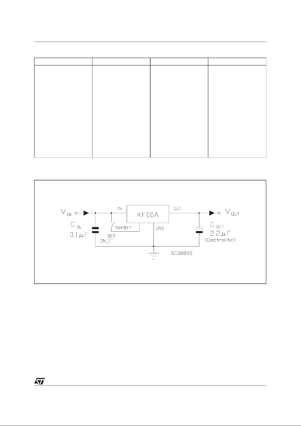
decreasing the total power consumption. It
requires only a 2.2 µF capacitor for stability
allowingspace and cost saving.
SCHEMATICDIAGRAM
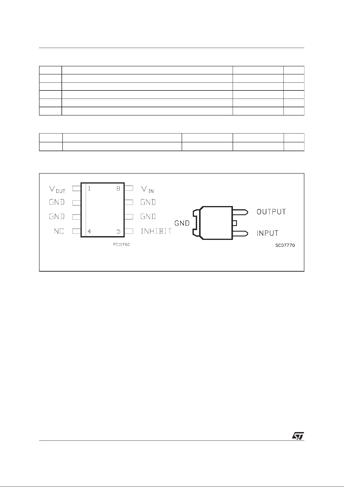
1
3
DPAKSO-8
1/16
ABSOLUTE MAXIMUMRATINGS
Symbol Parame t er Val u e Uni t
V
i
DC Input Voltage -0.5 to 20 V
I
o
Output Current Internally limited
P
tot
Power Dissipation Internally limited
T
stg
Storage Temperature Range - 40 to 150
o
C
T
op
Operating Junction Temperature Range - 40 to 125
o
C
CONNECTIONDIAGRAM (topview)
THERMAL DATA
Symbol Parame t er DPAK SO-8 Uni t
R
thj-case
Thermal Resistance Junction-case 8 20
o
C/W
DPAKSO-8
KF00
2/16
ORDERING NUMBERS
Typ e SO-8 DPAK Ou t put Volt ag e
KF12(*)
KF15(*)
KF25
KF27
KF30
KF33
KF35(*)
KF40
KF45(*)
KF47
KF50
KF52
KF55(*)
KF60
KF80
KF85
KF120
KF12BD
KF15BD
KF25BD
KF27BD
KF30BD
KF33BD
KF35BD
KF40BD
KF45BD
KF47BD
KF50BD
KF52BD
KF55BD
KF60BD
KF80BD
KF85BD
KF120BD
KF12BDT
KF15BDT
KF25BDT
KF27BDT
KF30BDT
KF33BDT
KF35BDT
KF40BDT
KF45BDT
KF47BDT
KF50BDT
KF52BDT
KF55BDT
KF60BDT
KF80BDT
KF85BDT
KF120BDT
1.25 V
1.5 V
2.5 V
2.7 V
3V
3.3 V
3.5 V
4V
4.5 V
4.75 V
5V
5.2 V
5.5 V
6V
8V
8.5V
12 V
(*) Available on request
TEST CIRCUITS
KF00
3/16

ELECTRICALCHARACTERISTICS FOR KF12 (refer to the test circuits, Tj=25oC,
C
i
=0.1 µF, Co= 2.2 µFunless otherwise specified)
Symbol Param et er Test Co ndi ti on s Min. Typ . Max. Unit
V
o
Output Voltage Io=50mA, Vi= 3.3 V
I
o
=50mA, Vi= 3.3 V -25<Ta<85oC
1.225
1.2
1.25 1.275
1.3
V
V
V
i
Operating Input Voltage Io= 500 mA 2.5 20 V
I
out
Output Current Limit 1 A
∆V
o
Line Regulation Vi= 2.5 to 20 V, Io=5mA 2 12 mV
∆V
o
Load Regulation Vi= 2.8 V Io= 5 to 500 mA 2 50 mV
I
d
Quiescent Current ON MODE
V
i
= 2.5 to 20 V Io=0mA
V
i
= 2.6 to 20 V Io= 500 mA
0.5 1
12
mA
mA
OFFMODE V
i
= 6 V 50 100 µA
SVR Supply Voltage Rejection
I
o
=5mA Vi= 3.5 V ± 1V
f = 120 Hz
f=1KHz
f = 10 KHz
82
77
60
dB
dB
dB
eN Output Noise Voltage B = 10 Hz to 100 KHz 50 µV
V
d
Dropout Voltage Io= 200 mA 1.25 V
V
il
Control Input Logic Low -40 < Ta<125oC0.8V
V
ih
Control Input Logic High -40 < Ta<125oC2 V
I
i
Control Input Current Vi=6V, Vc=6V 10 µA
C
O
Output Bypass Capacitance
ESR = 0.1 to 10 Ω I
o
=0to500mA
210 µF
ELECTRICALCHARACTERISTICS FOR KF15 (refer to the test circuits, Tj=25oC,
C
i
=0.1 µF, Co= 2.2 µFunless otherwise specified)
Symbol Param et er Test Co ndi ti on s Min. Typ . M a x. Un it
V
o
Output Voltage Io=50mA, Vi= 3.5 V
I
o
=50mA, Vi= 3.5 V -25<Ta<85oC
1.47
1.44
1.5 1.53
1.56
V
V
V
i
Operating Input Voltage Io= 500 mA 2.5 20 V
I
out
Output Current Limit 1 A
∆V
o
Line Regulation Vi= 2.5 to 20 V, Io=5mA 2 12 mV
∆V
o
Load Regulation Vi= 2.8 V Io= 5 to 500 mA 2 50 mV
I
d
Quiescent Current ON MODE
V
i
= 2.5 to 20 V Io=0mA
V
i
= 2.8 to 20 V Io= 500 mA
0.5 1
12
mA
mA
OFFMODE V
i
= 6 V 50 100 µA
SVR Supply Voltage Rejection
I
o
=5mA Vi= 3.5 V ± 1V
f = 120 Hz
f=1KHz
f = 10 KHz
82
77
60
dB
dB
dB
eN Output Noise Voltage B = 10 Hz to 100 KHz 50 µV
V
d
Dropout Voltage Io= 200 mA 1 V
V
il
Control Input Logic Low -40 < Ta<125oC0.8V
V
ih
Control Input Logic High -40 < Ta<125oC2 V
I
i
Control Input Current Vi=6V, Vc=6V 10 µA
C
O
Output Bypass Capacitance
ESR = 0.1 to 10 Ω I
o
=0to500mA
210 µF
KF00
4/16
ELECTRICALCHARACTERISTICS FOR KF25 (refer to the test circuits, Tj=25oC,
C
i
=0.1 µF, Co= 2.2 µFunless otherwise specified)
Symbol Param et er Test Co ndi ti on s Min. Typ . M a x. Un it
V
o
Output Voltage Io=50mA, Vi= 4.5 V
I
o
=50mA, Vi= 4.5 V -25<Ta<85oC
2.45
2.4
2.5 2.55
2.6
V
V
V
i
Operating Input Voltage Io= 500 mA 20 V
I
out
Output Current Limit 1 A
∆V
o
Line Regulation Vi= 3.5 to 20 V, Io=5mA 2 12 mV
∆V
o
Load Regulation Vi= 3.8 V Io= 5 to 500 mA 2 50 mV
I
d
Quiescent Current ON MODE
V
i
= 3.5 to 20 V Io=0mA
V
i
= 3.8 to 20 V Io= 500 mA
0.5 1
12
mA
mA
OFFMODE V
i
= 6 V 50 100 µA
SVR Supply Voltage Rejection
I
o
=5mA Vi= 4.5 V ± 1V
f = 120 Hz
f=1KHz
f = 10 KHz
82
77
60
dB
dB
dB
eN Output Noise Voltage B = 10 Hz to 100 KHz 50 µV
V
d
Dropout Voltage Io= 200 mA
I
o
= 500 mA
0.2
0.4
0.35
0.7
V
V
V
il
Control Input Logic Low -40 < Ta<125oC0.8V
V
ih
Control Input Logic High -40 < Ta<125oC2 V
I
i
Control Input Current Vi=6V, Vc=6V 10 µA
C
O
Output Bypass Capacitance
ESR = 0.1 to 10 Ω I
o
=0to500mA
210 µF
ELECTRICALCHARACTERISTICS FOR KF27 (refer to the test circuits, Tj=25oC,
C
i
=0.1 µF, Co= 2.2 µFunless otherwise specified)
Symbol Param et er Test Co ndi ti on s Min. Typ . M a x. Un it
V
o
Output Voltage Io=50mA, Vi= 4.7 V
I
o
=50mA, Vi= 4.7 V -25<Ta<85oC
2.646
2.592
2.7 2.754
2.808
V
V
V
i
Operating Input Voltage Io= 500 mA 20 V
I
out
Output Current Limit 1 A
∆V
o
Line Regulation Vi= 3.7 to 20 V, Io=5mA 2 12 mV
∆V
o
Load Regulation Vi=4V Io= 5 to 500 mA 2 50 mV
I
d
Quiescent Current ON MODE
V
i
= 3.7 to 20 V Io=0mA
V
i
= 4 to 20 V Io= 500 mA
0.5 1
12
mA
mA
OFFMODE V
i
= 6 V 50 100 µA
SVR Supply Voltage Rejection
I
o
=5mA Vi= 4.7 V ± 1V
f = 120 Hz
f=1KHz
f = 10 KHz
82
77
60
dB
dB
dB
eN Output Noise Voltage B = 10 Hz to 100 KHz 50 µV
V
d
Dropout Voltage Io= 200 mA
I
o
= 500 mA
0.2
0.4
0.35
0.7
V
V
V
il
Control Input Logic Low -40 < Ta<125oC0.8V
V
ih
Control Input Logic High -40 < Ta<125oC2 V
I
i
Control Input Current Vi=6V, Vc=6V 10 µA
C
O
Output Bypass Capacitance
ESR = 0.1 to 10 Ω I
o
=0to500mA
210 µF
KF00
5/16

ELECTRICALCHARACTERISTICS FOR KF30 (refer to the test circuits, Tj=25oC,
C
i
=0.1 µF, Co= 2.2 µFunless otherwise specified)
Symbol Param et er Test Co ndi ti on s Min. Typ . M a x. Un it
V
o
Output Voltage Io=50mA, Vi=5V
I
o
=50mA, Vi= 5 V -25<Ta<85oC
2.94
2.88
33.06
3.12
V
V
V
i
Operating Input Voltage Io= 500 mA 20 V
I
out
Output Current Limit 1 A
∆V
o
Line Regulation Vi= 4 to 20 V, Io= 5 mA 2 12 mV
∆V
o
Load Regulation Vi= 4.3 V Io= 5 to 500 mA 2 50 mV
I
d
Quiescent Current ON MODE
V
i
= 4 to 20 V Io=0mA
V
i
= 4.3 to 20 V Io= 500 mA
0.5 1
12
mA
mA
OFFMODE V
i
= 6 V 50 100 µA
SVR Supply Voltage Rejection
I
o
=5mA Vi=5V±1V
f = 120 Hz
f=1KHz
f = 10 KHz
81
76
60
dB
dB
dB
eN Output Noise Voltage B = 10 Hz to 100 KHz 50 µV
V
d
Dropout Voltage Io= 200 mA
I
o
= 500 mA
0.2
0.4
0.35
0.7
V
V
V
il
Control Input Logic Low -40 < Ta<125oC0.8V
V
ih
Control Input Logic High -40 < Ta<125oC2 V
I
i
Control Input Current Vi=6V, Vc=6V 10 µA
C
O
Output Bypass Capacitance
ESR = 0.1 to 10 Ω I
o
=0to500mA
210 µF
ELECTRICALCHARACTERISTICS FOR KF33 (refer to the test circuits, Tj=25oC,
C
i
=0.1 µF, Co= 2.2 µFunless otherwise specified)
Symbol Param et er Test Co ndi ti on s Min. Typ . M a x. Un it
V
o
Output Voltage Io=50mA, Vi= 5.3 V
I
o
=50mA, Vi= 5.3 V -25<Ta<85oC
3.234
3.168
3.3 3.366
3.432
V
V
V
i
Operating Input Voltage Io= 500 mA 20 V
I
out
Output Current Limit 1 A
∆V
o
Line Regulation Vi= 4.3 to 20 V, Io= 5 mA 2 12 mV
∆V
o
Load Regulation Vi= 4.6 V Io= 5 to 500 mA 2 50 mV
I
d
Quiescent Current ON MODE
V
i
= 4.3 to 20 V Io=0mA
V
i
= 4.6 to 20 V Io= 500 mA
0.5 1
12
mA
mA
OFFMODE V
i
= 6 V 50 100 µA
SVR Supply Voltage Rejection
I
o
=5mA Vi= 5.3 V ± 1V
f = 120 Hz
f=1KHz
f = 10 KHz
80
75
60
dB
dB
dB
eN Output Noise Voltage B = 10 Hz to 100 KHz 50 µV
V
d
Dropout Voltage Io= 200 mA
I
o
= 500 mA
0.2
0.4
0.35
0.7
V
V
V
il
Control Input Logic Low -40 < Ta<125oC0.8V
V
ih
Control Input Logic High -40 < Ta<125oC2 V
I
i
Control Input Current Vi=6V, Vc=6V 10 µA
C
O
Output Bypass Capacitance
ESR = 0.1 to 10 Ω I
o
=0to500mA
210 µF
KF00
6/16

ELECTRICALCHARACTERISTICS FOR KF35 (refer to the test circuits, Tj=25oC,
C
i
=0.1 µF, Co= 2.2 µFunless otherwise specified)
Symbol Param et er Test Co ndi ti on s Min. Typ . M a x. Un it
V
o
Output Voltage Io=50mA, Vi= 5.5 V
I
o
=50mA, Vi= 5.5 V -25<Ta<85oC
3.43
3.36
3.5 3.57
3.64
V
V
V
i
Operating Input Voltage Io= 500 mA 20 V
I
out
Output Current Limit 1 A
∆V
o
Line Regulation Vi= 4.5 to 20 V, Io=5mA 2 12 mV
∆V
o
Load Regulation Vi= 4.8 V Io= 5 to 500 mA 2 50 mV
I
d
Quiescent Current ON MODE
V
i
= 4.5 to 20 V Io=0mA
V
i
= 4.8 to 20 V Io= 500 mA
0.5 1
12
mA
mA
OFFMODE V
i
= 6 V 50 100 µA
SVR Supply Voltage Rejection
I
o
=5mA Vi= 5.5 V ± 1V
f = 120 Hz
f=1KHz
f = 10 KHz
79
74
60
dB
dB
dB
eN Output Noise Voltage B = 10 Hz to 100 KHz 50 µV
V
d
Dropout Voltage Io= 200 mA
I
o
= 500 mA
0.2
0.4
0.35
0.7
V
V
V
il
Control Input Logic Low -40 < Ta<125oC0.8V
V
ih
Control Input Logic High -40 < Ta<125oC2 V
I
i
Control Input Current Vi=6V, Vc=6V 10 µA
C
O
Output Bypass Capacitance
ESR = 0.1 to 10 Ω I
o
=0to500mA
210 µF
ELECTRICALCHARACTERISTICS FOR KF40 (refer to the test circuits, Tj=25oC,
C
i
=0.1 µF, Co= 2.2 µFunless otherwise specified)
Symbol Param et er Test Co ndi ti on s Min. Typ . M a x. Un it
V
o
Output Voltage Io=50mA, Vi=6V
I
o
=50mA, Vi= 6 V -25<Ta<85oC
3.92
3.84
44.08
4.16
V
V
V
i
Operating Input Voltage Io= 500 mA 20 V
I
out
Output Current Limit 1 A
∆V
o
Line Regulation Vi= 5 to 20 V, Io= 5 mA 3 18 mV
∆V
o
Load Regulation Vi= 5.3 V Io= 5 to 500 mA 2 50 mV
I
d
Quiescent Current ON MODE
V
i
= 5 to 20 V Io=0mA
V
i
= 5.3 to 20 V Io= 500 mA
0.5 1
12
mA
mA
OFFMODE V
i
= 6 V 50 100 µA
SVR Supply Voltage Rejection
I
o
=5mA Vi=6V±1V
f = 120 Hz
f=1KHz
f = 10 KHz
78
73
60
dB
dB
dB
eN Output Noise Voltage B = 10 Hz to 100 KHz 50 µV
V
d
Dropout Voltage Io= 200 mA
I
o
= 500 mA
0.2
0.4
0.35
0.7
V
V
V
il
Control Input Logic Low -40 < Ta<125oC0.8V
V
ih
Control Input Logic High -40 < Ta<125oC2 V
I
i
Control Input Current Vi=6V, Vc=6V 10 µA
C
O
Output Bypass Capacitance
ESR = 0.1 to 10 Ω I
o
=0to500mA
210 µF
KF00
7/16

ELECTRICALCHARACTERISTICS FOR KF45 (refer to the test circuits, Tj=25oC,
C
i
=0.1 µF, Co= 2.2 µFunless otherwise specified)
Symbol Param et er Test Co ndi ti on s Min. Typ . M a x. Un it
V
o
Output Voltage Io=50mA, Vi= 6.5 V
I
o
=50mA, Vi= 6.5 V -25<Ta<85oC
4.41
4.32
4.5 4.59
4.68
V
V
V
i
Operating Input Voltage Io= 500 mA 20 V
I
out
Output Current Limit 1 A
∆V
o
Line Regulation Vi= 5.5 to 20 V, Io=5mA 3 18 mV
∆V
o
Load Regulation Vi= 5.8 V Io= 5 to 500 mA 2 50 mV
I
d
Quiescent Current ON MODE
V
i
= 5.5 to 20 V Io=0mA
V
i
= 5.8 to 20 V Io= 500 mA
0.5 1
12
mA
mA
OFFMODE V
i
= 6 V 50 100 µA
SVR Supply Voltage Rejection
I
o
=5mA Vi= 6.5 V ± 1V
f = 120 Hz
f=1KHz
f = 10 KHz
77
72
60
dB
dB
dB
eN Output Noise Voltage B = 10 Hz to 100 KHz 50 µV
V
d
Dropout Voltage Io= 200 mA
I
o
= 500 mA
0.2
0.4
0.35
0.7
V
V
V
il
Control Input Logic Low -40 < Ta<125oC0.8V
V
ih
Control Input Logic High -40 < Ta<125oC2 V
I
i
Control Input Current Vi=6V, Vc=6V 10 µA
C
O
Output Bypass Capacitance
ESR = 0.1 to 10 Ω I
o
=0to500mA
210 µF
ELECTRICALCHARACTERISTICS FOR KF47 (refer to the test circuits, Tj=25oC,
C
i
=0.1 µF, Co= 2.2 µFunless otherwise specified)
Symbol Param et er Test Co ndi ti on s Min. Typ . M a x. Un it
V
o
Output Voltage Io=50mA, Vi= 6.7 V
I
o
=50mA, Vi= 6.7 V -25<Ta<85oC
4.606
4.512
4.7 4.794
4.888
V
V
V
i
Operating Input Voltage Io= 500 mA 20 V
I
out
Output Current Limit 1 A
∆V
o
Line Regulation Vi= 5.7 to 20 V, Io=5mA 3 18 mV
∆V
o
Load Regulation Vi=6V Io= 5 to 500 mA 2 50 mV
I
d
Quiescent Current ON MODE
V
i
= 5.7 to 20 V Io=0mA
V
i
= 6 to 20 V Io= 500 mA
0.5 1
12
mA
mA
OFFMODE V
i
= 6 V 50 100 µA
SVR Supply Voltage Rejection
I
o
=5mA Vi= 6.7 V ± 1V
f = 120 Hz
f=1KHz
f = 10 KHz
77
72
60
dB
dB
dB
eN Output Noise Voltage B = 10 Hz to 100 KHz 50 µV
V
d
Dropout Voltage Io= 200 mA
I
o
= 500 mA
0.2
0.4
0.35
0.7
V
V
V
il
Control Input Logic Low -40 < Ta<125oC0.8V
V
ih
Control Input Logic High -40 < Ta<125oC2 V
I
i
Control Input Current Vi=6V, Vc=6V 10 µA
C
O
Output Bypass Capacitance
ESR = 0.1 to 10 Ω I
o
=0to500mA
210 µF
KF00
8/16

ELECTRICALCHARACTERISTICS FOR KF50 (refer to the test circuits, Tj=25oC,
C
i
=0.1 µF, Co= 2.2 µFunless otherwise specified)
Symbol Param et er Test Co ndi ti on s Min. Typ . M a x. Un it
V
o
Output Voltage Io=50mA, Vi=7V
I
o
=50mA, Vi= 7 V -25<Ta<85oC
4.9
4.8
55.1
5.2
V
V
V
i
Operating Input Voltage Io= 500 mA 20 V
I
out
Output Current Limit 1 A
∆V
o
Line Regulation Vi= 6 to 20 V, Io=5mA 3 18 mV
∆V
o
Load Regulation Vi= 6.3 V Io= 5 to 500 mA 2 50 mV
I
d
Quiescent Current ON MODE
V
i
= 6 to 20 V Io=0mA
V
i
= 6.3 to 20 V Io= 500 mA
0.5 1
12
mA
mA
OFFMODE V
i
= 6 V 50 100 µA
SVR Supply Voltage Rejection
I
o
=5mA Vi=7 V ± 1V
f = 120 Hz
f=1KHz
f = 10 KHz
76
71
60
dB
dB
dB
eN Output Noise Voltage B = 10 Hz to 100 KHz 50 µV
V
d
Dropout Voltage Io= 200 mA
I
o
= 500 mA
0.2
0.4
0.35
0.7
V
V
V
il
Control Input Logic Low -40 < Ta<125oC0.8V
V
ih
Control Input Logic High -40 < Ta<125oC2 V
I
i
Control Input Current Vi=6V, Vc=6V 10 µA
C
O
Output Bypass Capacitance
ESR = 0.1 to 10 Ω I
o
=0to500mA
210 µF
ELECTRICALCHARACTERISTICS FOR KF52 (refer to the test circuits, Tj=25oC,
C
i
=0.1 µF, Co= 2.2 µFunless otherwise specified)
Symbol Param et er Test Co ndi ti on s Min. Typ . M a x. Un it
V
o
Output Voltage Io=50mA, Vi= 7.2 V
I
o
=50mA, Vi= 7.2 V -25<Ta<85oC
5.096
4.992
5.2 5.304
5.408
V
V
V
i
Operating Input Voltage Io= 500 mA 20 V
I
out
Output Current Limit 1 A
∆V
o
Line Regulation Vi= 6.2 to 20 V, Io= 5 mA 3 18 mV
∆V
o
Load Regulation Vi= 6.5 V Io= 5 to 500 mA 2 50 mV
I
d
Quiescent Current ON MODE
V
i
= 6.2 to 20 V Io=0mA
V
i
= 6.5 to 20 V Io= 500 mA
0.5 1
12
mA
mA
OFFMODE V
i
= 6 V 50 100 µA
SVR Supply Voltage Rejection
I
o
=5mA Vi= 7.2 V ± 1V
f = 120 Hz
f=1KHz
f = 10 KHz
76
71
60
dB
dB
dB
eN Output Noise Voltage B = 10 Hz to 100 KHz 50 µV
V
d
Dropout Voltage Io= 200 mA
I
o
= 500 mA
0.2
0.4
0.35
0.7
V
V
V
il
Control Input Logic Low -40 < Ta<125oC0.8V
V
ih
Control Input Logic High -40 < Ta<125oC2 V
I
i
Control Input Current Vi=6V, Vc=6V 10 µA
C
O
Output Bypass Capacitance
ESR = 0.1 to 10 Ω I
o
=0to500mA
210 µF
KF00
9/16

ELECTRICALCHARACTERISTICS FOR KF55 (refer to the test circuits, Tj=25oC,
C
i
=0.1 µF, Co= 2.2 µFunless otherwise specified)
Symbol Param et er Test Co ndi ti on s Min. Typ . M a x. Un it
V
o
Output Voltage Io=50mA, Vi= 7.5 V
I
o
=50mA, Vi= 7.5 V -25<Ta<85oC
5.39
5.28
5.5 5.61
5.72
V
V
V
i
Operating Input Voltage Io= 500 mA 20 V
I
out
Output Current Limit 1 A
∆V
o
Line Regulation Vi= 6.5 to 20 V, Io= 5 mA 3 18 mV
∆V
o
Load Regulation Vi= 6.8 V Io= 5 to 500 mA 2 50 mV
I
d
Quiescent Current ON MODE
V
i
= 6.5 to 20 V Io=0mA
V
i
= 6.8 to 20 V Io= 500 mA
0.5 1
12
mA
mA
OFFMODE V
i
= 6 V 50 100 µA
SVR Supply Voltage Rejection
I
o
=5mA Vi=7.5 V ± 1V
f = 120 Hz
f=1KHz
f = 10 KHz
76
71
60
dB
dB
dB
eN Output Noise Voltage B = 10 Hz to 100 KHz 50 µV
V
d
Dropout Voltage Io= 200 mA
I
o
= 500 mA
0.2
0.4
0.35
0.7
V
V
V
il
Control Input Logic Low -40 < Ta<125oC0.8V
V
ih
Control Input Logic High -40 < Ta<125oC2 V
I
i
Control Input Current Vi=6V, Vc=6V 10 µA
C
O
Output Bypass Capacitance
ESR = 0.1 to 10 Ω I
o
=0to500mA
210 µF
ELECTRICALCHARACTERISTICS FOR KF60 (refer to the test circuits, Tj=25oC,
C
i
=0.1 µF, Co= 2.2 µFunless otherwise specified)
Symbol Param et er Test Co ndi ti on s Min. Typ . M a x. Un it
V
o
Output Voltage Io=50mA, Vi=8V
I
o
=50mA, Vi= 8 V -25<Ta<85oC
5.88
5.76
66.12
6.24
V
V
V
i
Operating Input Voltage Io= 500 mA 20 V
I
out
Output Current Limit 1 A
∆V
o
Line Regulation Vi= 7 to 20 V, Io=5mA 4 24 mV
∆V
o
Load Regulation Vi= 7.3 V Io= 5 to 500 mA 2 50 mV
I
d
Quiescent Current ON MODE
V
i
= 7 to 20 V Io=0mA
V
i
= 7.3 to 20 V Io= 500 mA
0.7 1. 5
12
mA
mA
OFFMODE V
i
= 9 V 70 140 µA
SVR Supply Voltage Rejection
I
o
=5mA Vi=8V±1V
f = 120 Hz
f=1KHz
f = 10 KHz
75
70
60
dB
dB
dB
eN Output Noise Voltage B = 10 Hz to 100 KHz 50 µV
V
d
Dropout Voltage Io= 200 mA
I
o
= 500 mA
0.2
0.4
0.35
0.7
V
V
V
il
Control Input Logic Low -40 < Ta<125oC0.8V
V
ih
Control Input Logic High -40 < Ta<125oC2 V
I
i
Control Input Current Vi=9V, Vc=6V 10 µA
C
O
Output Bypass Capacitance
ESR = 0.1 to 10 Ω I
o
=0to500mA
210 µF
KF00
10/16

ELECTRICALCHARACTERISTICS FOR KF80B (refer to the test circuits, Tj=25oC,
C
i
=0.1 µF, Co= 2.2 µFunless otherwise specified)
Symbol Param et er Test Co ndi ti on s Min. Typ . M a x. Un it
V
o
Output Voltage Io=50mA, Vi=10V
I
o
=50mA, Vi= 10 V -25<Ta<85oC
7.84
7.68
88.16
8.32
V
V
V
i
Operating Input Voltage Io= 500 mA 20 V
I
out
Output Current Limit 1 A
∆V
o
Line Regulation Vi= 9 to 20 V, Io=5mA 4 24 mV
∆V
o
Load Regulation Vi= 9.3 V Io= 5 to 500 mA 2 50 mV
I
d
Quiescent Current ON MODE
V
i
= 9 to 20 V Io=0mA
V
i
= 9.3 to 20 V Io= 500 mA
0.7 1. 5
12
mA
mA
OFFMODE V
i
= 9 V 70 140 µA
SVR Supply Voltage Rejection
I
o
=5mA Vi=10 V ± 1V
f = 120 Hz
f=1KHz
f = 10 KHz
72
67
60
dB
dB
dB
eN Output Noise Voltage B = 10 Hz to 100 KHz 50 µV
V
d
Dropout Voltage Io= 200 mA
I
o
= 500 mA
0.2
0.4
0.35
0.7
V
V
V
il
Control Input Logic Low -40 < Ta<125oC0.8V
V
ih
Control Input Logic High -40 < Ta<125oC2 V
I
i
Control Input Current Vi=9V, Vc=6V 10 µA
C
O
Output Bypass Capacitance
ESR = 0.1 to 10 Ω I
o
=0to500mA
210 µF
ELECTRICALCHARACTERISTICS FOR KF85B (refer to the test circuits, Tj=25oC,
C
i
=0.1 µF, Co= 2.2 µFunless otherwise specified)
Symbol Param et er Test Co ndi ti on s Min. Typ . M a x. Un it
V
o
Output Voltage Io=50mA,Vi= 10.5V
I
o
=50mA,Vi= 10.5V -25<Ta<85oC
8.33
8.16
8.5 8.67
8.84
V
V
V
i
Operating Input Voltage Io= 500 mA 20 V
I
out
Output Current Limit 1 A
∆V
o
Line Regulation Vi= 9.5 to 20 V, Io= 5 mA 4 24 mV
∆V
o
Load Regulation Vi= 9.8 V Io= 5 to 500 mA 2 50 mV
I
d
Quiescent Current ON MODE
V
i
= 9.5 to 20 V Io=0mA
V
i
= 9.8 to 20 V Io= 500 mA
0.7 1. 5
12
mA
mA
OFFMODE V
i
= 10 V 70 140 µA
SVR Supply Voltage Rejection
I
o
=5mA Vi= 10.5 V ± 1V
f = 120 Hz
f=1KHz
f = 10 KHz
67
63
53
dB
dB
dB
eN Output Noise Voltage B = 10 Hz to 100 KHz 50 µV
V
d
Dropout Voltage Io= 200 mA
I
o
= 500 mA
0.2
0.4
0.35
0.7
V
V
V
il
Control Input Logic Low -40 < Ta<125oC0.8V
V
ih
Control Input Logic High -40 < Ta<125oC2 V
I
i
Control Input Current Vi=10V, Vc=6V 10 µA
C
O
Output Bypass Capacitance
ESR = 0.1 to 10 Ω I
o
=0to500mA
210 µF
KF00
11/16

ELECTRICALCHARACTERISTICS FOR KF120B (refer to the test circuits,Tj=25oC,
C
i
=0.1 µF, Co= 2.2 µFunless otherwise specified)
Symbol Param et er Test Co ndi ti on s Min. Typ . M a x. Un it
V
o
Output Voltage Io=50mA, Vi=14V
I
o
=50mA, Vi= 14 V -25<Ta<85oC
11.76
11.52
12 12.24
12.48
V
V
V
i
Operating Input Voltage Io= 500 mA 20 V
I
out
Output Current Limit 1 A
∆V
o
Line Regulation Vi=13to20V, Io= 5 mA 8 48 mV
∆V
o
Load Regulation Vi= 13.3 V Io=5to500mA 2 50 mV
I
d
Quiescent Current ON MODE
V
i
=13to20V Io=0mA
V
i
= 13.3 to 20 V Io= 500 mA
0.7 1. 5
12
mA
mA
OFFMODE V
i
= 13 V 70 140 µA
SVR Supply Voltage Rejection
I
o
=5mA Vi=14V±1V
f = 120 Hz
f=1KHz
f = 10 KHz
69
64
54
dB
dB
dB
eN Output Noise Voltage B = 10 Hz to 100 KHz 50 µV
V
d
Dropout Voltage Io= 200 mA
I
o
= 500 mA
0.2
0.4
0.35
0.7
V
V
V
il
Control Input Logic Low -40 < Ta<125oC0.8V
V
ih
Control Input Logic High -40 < Ta<125oC2 V
I
i
Control Input Current Vi=13V, Vc=6V 10 µA
C
O
Output Bypass Capacitance
ESR = 0.1 to 10 Ω I
o
=0to500mA
210 µF
KF00
12/16

DropoutVoltagevs Output Current
Supply Currentvs Input Voltage
Short Circuit Currentvs Input Voltage
SupplyCurrentvs Input Voltage
SupplyVoltage Rejection vs Input Voltage
TYPICALPERFORMANCE CHARACTERISTICS (unlessotherwisespecifiedV
o(NOM)
=3.3V)
DropoutVoltage vs Temperature
KF00
13/16

DIM.
mm inch
MIN. TYP. MAX. MIN. TYP. MAX.
A 1.75 0.068
a1 0.1 0.25 0.003 0.009
a2 1.65 0.064
a3 0.65 0.85 0.025 0.033
b 0.35 0.48 0.013 0.018
b1 0.19 0.25 0.007 0.010
C 0.25 0.5 0.010 0.019
c1 45 (typ.)
D 4.8 5.0 0.188 0.196
E 5.8 6.2 0.228 0.244
e 1.27 0.050
e3 3.81 0.150
F 3.8 4.0 0.14 0.157
L 0.4 1.27 0.015 0.050
M 0.6 0.023
S 8 (max.)
0016023
SO-8 MECHANICALDATA
KF00
14/16

DIM.
mm inch
MIN. TYP. MAX. MIN. TYP. MAX.
A 2.2 2.4 0.086 0.094
A1 0.9 1.1 0.035 0.043
A2 0.03 0.23 0.001 0.009
B 0.64 0.9 0.025 0.035
B2 5.2 5.4 0.204 0.212
C 0.45 0.6 0.017 0.023
C2 0.48 0.6 0.019 0.023
D 6 6.2 0.236 0.244
E 6.4 6.6 0.252 0.260
G 4.4 4.6 0.173 0.181
H 9.35 10.1 0.368 0.397
L2 0.8 0.031
L4 0.6 1 0.023 0.039
==
D
L2
L4
13
==
B
E
==
B2
G
2
A
C2
C
H
A1
DETAIL”A”
A2
DETAIL”A”
TO-252 (DPAK) MECHANICAL DATA
0068772-B
KF00
15/16

Information furnished is believed tobe accurate and reliable. However, STMicroelectronics assumes no responsibility for theconsequences
of use of such information nor for any infringement of patents or other rights of third parties which may result from its use. No license is
granted by implication or otherwise under any patent or patent rights of STMicroelectronics. Specification mentioned in this publication are
subject to change without notice. This publication supersedes and replaces all information previously supplied. STMicroelectronics products
are not authorized for use as critical components in life support devices or systems without express written approval of STMicroelectronics.
The ST logo is a trademark of STMicroelectronics
1998 STMicroelectronics – Printed in Italy – All Rights Reserved
STMicroelectronicsGROUP OF COMPANIES
Australia - Brazil -Canada - China - France - Germany - Italy - Japan -Korea - Malaysia - Malta - Morocco - The Netherlands -
Singapore - Spain - Sweden - Switzerland - Taiwan - Thailand - UnitedKingdom - U.S.A.
.
KF00
16/16
 Loading...