

SGS Thomson Microelectronics HCF4056B, HCF4055B, HCF4054B Datasheet
LIQUID-CRYSTAL DISPLAY DRIVERS
4054B 4-SEGMENT DISPLAY DRIVER -
STROB ED LATCH FUNCTION
4055B B CD TO 7-SEGMENT
DECODER/DRIVER, WITH ”DISPLAY-FREQUENCY” OUTPUT
4056B B CD TO 7-SEGMENT
DECODER/DRIVER WITH
STROB ED LATCH FUNCTION
.QUIESCENT CURRENT SPECIFIED TO 20V
FOR HCC DEVICE
.OPERATION OF LIQUID CRYSTALS WITH
COS/MOS CIRCUITS PROVIDES ULTRALOW-POWER DISPLAYS
.EQUIVALENT AC OUTPUT DRIVE FOR LI-
QUID-CRYSTAL DISPLAYS-NO EXTERNAL
CAPACITOR REQUIRED
.VOLTAGE DOUBLING ACROSS DISPLAY
[(VDD–VEE) = 18V)] RESULTS IN EFFECTIVE
36V (p-p) DRIVE ACROSS SELECTED DISPLAY SEGMENTS
.LOW-OR HIGH-OUTPUT LEVEL DC DRIVE
FOR OTHER TYPES OF DISPLAYS
.ON-CHIP LOGIC-LEVEL CONVERSION FOR
DIFFERENT INPUT AND OUTPUT-LEVEL
SWINGS
.FULL DECODING OF ALL INPUT COMBINA-
TIONS: ”0 – 9, L, H, P, A– ” AND BLANK POSITIONS
.INPUT CURRENTOF100nAAT 18V AND 25°C
FOR HCC DEVICE
.100% TESTEDFOR QUIESCENTCURRENT
.MEETSALLREQUIREMENTSOFJEDECTEN-
TATIVE STANDARD N°. 13A, ”STANDARD
SPECIFICATIONS FOR DESCRIPTION OF ”B”
SERIESCMOS DEVICES”
DESCRIPTION
The HCC4054B, HCC4055B and HCC4056B (ex-
tended temperature range) and the HCF4054B,
HCF4055B and HCF4056B (intermediate temperaturerange) aremonolithicintegratedcircuitsavailable
in 16-lead dual in-line plastic orceramic package and
plastic micro package. The HCC/HCF4055B and
HCC/HCF4056B typesare single-digit BCD-to-7-segment decoder/driver circuits that provide level-shifting
functions on the chip. This feature permits the BCD
input-signal swings (VDDtoVSS) to be thesame as
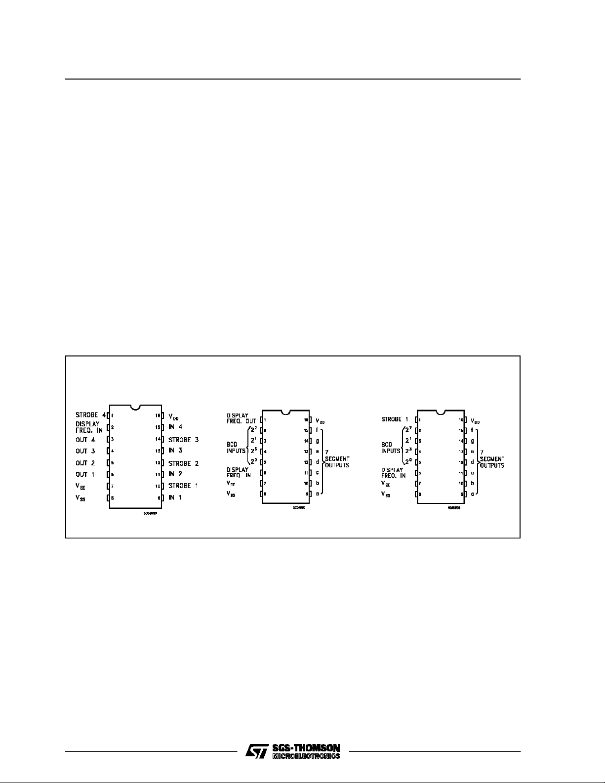
HCC4054B/55B/56B
HCF4054B/55B/56B
EY
(Plastic Package)F(Ceramic Frit SealPackage)
M1
(MicroPackage)
ORDER CODES :
HCC40XXBF HCF40XXBM1
HCF40XXBEY HCF40XXBC1
ordifferentfromthe7-segmentoutput-signalswings
(VDDto VEE). For example, the BCD input-signal
swings (VDDto VSS) may be as low as 0 to – 3V,
whereasthe output-display drive-signal swing (V
to VEE)maybefrom0to–5V.IfVDDtoVEEexceeds
15V, VDDto VSSshould be at least 4V. The 7-segment outputs are controlled by the DISPLAY-FREQUENCY (DF) input which causes the selected
segmentoutputs to below, high, or a square-wave
output (for liquid-crystal displays). When the DF
input is low the output segments will be high when
selected by the BCD inputs. When the DF input is
high,theoutputsegments will belowwhenselected
by the BCD inputs. When a square-wave ispresent
at the DF input, the selected segments will have a
square-wave output thatis 180° out of phase with
the DF input. Those segments which are not selected will have a square-wave output that is in
phase with the input. DF square-wave repetition
rates for liquid-crystal displays usually range from
30Hz (well above flicker rate) to 200Hz (well below
the upper limit of the liquid-crystal frequency response). The HCC/HCF4055B provides a levelshifted high-amplitude DF output which is required
for driving the common electrode in liquid-crystal
displays. The HCC/HCF4056B provides a strobedlatch function at the BCD inputs. Decoding of all
input combinations on the HCC/HCF4055B and
HCC/HCF4056Bprovides displays of 0 to 9as well
(PlasticChipCarrier)
C1
DD
March 1989
1/15
HCC/H CF4054B/55B/56B
as L, P, H, A,–, andablank position.(see typical application for other letters). The HCC/HCF4054B pro-
vides level shifting similar to the HCC/HCF4055B
andHCC/HCF4056B independently strobedlatches,
and common DF control on 4 signal lines. The
HCC/HCF4054Bisintended toprovide drive-signal
compatibility with the HCC/HCF4055B and
HCC/HCF4056B 7-segment decoder types for the
decimalpoint,colon,polarity,andsimilardisplaylines.
A level-shifted high-amplitude DF output canbe obtainedfrom anyHCC/HCF4054B outputlinebycon-
necting the corresponding inputand strobe lines to
a low and high level, respectively. The
HCC/HCF4054Bmayalso be utilizedfor logic-level
”upconversion” or ”downconversion”. Forexample,
input-signal swings (VDDtoVSS) from + 5 to 0V can
be convertedtooutput-signal swings(VDDtoVEE)of
+ 5 to – 5V. The level-shifted function on all three
types permits the use of different input-and outputsignal swings. The inputswingsfrom a lowlevelof
VSSto a high level of VDDwhile the output swings
PIN CONNECTIONS
4054B 4055B 4056B
fromalowlevel ofVEEtothesame highlevel ofVDD.
Thus, the inputand output swings can be selected
independently of each otherovera 3-to-18V range.
VSSmay be connected to VEEwhen no level-shift
function is required. For the HCC/HCF 4054B and
HCC/HCF4056B, dataaretransferredfrominput to
output by placing a high voltage level at thestrobe
input. A low voltage levelat the strobe input latches
the data input and the corresponding output segments remain selected (or non-selected) whilethe
strobe is low.Whenever the level-shifting function
is required, the HCC/HCF4055B can be usedby it-
self to drive a liquid-crystal display (fig. 10 and fig.
12). The HCC/HCF4056B, however,must be used
together withaHCC/HCF4054Btoprovide thecommon DFoutput (fig. 14).Thecapability of extending
the voltage swing on thenegative end(this voltage
cannot be extended on the positive end) can be
used to advantage in theset-up of fig.11. Fig. 9 is
commonto all three types.
2/15
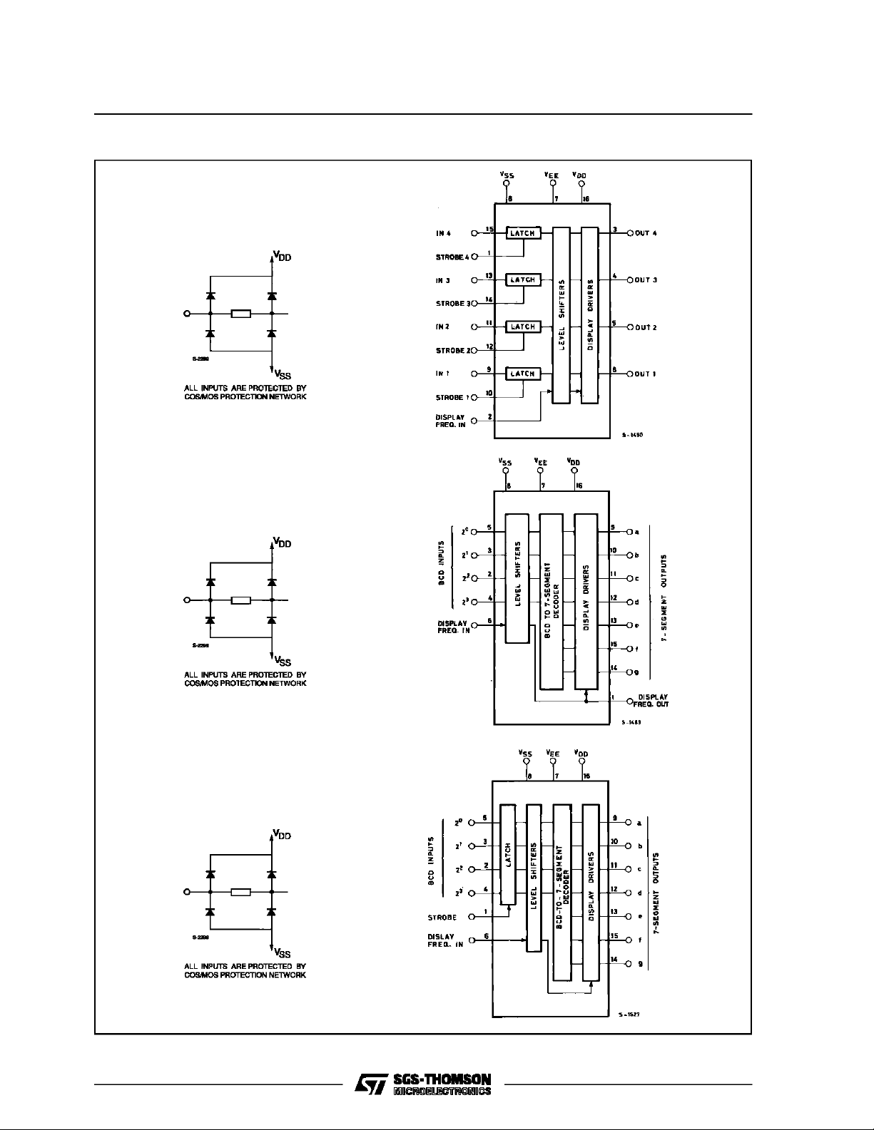
FUNCTIONAL DIAGRAMS
4054B
4055B
HCC/HCF4054B/55B/56B
4056B
3/15
HCC/H CF4054B/55B/56B
ABSOLUTE MAXIMUM RAT IN G S
Symbol Parameter Value Unit
V
* Supply Voltage :HCC Types
DD
V
Input Voltage – 0.5 to VDD+ 0.5 V
i
I
DC Input Current (any one input) ± 10 mA
I
P
T
T
Stresses above those listed under ”Absolute Maximum Ratings” may cause permanent damage to the device. This is a stress rating only
and functional operation of the device at these or any other conditions above those indicated in the operational sections of this specification
is not implied. Exposure to absolute maximum rating conditions for external periods may affect device reliability.
* Allvoltage valuesarereferred to VSSpinvoltage.
Total Power Dissipation (per package)
tot
Dissipation per Output Transistor
for Top= Full Package-temperature Range
Operating Temperature : HCC Types
op
Storage Temperature – 65 to + 150 °C
stg
HCF Types
HCF Types
RECOMMENDED OPERATING CONDITIONS
Symbol Pa ram eter Valu e Un i t
V
T
Supply Voltage : HCC Types
DD
V
Input Voltage 0 to V
I
Operating Temperature : HCC Types
op
HCF Types
HCF Types
– 0.5 to + 20
– 0.5 to + 18
200
100
– 55 to + 125
–40to+85
3to18
3to15
DD
–55to125
–40to85
V
V
mW
mW
°C
°C
V
V
V
°C
°C
TRUTH TABLE
4055 B and 4056 B
Input Code Output State
23222120abcde fg
0
0
0
0
1
1
1
1
1
1
0
0
0
0
1
0
1
1
0
0
0
0
0
0
1
0
1
1
0
1
1
0
1
0
0
1
1
1
1
1
1
0
0
1
0
1
0
0
0
1
1
0
0
1
1
0
1
0
1
1
0
1
1
0
1
1
0
1
1
0
1
0
1
1
1
1
1
0
1
1
1
1
1
1
0
0
0
0
1
0
0
0
1
1
1
1
1
1
1
1
0
0
1
1
1
1
1
0
1
1
1
0
1
0
0
0
0
1
1
1
0
1
0
1
1
0
1
1
0
1
1
1
1
1
0
0
1
1
0
0
1
1
1
1
1
0
1
1
1
1
0
1
1
1
1
1
1
0
0
0
0
0
0
0
1
1
1
1
1
0
0
0
0
0
0
0
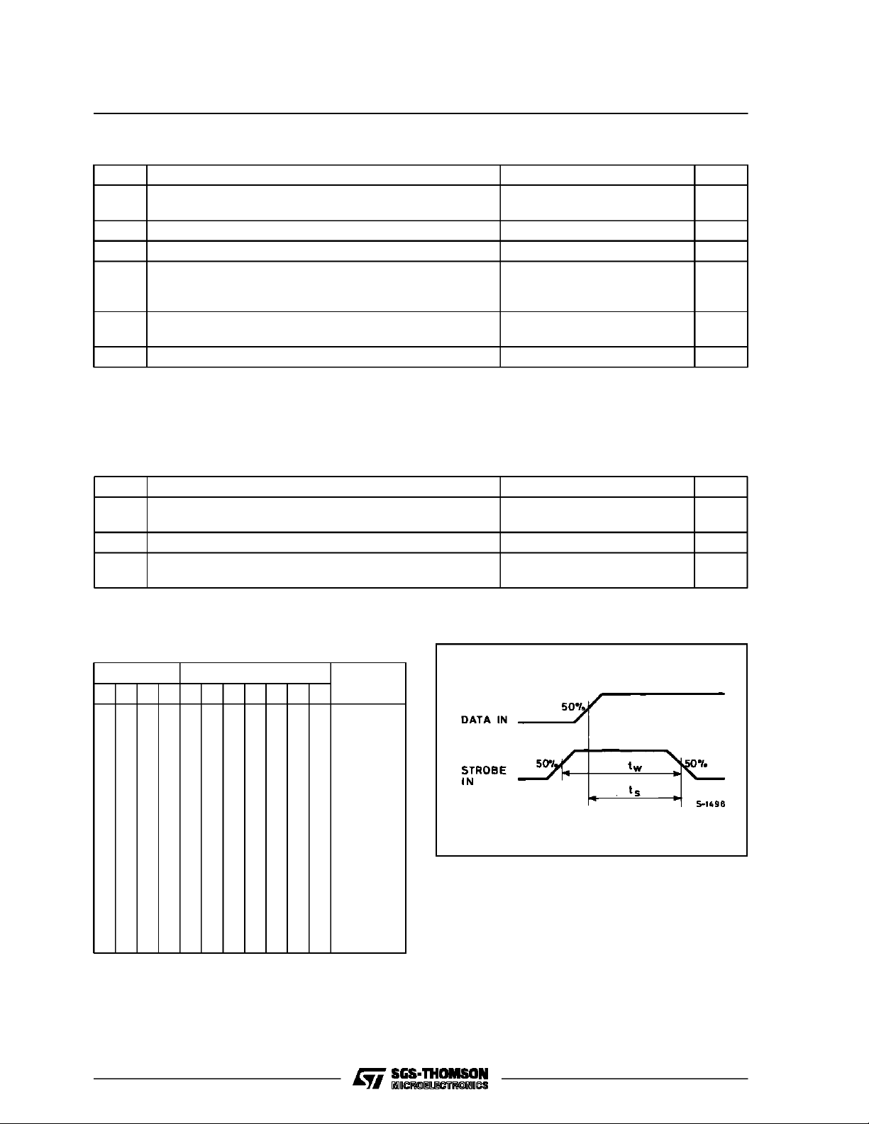
Data SetupTime and StrobePulse Duration.
Display
Character
0
1
2
3
4
5
6
7
8
9
L
H
P
A
–
BLANK
4/15
HCC/HCF4054B/55B/56B
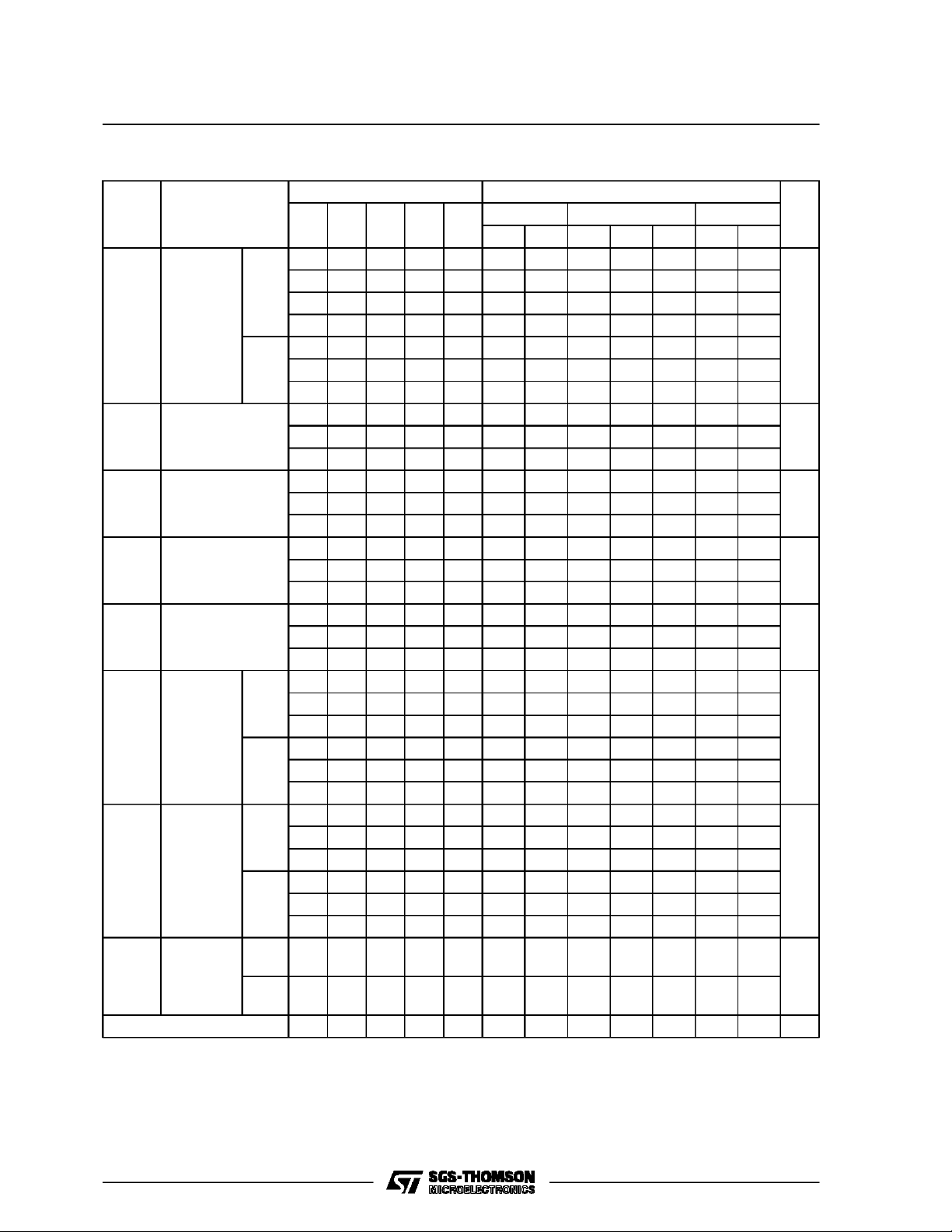
STATIC ELECTRICAL CHARACTERISTICS (over recommended operating conditions)
Test Conditions Value
Symbol Parameter
I
Quiescent
L
Supply
Current
HCC
Types
HCF
Types
V
OH
Output High
Voltage
V
OL
Output Low
Voltage
V
IH
Input High
Voltage
V
IL
Input Low
Voltage
I
OH
Output
High
Current
HCC
Types
HCF
Types
I
OL
Output
Low
Current
HCC
Types
HCF
Types
I
IH,IIL
** Input
Leakage
Current
HCC
Types
HCF
Types
CI** Input Capacitance 5 7.5 pF
*T
*T
** Any input.
=–55°CforHCC device : – 40°CforHCF device.
Low
= 125°CfrHCC device : + 85°C for HCF device.
High
TheNoise Marginfor both ”1” and ”0” levelis:1V min. with VDD= 5V,2V min. with VDD= 10V, 2.5 V min.with VDD=15V.
V
EEVI
(V) (V) (V) (V) (V)
VOVSSV
T
DD
* 25°CT
Low
Min. Max. Min. Typ. Max. Min. Max.
High
*
– 5 0/5 0 5 5 0.04 5 150
0 0/10 0 10 10 0.04 10 300
0 0/15 0 15 20 0.04 20 600
0 0/20 0 20 100 0.08 100 3000
– 5 0/5 0 5 20 0.04 20 150
0 0/10 0 10 40 0.04 40 300
0 0/15 0 15 80 0.04 80 600
0 0/5 0 5 4.95 4.95 4.95
0 0/10 0 10 9.95 9.95 9.95
0 0/15 0 15 14.95 14.95 14.95
0 5/0 0 5 0.05 0.05 0.05
0 10/0 0 10 0.05 0.05 0.05
0 15/0 0 15 0.05 0.05 0.05
–5
0.5/4.5
0 5 3.5 3.5 3.5
0 1/9 0 10 7 7 7
0
5
1.5/13.5
0.5/4.5
01511 11 11
0 5 1.5 1.5 1.5
0 9/1 0 10 3 3 3
0
1.5/13.5
015 4 4 4
– 5 0/5 4.5 0 5 – 0.6 – 0.45 – 0.9 – 0.3
0 0/10 9.5 0 10 – 0.6 – 0.45 – 0.9 – 0.3
0 0/15 13.5 0 15 – 1.9 – 1.5 – 3 – 1.1
– 5 0/5 4.5 0 5 – 0.47 – 0.38 – 0.9 – 0.28
0 0/10 9.5 0 10 – 0.47 – 0.38 – 0.9 – 0.28
0 0/15 13.5 0 15 – 1.58 – 1.27 – 3 – 0.95
– 5 0/5 0.4 0 5 1.6 1.3 2.6 0.9
0 0/10 0.5 0 10 1.6 1.3 2.6 0.9
0 0/15 1.5 0 15 4.2 3.4 6.8 2.4
– 5 0/5 0.4 0 5 1.37 1.1 2.6 0.82
0 0/10 0.5 0 10 1.37 1.1 2.6 0.82
0 0/15 1.5 0 15 3.62 2.9 6.8 2.17
–5
0 0/18 0 18 ± 0.1 ±10
0 0/15 0 15 ± 0.3 ±10
± 0.1 ± 1
–5
± 0.3 ± 1
Unit
µA
V
V
V
V
mA
mA
µA
µA
5/15
 Loading...