

SGS Thomson Microelectronics HCF4047B Datasheet
LOW-POWERMONOSTABLE/ASTABLE MULTIVIBRATOR
.LOW POWER CONSUMPTION : SPECIAL
COS/MOSOSCILLATOR CONFIGURATION
.MONOSTABLE(one-shot) OR ASTABLE (free-
running) OPERATION
.TRUE AND COMPLEMENTED BUFFERED
OUTPUTS
.ONLY ONEEXTERNAL R ANDC REQUIRED
.BUFFEREDINPUTS
.QUIESCENT CURRENT SPECIFIED TO 20V
FOR HCC DEVICE
.STANDARDIZED, SYMMETRICAL OUTPUT
CHARACTERISTICS
.5V, 10V, AND 15V PARAMETRIC RATINGS
.INPUT CURRENT OF 100nAAT18VAND 25°C
FOR HCC DEVICE
.100% TESTEDFOR QUIESCENTCURRENT
.MEETSALLREQUIREMENTSOFJEDECTEN-
TATIVESTANDARDN°13A,”STANDARDSPECIFICATIONS FOR DESCRIPTION OF ”B”
SERIESCMOS DEVICES”
HCC/HCF4047B
EY
(PlasticPackage)F(Ceramic Frit Seal Package)
M1
(MicroPackage)
ORDER CODES :
HCC4047BF HCF4047BM1
HCF4047BEY HCF4047BC1
(PlasticChipCarrier)
C1
DESCRIPTI ON
TheHCC4047B (extended temperature range) and
HCF4047B (intermediate temperature range) are
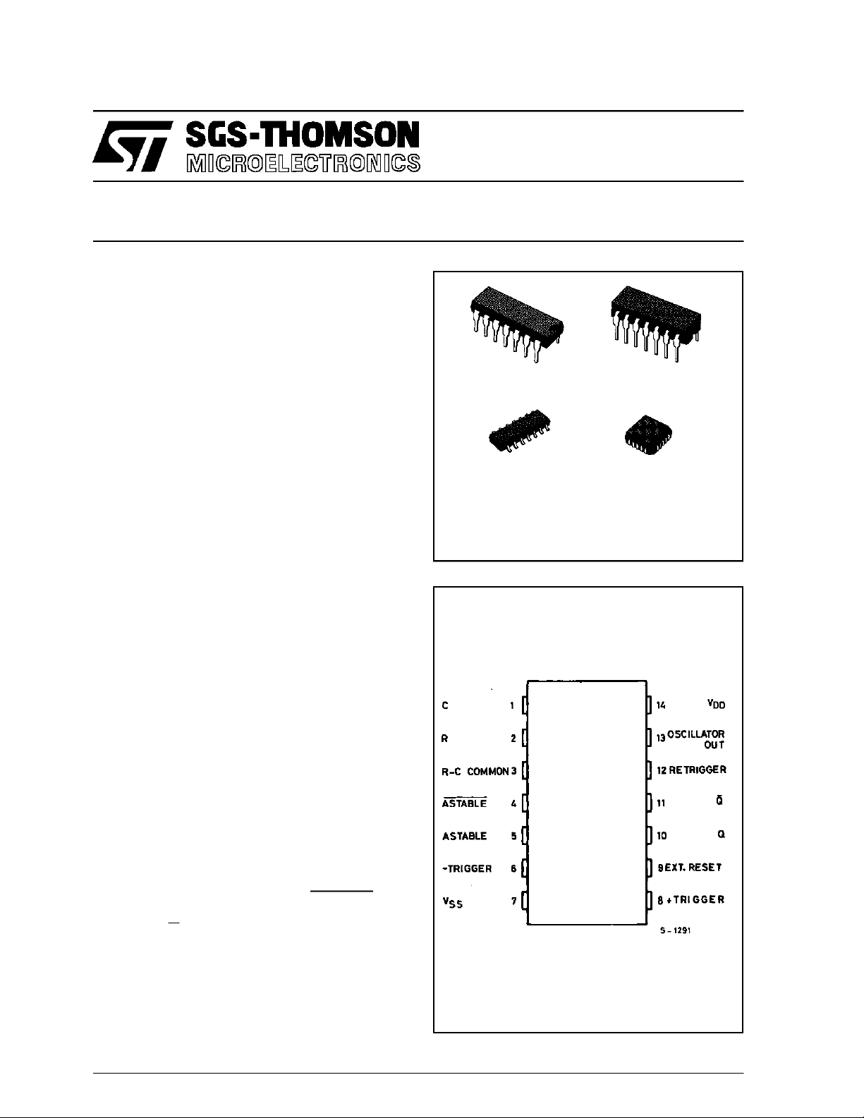
monolithic integrated circuits, available in 14-lead
dual in-line plastic or ceramic package and plastic micropackage. The HCC/HCF4047B consists of
a gatable astablemultivibrator with logictechniques
incorporated to permit positive or negative edgetriggeredmonostablemultivibratoractionwithretriggeringandexternal countingoptions. Inputsinclude
+TRIGGER-TRIGGER,ASTABLE, ASTABLE, RETRIGGER,and EXTERNAL RESET. Buffered outputs are Q, Q, and OSCILLATOR. In all modes of
operation, anexternalcapacitor mustbeconnected
betweenC-TimingandRC-Common terminals, and
an externalresistormust be connectedbetweenthe
R-TimingandRC-Commonterminals.Foroperating
modes see functional terminal connections and application notes.
PIN CONNECTIONS
June1989
1/15

HCC/HCF4047B
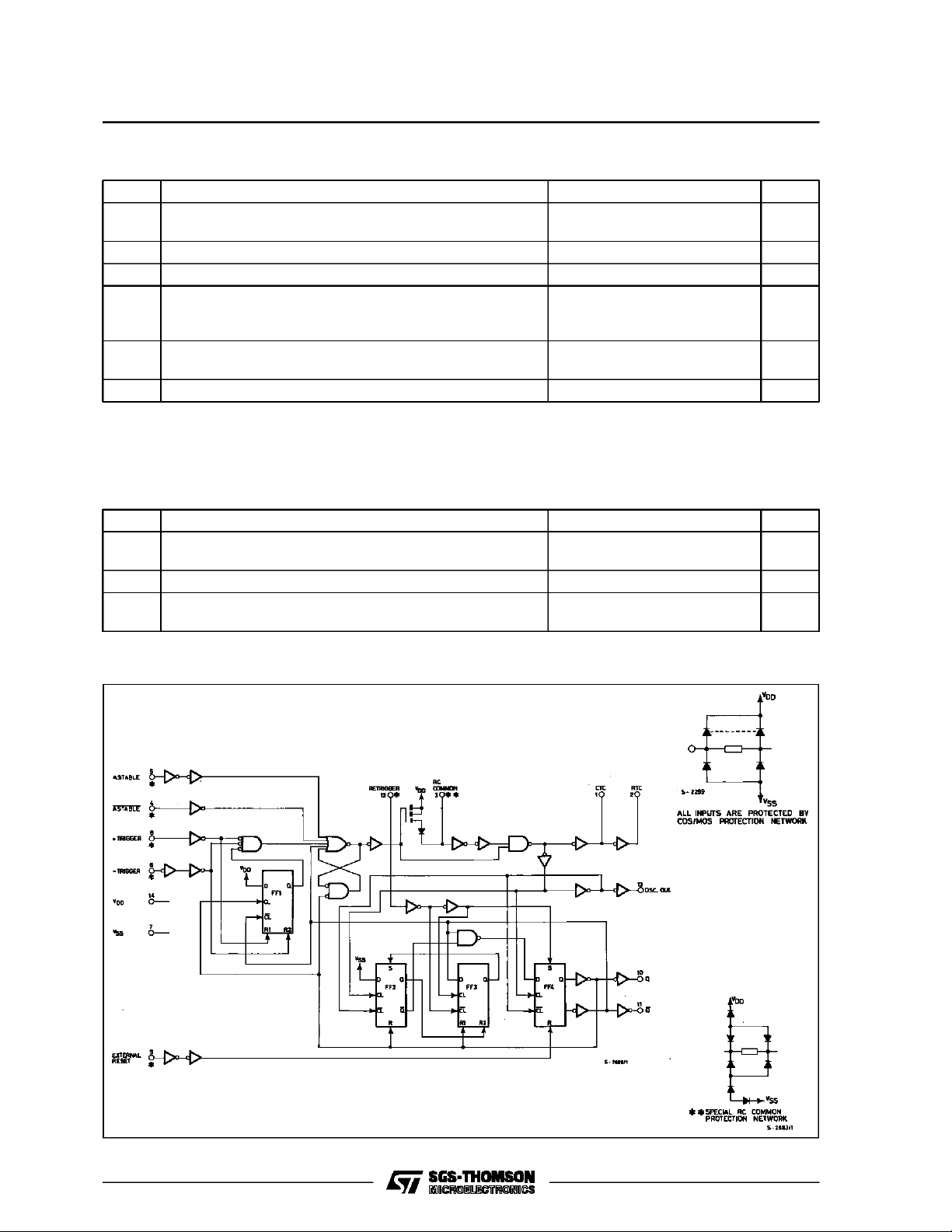
BLOCK DI AGRAM
FUNCTIONAL TERMINAL CONNECTIONS
Terminal Connections
Function*
to V
DD
to V
SS
Astable Multivibrator :
Free Running
True Gating
Complement Gating
4, 5, 6, 14
4, 6, 14
6, 14
7, 8, 9, 12
7, 8, 9, 12
5, 7, 8, 9 ,12
Monostable Multivibrator :
Positive–Edge Trigger
Negative–Edge Trigger
Retriggerable
External Countdown**
* In all cases external capacitor and resistor betweenpins, 1, 2 and 3 (see logic diagrams).
** Input pulse to Reset of External Counting Chip.
External Counting Chip Output to pin 4.
4, 14
4, 8, 14
4, 14
14
5, 6, 7, 9, 12
5, 7, 9, 12
5, 6, 7, 9
5, 6, 7, 8, 9, 12
Input
Pulse to
–
5
4
8
6
8, 12
–
Output
Pulse
From
10, 11, 13
10, 11, 13
10, 11, 13
10, 11
10, 11
10, 11
10, 11
Output Period
or
Pulse Width
t
(10, 11) = 4.40RC
A
t
(13) = 2.20RC
A
t
(10, 11) = 2.48RC
M
2/15
HCC/HCF4047B
ABSOLUTE MAXIMUM RATINGS
Symbol Parameter Value Unit
V
* Supply Voltage : HCC Types
DD
HCF Types
V
Input Voltage – 0.5 to VDD+ 0.5 V
i
I
DC Input Current (any one input) ± 10 mA
I
P
Total Power Dissipation (per package)
tot
Dissipation per Output Transistor
for T
= Full Package-temperature Range
op
T
Operating Temperature : HCC Types
op
HCF Types
T
Stresses above those listed under ”Absolute Maximum Ratings” may cause permanent damage to the device. This is a stress
rating only and functional operation of the device at these or any other conditions above those indicated in the operational sections
of this specification is not implied. Exposure to absolute maximum rating conditions for external periods may affect device reliability.
* All voltage values are referred to VSSpin voltage.
Storage Temperature – 65 to + 150 °C
stg
RECOMMENDED OPERATING CONDITIONS
Symbol Parameter Value Unit
V
T
Supply Voltage :HCC Types
DD
HCF Types
V
Input Voltage 0 to V
I
Operating Temperature : HCC Types
op
HCF Types
– 0.5 to + 20
– 0.5 to + 18
200
100
– 55 to + 125
–40to+85
3to18
3to15
DD
– 55 to + 125
–40to+85
V
V
mW
mW
°C
°C
V
V
V
°C
°C
LOGI C DIAGRAM
3/15
HCC/HCF4047B
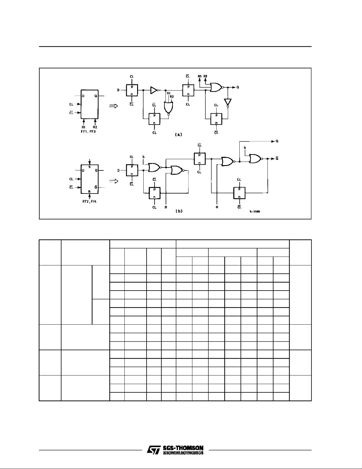
Detail for Flip-flopsFF1 and FF3(a) and for Flip-flops FF2 and FF4 (b).
STATIC ELECTRICAL CHARACTERISTICS (over recommended operating conditions)
Test Conditions Value
Symbol Parameter
Quiescent
I
L
Current
HCC
Types
HCF
Types
V
OH
Output High
Voltage
V
OL
Output Low
Voltage
V
IH
Input High
Voltage
*T
=–55°CforHCC device : – 40°CforHCF device.
Low
*T
= + 125°CforHCC device : + 85°CforHCF device.
High
The Noise Margin for both ”1” and ”0” level is : 1V min. with VDD= 5V, 2V min. with VDD= 10V, 2.5V min. with VDD= 15V.
V
V
I
(V) (V) (µA) (V)
O
|IO|V
DD
T
* 25°CT
Low
High
*
Min. Max. Min. Typ. Max. Min. Max.
0/ 5 5 1 0.02 1 30
0/10 10 2 0.02 2 60
0/15 15 4 0.02 4 120
0/20 20 20 0.04 20 600
0/ 5 5 4 0.02 4 30
0/10 10 8 0.02 8 60
0/15 15 16 0.02 16 120
0/ 5 < 1 5 4.95 4.95 4.95
0/10 < 1 10 9.95 9.95 9.95
0/15 < 1 15 14.95 14.95 14.95
5/0 < 1 5 0.05 0.05 0.05
10/0 < 1 10 0.05 0.05 0.05
15/0 < 1 15 0.05 0.05 0.05
0.5/4.5 < 1 5 3.5 3.5 3.5
1/9 < 1 10 7 7 7
1.5/13.5 < 1 15 11 11 11
Unit
µA
V
V
V
4/15

HCC/HCF4047B
STATIC ELECTRICAL CHARACTERISTICS (continued)
Test Conditions Value
Symbol Parameter
V
IL
Input Low
Voltage
I
OH
Output
Drive
Current
HCC
Types
HCF
Types
I
OL
Output
Sink
Current
HCC
Types
HCF
Types
I
IH,IIL
Input
leakage
Curent
HCC
Types
HCF
Types
C
Input Capacitance Any Input 5 7.5 pF
I
*T
=–55°C for HCC device : – 40°C for HCF device.
Low
*T
=+125°C for HCC device : + 85°C for HCF device.
High
The Noise Margin for both ”1” and ”0” level is : 1V min. with VDD= 5V, 2V min. with VDD= 10V, 2.5V min. with VDD= 15V.
V
V
I
(V) (V) (µA) (V)
O
|IO|V
DD
T
* 25°CT
Low
Min. Max. Min. Typ. Max. Min. Max.
4.5/0.5 < 1 5 1.5 1.5 1.5
9/1 < 1 10 3 3 3
13.5/1.5 < 1 15 4 4 4
0/ 5 2.5 5 – 2 – 1.6 – 3.2 – 1.15
0/ 5 4.6 5 – 0.64 – 0.51 – 1 – 0.36
0/10 9.5 10 – 1.6 – 1.3 – 2.6 – 0.9
0/15 13.5 15 – 4.2 – 3.4 – 6.8 – 2.4
0/ 5 2.5 5 – 1.53 – 1.36 – 3.2 – 1.1
0/ 5 4.6 5 – 0.52 – 0.44 – 1 – 0.36
0/10 9.5 10 – 1.3 – 1.1 – 2.6 – 0.9
0/15 13.5 15 – 3.6 – 3.0 – 6.8 – 2.4
0/ 5 0.4 5 0.64 0.51 1 0.36
0/10 0.5 10 1.6 1.3 2.6 0.9
0/15 1.5 15 4.2 3.4 6.8 2.4
0/ 5 0.4 5 0.52 0.44 1 0.36
0/10 0.5 10 1.3 1.1 2.6 0.9
0/15 1.5 15 3.6 3.0 6.8 2.4
0/18
18
± 0.1 ±10
–5
± 0.1
Any Input
0/15
15 ± 0.3 ±10
–5
± 0.3 ± 1
High
*
± 1
Unit
V
mA
mA
µA
DYNAMIC ELECTRICAL CHARACTERISTICS (T
=25°C, CL= 50pF, RL= 200kΩ,
amb
typical temperature coefficient for all VDDvalues is 0.3%/°C, all input rise and fall times = 20ns)
Symbol Parameter
t
PLH,tPHL
Propagation
Delay Time
Astable, Astable to
osc. out
Astable, Astable to
Q, Q
+ or – Trigger to
Q, Q
Test Conditions
(V) Min. Typ. Max.
V
DD
5 200 400
10 100 200
15 80 160
5 350 700
10 175 350
15 125 250
5 500 1000
10 225 450
15 150 300
Value
Unit
ns
5/15
 Loading...