

SGS Thomson Microelectronics HCF4044B, HCF4043B Datasheet
QUAD N OR R-S LATC H-4043B
QUAD N AND R-S LATC H-4 044B
.QUIESCENT CURRENT SPECIFIED TO 20V
FOR HCC DEVICE
.3-LEVEL OUTPUTS WITHCOMMON OUTPUT
ENABLE
.SEPARATE SET AND RESET INPUT FOR
EACHLATCH
.5V, 10V,AND 15V PARAMETRIC RATINGS
.NOR AND NAND CONFIGURATIONS
.INPUT CURRENTOF 100nAAT18V AND 25°C
FOR HCC DEVICE
.100% TESTEDFOR QUIESCENTCURRENT
.MEETSALLREQUIREMENTSOFJEDECTEN-
TATIVESTANDARDN°13A,”STANDARDSPECIFICATIONS FOR DESCRIPTION OF ”B”
SERIESCMOS DEVICES”
HCC/HCF4043B
HCC/HCF4044B
QUAD 3-STATER-S LATCHES
EY
(Plastic Package)
M1
(MicroPackage)
ORDER CODES :
HCC40XXBF HCF40XXBM1
HCF40XXBEY HCF40XXBC1
(CeramicFrit Seal Package)
(Plastic Chip Carrier)
F
C1
DESCRIPTI ON
The HCC4043B, HCC4044B, (extended tempera-
ture range) and the HCF4043B, HCF4044B (inter-
mediate temperature range) are monolithic
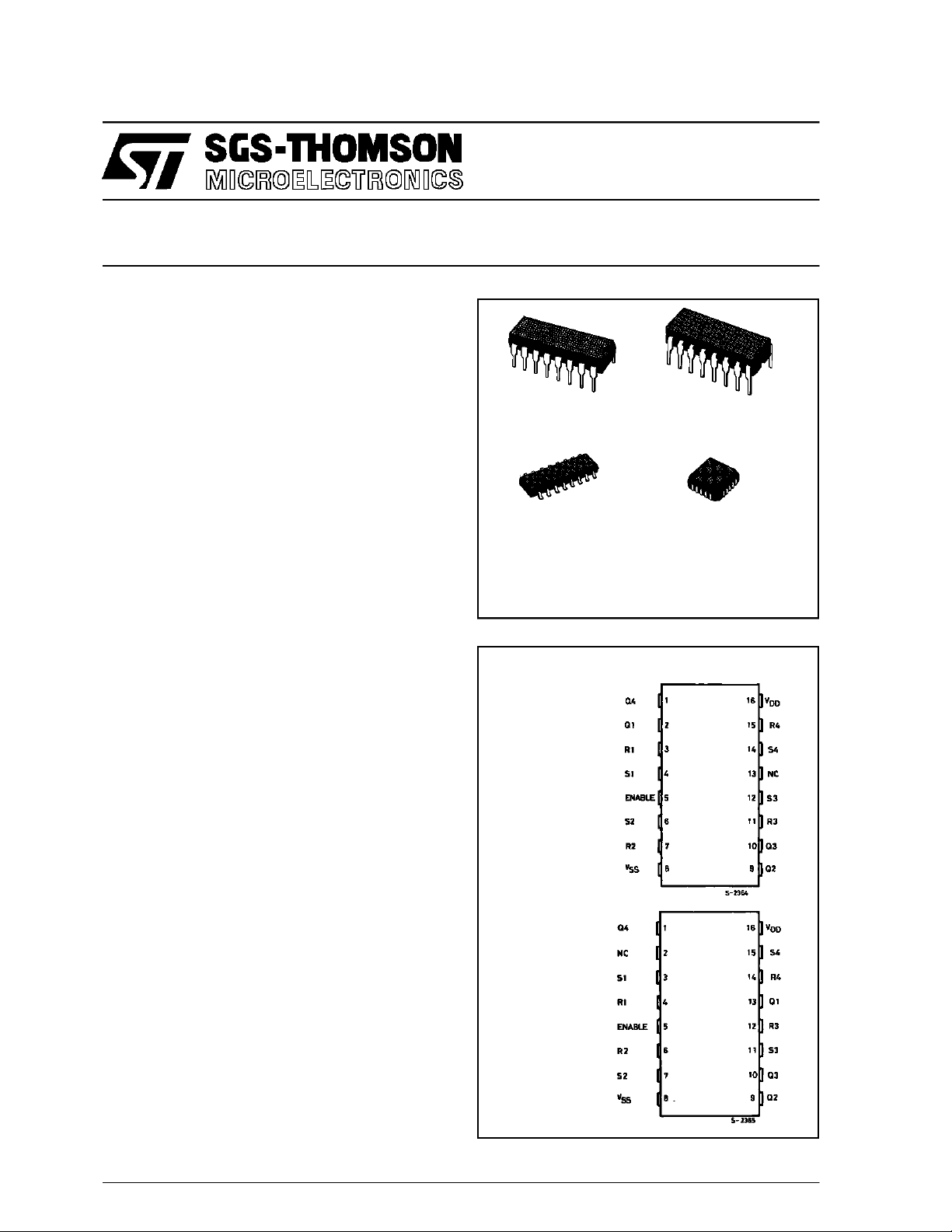
integrated circuits, available in 16-lead dual in-line
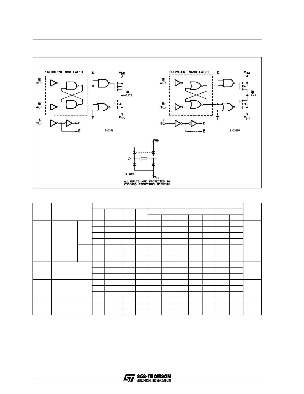
plastic or ceramic package and plastic micropackage. The HCC/HCF4043B types are quad cross-
coupled 3-state COS/MOS NOR latches and the
HCC/HCF4044B types are quad cross-coupled 3state COS/MOS NAND latches. Each latch has a
separate Q output and individual SET and RESET
inputs. The Q outputs are controlledby a common
ENABLE input.A logic”1” or”high” onthe ENABLE
input connectsthe latch states to theQ outputs. A
logic ”0” or”low” on the ENABLEinput disconnects
the latch states from the Q outputs, resulting in an
open circuit condition on the Q outputs. The open
circuit feature allows common bussing of the outputs.
PIN C ONN ECT IONS
4043B
4044B
June1989
1/13

HCC/HCF4043B/4044B
FUN CTIONAL DIAG R A MS
4043B 4044B
ABSOLUTE MAXIMUM RATIN GS
Symbol Parameter Value Unit
V
* Supply Voltage :HC C Types
DD
HCF Types
V
Input Voltage – 0.5 to VDD+ 0.5 V
i
I
DC Input Current (any one input) ± 10 mA
I
P
Total Power Dissipation (per package)
tot
Dissipation per Output Transistor
for Top= Full Package-temperature Range
T
Operating Temperature : HCC Types
op
HCF Types
T
Stresses above those listed under ”Absolute Maximum Ratings” may cause permanent damage to the device. This is a stress
rating only and functional operation of the device at these or any other conditions above those indicated in the operational sections
of this specification is not implied. Exposure to absolute maximum rating conditions for external periods may affect device reliability.
* All voltage values are referred to VSSpin voltage.
Storage Temperature – 65 to + 150 °C
stg
– 0.5 to + 20
– 0.5 to + 18
200
100
– 55 t o + 125
–40to+85
V
V
mW
mW
°C
°C
RECOMMENDED OPERATING CONDITIONS
Symbol Parameter Value Unit
V
T
2/13
Supply Voltage :HC C Types
DD
HCF Types
V
Input Voltage 0 to V
I
Operating Temperature : HCC Types
op
HCF Types
3to18
3to15
DD
– 55 t o + 125
–40to+85
V
V
V
°C
°C
LOGI C DI AGRAMS
HCC/HCF4043B/4044B
4044B 4043B
STATIC ELECTRICAL CHARACTERISTICS (over recommended operatingconditions)
Test Conditions Valu e
Symbol Parameter
(V) (V) (µA) (V)
I
L
Quiescent
Current
HCC
Types
0/ 5 5 1 0.02 1 30
0/10 10 2 0.02 2 60
0/15 15 4 0.02 4 120
0/20 20 20 0.04 20 600
HCF
Types
OH
Output High
V
Voltage
0/ 5 5 4 0.02 4 30
0/10 10 8 0.02 8 60
0/15 15 16 0.02 16 120
0/ 5 < 1 5 4.95 4.95 4.95
0/10 < 1 10 9.95 9.95 9.95
0/15 < 1 15 14.95 14.95 14.95
V
OL
Output Low
Voltage
5/0 < 1 5 0.05 0.05 0.05
10/0 < 1 10 0.05 0.05 0.05
15/0 < 1 15 0.05 0.05 0.05
IH
Input High
V
Voltage
*T
=–55°CforHCC device : – 40°CforHCF device.
Low
*T
= + 125°CforHCC device : + 85°CforHCF device.
High
The Noise Margin for both ”1” and ”0” level is : 1V min. with VDD= 5V, 2V min. with VDD= 10V, 2.5V min. with VDD= 15V.
V
V
I
O
|IO|V
DD
T
* 25°CT
Low
Min. Max. Min. Typ. M ax. Min. Max.
0.5/4.5 < 1 5 3.5 3.5 3.5
1/9 < 1 10 7 7 7
1.5/13.5 < 1 15 11 11 11
High
*
Unit
µA
V
V
V
3/13
HCC/HCF4043B/4044B
STATIC ELECTRICAL CHARACTERISTICS (continued)
Test Conditions Valu e
Symbol Parameter
(V) (V) (µA) (V)
IL
Input Low
V
Voltage
I
OH
Output
Drive
Current
HCC
Types
0/ 5 2.5 5 – 2 – 1.6 – 3.2 – 1.15
0/ 5 4.6 5 – 0.64 – 0.51 – 1 – 0.36
0/10 9.5 10 – 1.6 – 1.3 – 2.6 – 0.9
0/15 13.5 15 – 4.2 – 3.4 – 6.8 – 2.4
0/ 5 2.5 5 – 1.53 – 1.36 – 3.2 – 1.1
HCF
Types
0/ 5 4.6 5 – 0.52 – 0.44 – 1 – 0.36
0/10 9.5 10 – 1.3 – 1.1 – 2.6 – 0.9
0/15 13.5 15 – 3.6 – 3.0 – 6.8 – 2.4
OL
Output
Sink
Current
HCC
Types
I
HCF
Types
I
IH,IIL
Input
leakage
Current
HCC
Types
HCF
Types
I
OH
3-state
Output
HCC
Types
HCF
Types
Input Capacitance Any Input 5 7.5 pF
C
I
*T
=–55°CforHCC device : – 40°CforHCF device.
Low
*T
= + 125°CforHCC device : + 85°CforHCF device.
High
The Noise Margin for both ”1” and ”0” level is : 1V min. with VDD= 5V, 2V min. with VDD= 10V, 2.5V min. with VDD= 15V.
0/ 5 0.4 5 0.64 0.51 1 0.36
0/10 0.5 10 1.6 1.3 2.6 0.9
0/15 1.5 15 4.2 3.4 6.8 2.4
0/ 5 0.4 5 0.52 0.44 1 0.36
0/10 0.5 10 1.3 1.1 2.6 0.9
0/15 1.5 15 3.6 3.0 6.8 2.4
0/18
0/15
0/18 0/18 18 ± 0.4 ±10
0/15 0/15 15 ± 1.0 ±10
V
V
I
O
|IO|V
DD
T
* 25°CT
Low
Min. Max. Min. Typ. M ax. Min. Max.
4.5/0.5 < 1 5 1.5 1.5 1.5
9/1 < 1 10 3 3 3
13.5/1.5 < 1 15 4 4 4
18 ± 0.1 ±10
–5
± 0.1 ± 1
Any Input
15 ± 0.3 ±10
–5
± 0.3 ± 1
–4
± 0.4 ± 12
–4
± 1.0 ± 7.5
High
*
Unit
V
mA
mA
µA
µA
DYNAMIC ELECTRICAL CHARACTERISTICS (T
=25°C, CL= 50pF, RL= 200kΩ,
amb
typical temperature coefficient for all VDDvalues is 0.3%/°C, all input rise and fall times = 20ns)
Symbol Parameter
t
PLH,tPHL
Propagation Delay Time
(SET or RESET to Q)
t
PZH,tPHZ
3-state Propagation Delay Time
(ENABLE to Q)
4/13
Test Co n di t i ons Value
V
(V) Min. Typ. Max.
DD
5150300
10 70 140
15 50 100
5115230
10 55 110
15 40 80
Unit
ns
ns
 Loading...