

8-BIT MICROCOMPUTER UNIT
HARDWAR E FEATU RES DESCRIPTI O N
.32 TTL/CMOSCOMPATIBLE I/O LINES
.24 BIDIRECTIONAL (8 lines are LED compati-
ble)
.8 INPUT-ONLY
.3776 BYTES OF USER ROM
.112 BYTES OF RAM
.SELF-CHECK MODE
.ZERO-CROSSINGDETECT/INTERRUPT
.INTERNAL 8-BIT TIMER WITH 7-BIT SOFT-
WARE PROGRAMMABLE PRESCALER AND
CLOCKSOURCE
The EF6805U3 Microcomputer Unit (MCU) is a
member of the 6805 Family of low-costsingle-chip
Microcomputers. The 8-bit microcomputer contains
a CPU, on-chip CLOCK, ROM, RAM, I/O, and TIMER.It is designed for the userwho needs an economical microcomputer withtheproven capabilities
of the 6800-based instruction set. A comparison of
thekey featuresofseveral members ofthe 6805Family of Microcomputers is shown at the end of this
data sheet.The following are someof the hardware
and softwarehighlights of the EF6805U3 MCU.
.5V SINGLE SUPPLY
SOFTWARE FEATURES
.10 POWERFUL ADDRESSINGMODES
.BYTE EFFICIENT INSTRUCTION SET WITH
TRUE BIT MANIPULATION, BIT TEST, AND
BRANCHINSTRUCTIONS
.SINGLE INSTRUCTION MEMORY EXA-
MINE/CHANGE
.POWERFUL INDEXED ADDRESSING FOR
TABLES
.FULL SET OF CONDITIONALBRANCHES
.MEMORYUSABLE AS REGISTER/FLAGS
.COMPLETE DEVELOPMENT SYSTEM SUP-
PORTON INICE
USER SELECTAB LE OPTIONS
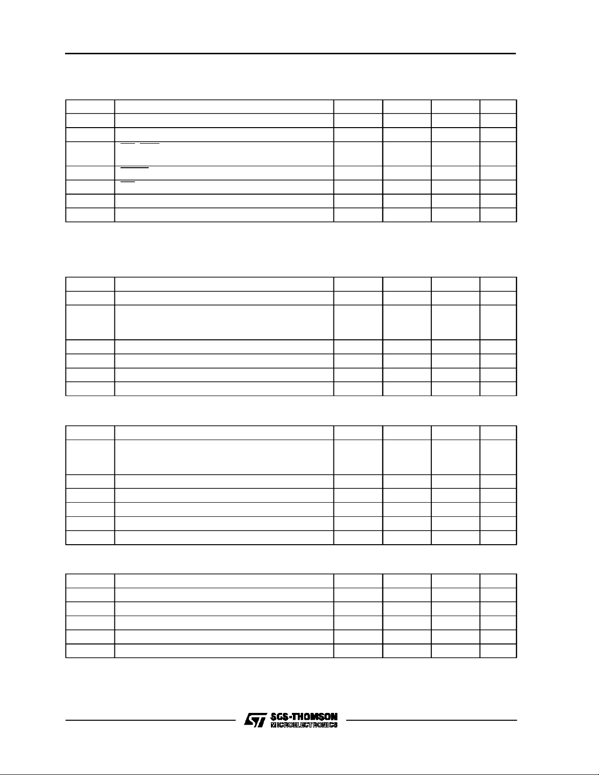
PIN CONNECTIONS
.8 BIDIRECTIONAL I/O LINES WITH TTL OR
TTL/CMOSINTERFACE OPTION
.8 BIDIRECTIONALI/O LINES WITHTTL ORO-
PEN-DRAIN INTERFACEOPTION
.CRYSTALOR LOW-COST RESISTOR OSCIL-
LATOROPTION
.LOWVOLTAGE INHIBIT OPTION
.VECTORED INTERRUPTS : TIMER, SOFT-
WARE, AND EXTERNAL
.USER CALLABLE SELF-CHECK SUBROU-
TINES
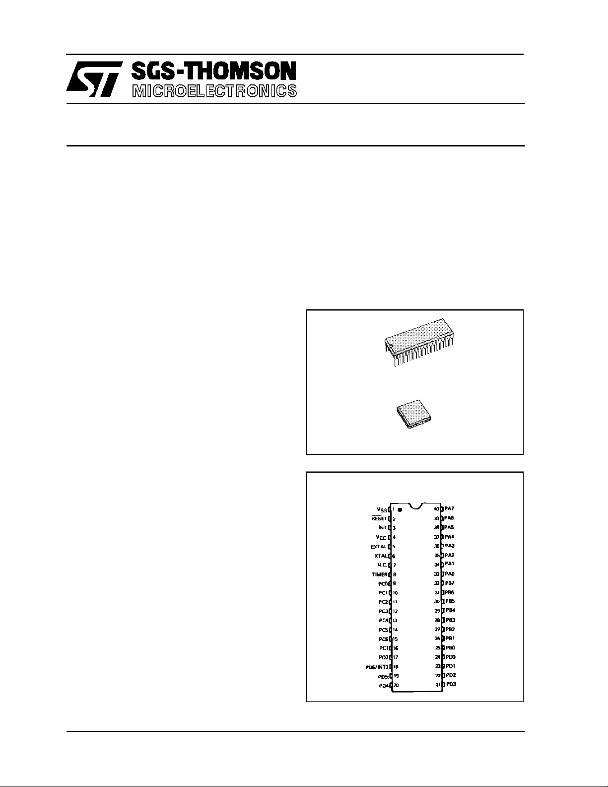
EF6805U3
1
P
(PDIP40)
FN
(PLCC44)
March1989
1/31

EF6805U3
Figure 1 : EF6805U3 HMOS Microcomputer BlockDiagram.
ABSOLUTEMAXIMUM RATINGS
Symbol Parameter Value Unit
V
CC
V
in
Supply Voltage – 0.3 to + 7.0 V
Input Voltage (except TIMER in self-check mode and
– 0.3 to + 7.0 V
open-drain inputs)
V
in
T
A
T
stg
T
This device contains circuitry to protect the inputs against damage due to high static voltages or electrical fields, however, it is advised
that normal precautions be taken to avoid application of any voltage higher than maximum rated voltages to this high impedance circuit.
For proper operation it is recommended that Vinand V
hanced if unused inputs except EXTAL are tied to an appropriate logic voltage level (e.g., either VSSor VCC).
Input Voltage (open-drain pins, TIMER pin in self-check mode) – 0.3 to + 15.0 V
Operating Temperature Range
(T
to TH)
L
VSuffix
TSuffix
0to+70
–40to+85
– 40 to + 105
Storage Temperature Range – 55 to + 150 °C
Junction Temperature
j
Plastic Package
PLCC
be constrained to the range VSS(Vinor V
out
150
150
. Reliability of operation is en-
out)VCC
°C
°C
THERMALDATA
θ
JA
Thermal Resistance
Plastic
PLCC
50
80
°C/W
2/31

EF6805U3
POW ER CO NSIDE R ATIONS
Theaverage chip-junctiontemperature,TJ, inCcan
be obtainedfrom :
TJ=TA+(PD.JA) (1)
Where :
TA= AmbientTemperature, C
JA=Package ThermalResistance,Junction-to-Ambient,C/W
PD=P
INT+PPORT
P
INT=ICCxVCC
P
= Port Power Dissipation, Watts - User De-
PORT
, Watts - Chip Internal Power
termined
For most applications P
glected. P
maybecomesignificant if thedevice
PORT
PORTPINT
and can be ne-
is configured to drive Darlington bases or sink LED
loads.
An approximate relationship between PDandTJ(if
P
is neglected) is :
PORT
PD=K+(TJ+273C) (2)
Solving equations 1 and2 forK gives :
K=PD.(TA+273C) + JA.P
2
(3)
D
Where K is a constant pertaining to the particular
part.K can be determined from equation 3 bymeasuring PD(atequilibrium) for a known TA. Usingthis
valueof K the values of PDandTJcanbe obtained
by solving equations (1) and (2) iteratively for any
valueof TA.
ELECTRICAL CHARACTERISTICS(VCC= + 5.25Vdc ± 0.5Vdc, VSS= 0Vdc, TA=TLto THunless
otherwise noted)
Symbol Parameter Min. Typ. Max. Unit
V
IH
V
IH
V
IL
V
IRES +
V
IRES –
V
INT
P
D
C
in
V
LVR
VL
I
in
* Due to internal biasing this input (when unused) floats to approximately 2.2V.
Input High Voltage
RESET (4.75 ≤ V
(VCC< 4.75)
INT (4.75 ≤ V
(VCC< 4.75)
All Other (except timer)
CC
≤ 5.75)
CC
≤ 5.75)
4.0
– 0.5
V
CC
4.0
V
– 0.5
CC
•
•
2.0
Input High Voltage Timer
Timer Mode
Self-check Mode
2.0
9.0 10.0
Input Low Voltage
RESET
INT
All Other
V
SS
V
SS
V
SS
•
RESET Hystereris Voltages (see figures 10, 11 and 12)
”Out of Reset”
”Into Reset”
INT Zero Crossing Input Voltage, Through a
2.1
0.8
24V
Capacitor
Power Dissipation - (no port loading, VCC= 5.75V)
TA=0°C
TA=–40°C
520
580
Input Capacitance
EXTAL
All Other
25
10
Low Voltage Recover 4.75 V
Low Voltage Inhibit 2.75 3.75 4.70 V
VI
Input Current
TIMER (V
INT (Vin= 2.4V to VCC)
EXTAL (V
= 0.4V)
in
= 2.4V to VCC- crystal option)
in
20
(Vin= 0.4V - crystal option)
RESET (Vin= 0.8V) - External Capacitor Charging
– 40.0
Current
V
V
V
V
V
V
CC
15.0
0.8
1.5
0.8
4.0
2.0
740
800
20
50
10
– 1600
–40
CC
CC
CC
CC
CC
+ 1.0
V
V
V
V
ac p-p
mW
pF
µA
3/31
EF6805U3
SWITCHING CHARACTERISTICS
(VCC= + 5.25Vdc ± 0.5Vdc, VSS= 0Vdc, TA=TLto THunless otherwise noted)
Symbol Parameter Min. Typ. Max. Unit
f
osc
t
cyc
t
WL,tWH
t
RWL
f
INT
PORT ELECTRICAL CHARACTERISTICS
(VCC= + 5.25Vdc ± 0.5Vdc, VSS= 0Vdc, TA=TLto THunless otherwise noted)
PORT A WITH CMOS DRIVEENABLED
Symbol Parameter Min. Typ. Max. Unit
V
OL
V
OH
V
IH
V
IL
I
IH
I
IL
Oscillator Frequency 0.4 4.2 MHz
Cycle Time (4/f
INT, INT2, and TIMER Pulse Width (see interrupt
) 0.95 10 µs
osc
t
+ 250 ns
cyc
section)
RESET Pulse Width t
+ 250 ns
cyc
INT Zero-crossing Detection Input Frequency 0.03 1 kHz
External Clock Input Duty Cycle (EXTAL) 40 50 60 %
Crystal Oscillator Start-up Time* 100 ms
Output Low Voltage (I
= 1.6mA) 0.4 V
Load
Output High Voltage
I
= – 100µ A
Load
I
=– 10µA
Load
Input High Voltage (I
Input Low Voltage (I
= – 300µA max.) 2.0 V
Loa d
= – 500µA max.) V
Load
2.4
VCC– 1.0
SS
CC
0.8 V
High Z State Input Current (Vin= 2.0V to VCC) – 300 µA
High Z State Input Current (Vin= 0.4V) – 500 µA
V
V
PORT B
Symbol Parameter Min. Typ. Max. Unit
V
OL
V
OH
I
OH
V
IH
V
IL
I
TSI
Output Low Voltage
I
= 3.2mA
Loa d
I
= 10mA (sink)
Loa d
Output High Voltage I
=– 200µA 2.4 V
Load
0.4
1.0
Darlington Current Drive (source) VO= 1.5V – 1.0 – 10 mA
Input High Voltage 2.0 V
Input Low Voltage V
SS
CC
0.8 V
High Z State Input Current < 2 10 µA
PORT C AND PORT A WITH CMOS DRIVE DISABLED
Symbol Parameter Min. Typ. Max. Unit
V
OL
V
OH
V
IH
V
IL
I
TSI
Output Low Voltage I
Output High Voltage I
Input High Voltage 2.0 V
Input Low Voltage V
= 1.6mA 0.4 V
Load
= – 100µA 2.4 V
Load
CC
SS
0.8 V
High Z State Input Current < 2 10 µs
V
V
V
4/31
EF6805U3
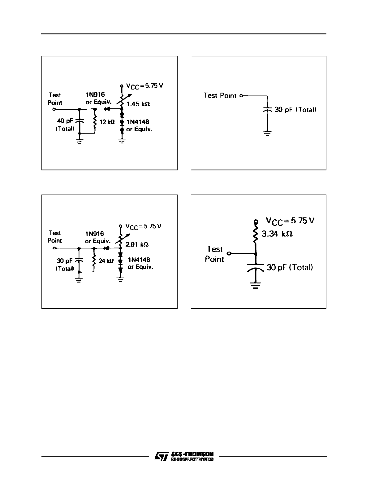
Figure 2 : TTL Equivalent Test Load (port B). Figure3 :CMOS Equivalent Test Load (port A).
Figure 4 : TTL Equivalent Test Load (port A
andC).
SIGNAL DESCRIPTION
The input and output signals for theMCU,shown in
figure 1, are described in the following paragraphs.
VCCANDVSS-Power is supplied to the MCU using
thesetwopins. VCCispower and VSSis the ground
connection.
INT - This pin provides the capability for asynchronously applying an external interrupt to the MCU.
Refer to Interrupts Section for additional information.
XTALAND EXTAL - These pins provide controlinput for theon-chip clockoscillator circuit. A crystal,
a resistor, or an external signal, depending on user
selectable manufacturing mask option, can be
connected to these pins to provide a system clock
withvariousdegreesof stability/costtradeoffs.Lead
Figure 5 : Open-drain Equivalent Test Load (port
C).
length and stray capacitance on these two pins
should be minimized. Refer to InternalClock Generator Options Section for recommendations about
these inputs.
NOTE : Pin 7 in DIL package/pin 8 in PLCC
package is connected to internal protection.
TIMER- The pinallowsan externalinputto be used
to control the internal timer circuitry and also to initiatetheselftestprogram. Referto TimerSection for
additional information about the timer circuitry.
RESET - This pin allows resetting of the MCU at
times other than the automatic resetting capability
already in the MCU. The MCUcan be resetby pulling RESET low. Refer to Resets Section for additionalinformation.
5/31
EF6805U3
INPUT/OUTPUTLINES(PA0-PA7, PB0-PB7,PC0PC7, PD0-PD7) - These32 liens arearranged into
four 8-bit ports (A, B, C, and D). Ports A, B, and C
areprogrammable as eitherinputs oroutputs under
software control of the data direction registers
(DDRs).Port D is for digital input only and bit 6 may
be used for a second interrupt INT2. Refer to Input/OutputSectionand Interrupts Section for additional information.
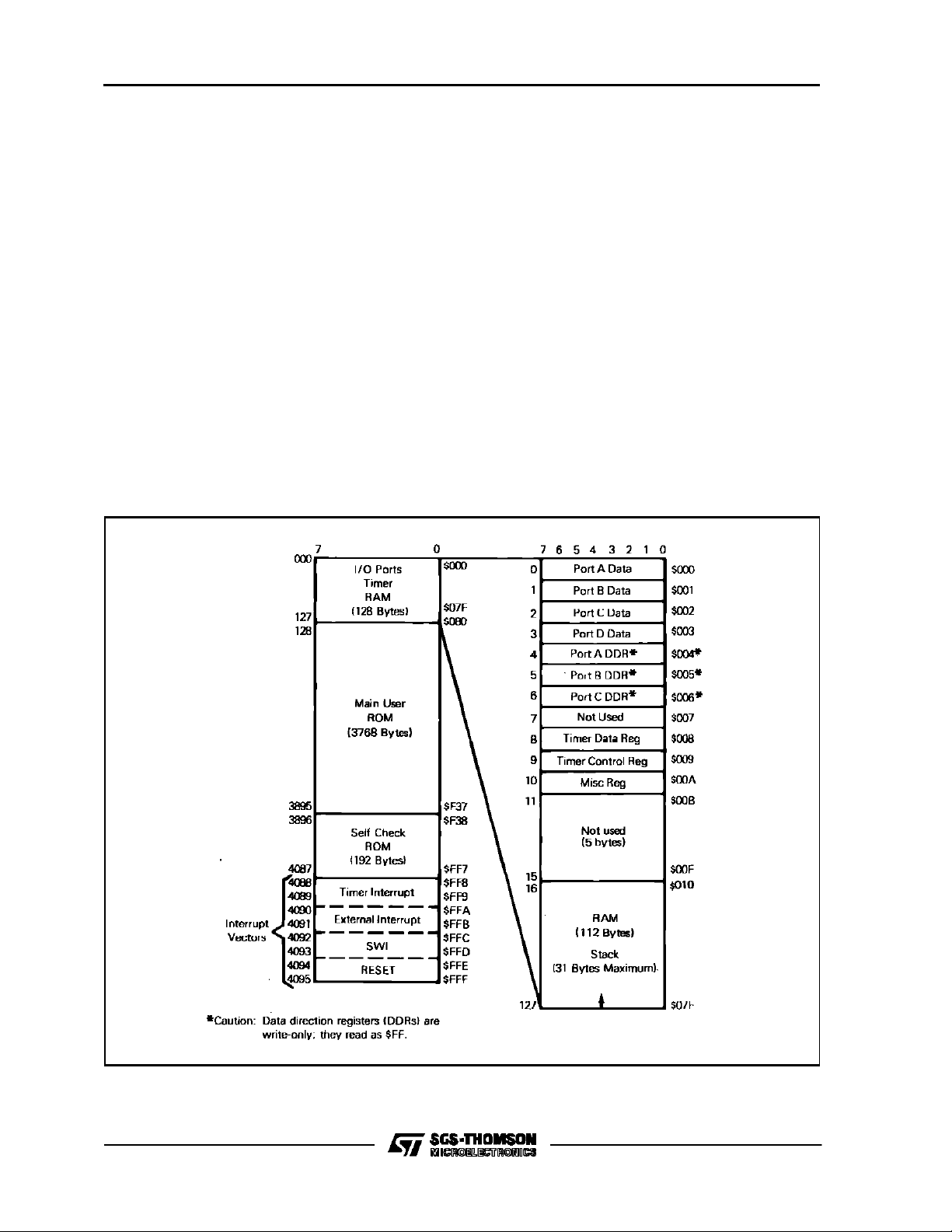
MEMORY-TheMCUiscapable ofaddressing4096
bytes of memory and I/O registers with its program
counter. The EF6805U3 MCU has implemented
4090 of these bytes. This consists of : 3776 user
ROM bytes, 192 self-check ROM bytes, 112 user
RAM bytes, 7 portI/O bytes, 2 timerregisters, and
a miscellaneous register ; see figure 6 for the Address map. The user ROM has been split into two
areas. The main user ROM area is from $080 to
$F37. The last 8 userROM locationsat the bottom
of memory are for the interrupt vectors.
Figure 6 : EF6805U3 MCU Address Map.
TheMCUreservesthefirst-16memorylocationsfor
I/O features, of which 10 have been implemented.
These locations are used for the ports, the port
DDRs,the timer and the INT2miscellaneous register, and the 112 RAM bytes, 31 bytes are shared
with the stack area. The stack must be used with
carewhen data shares thestack area.
Thesharedstackareaisusedduringtheprocessing
of an interrupt or subroutine calls to save the
contents of the CPUstate. The register contents are
pushed onto the stack in the order shown in figure
7. Since the stack pointer decrements during
pushes, the low order byte (PCL) of the program
counter is stackedfirst, then the high order fourbits
(PCH)are stacked.This ensures that the program
counter is loaded correctly during pulls from the
stack since the stack pointer increments when it
pulls data from the stack. A subroutine call results
in only the program counter (PCL, PCH) contents
beingpushed onto thestack ;theremaining CPUregistersare not pushed.
* Caution : Data direction registers (DDRs) are write only, they read as $FF.
6/31
EF6805U3
Figure 6 : Interrupt Stacking Order.
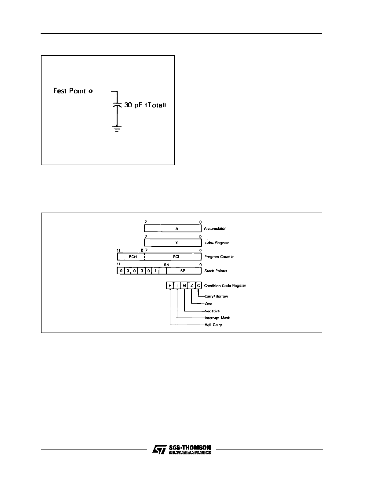
CENTRAL P ROC ESSIN G U NI T
The CPU of theEF6805 Family is implemented independently from the I/O or memory configuration.
Figure 8 : Programming Model.
Consequently, it can be treated as an independent
central processor communicating with I/O and memory via internal address, data, and control buses.
REGISTERS
The 6805 FamilyCPUhasfiveregistersavailable to
the programmer. Theyareshowninfigure8 andare
explained in the following paragraphs.
ACCUMULATOR(A)-Theaccumulatoris ageneral
purpose 8-bitregisterusedto holdoperandsandresults of arithmetic calculations or data manupulations.
INDEX REGISTER(X) - The index register is an 8bit register usedfor the indexed addressing mode.
It contains an 6-bit value that may be added to an
instruction value tocreate aneffectiveaddress. The
indexregister can also be used for data manipulations using the read-modify-write instructions. The
Index Register may also be used as a temporary
storagearea.
PROGRAMCOUNTER (PC) - The Program Counter is a 12 bit registerthat contains th address of the
next instructionto be executed.
STACK POINTER(SP) - The stackpointer is a 12bitregisterthatcontains the address of thenextfree
location on the stack. During an MCU reset or the
resetstackpointer(RSP)instruction, thestackpointer is set to location$07F. The stackpointer is then
decremented as data is pushed onto the stack and
incremented asdata is then pulled from the stack.
The seven most significant bits of the stack pointer
are permanently set to 0000011. Subroutines and
interrupts maybe nested down tolocation $061(31
bytes maximum) which allows the programmer to
use up to 15 levelsof subroutine calls (less if interrupts are allowed).
CONDITIONCODE REGISTER(CC) - The conditioncoderegisterisa5-bitregisterin whichfoourbits
areusedto indicate theresultsof the instructionjust
executed. Thesebitscan be individually tested by a
program andspecificactiontakenasaresult oftheir
state. Each bit is explained in the following paragraphs.
7/31

EF6805U3
HalfCarry(H) -Setduring ADDandADCoperations
to indicate that a carry occurred betweenbits3 and
4.
Interrupt(I) - Whenthisbitis set, the timeran exter-
nalinterrupts(INTandINT2)are masked(disabled).
Ifaninterruptoccurswhile thisbitisset,the interrupt
is latchedandis processed as soonas the interrupt
bitis cleared.
Negative (N) - When set, this bit indicatesthat the
resultof the last arithmetic,logical, or data manipulationwasnegative (bit7intheresultisalogical ”1”).
Zero (Z) - When set,this bit indicates thatthe result
of the last arithmetic, logical, or data manipulation
waszero.
Carry/Borrow (C) - When set, this bit indicates that
a carry or borrow ou of the Arithmetic Logic Unit
(ALU)occurred during thelast arithmetic operation.
Thisbitisalso affected during bit test and branch instructions plus shifts and rotates.
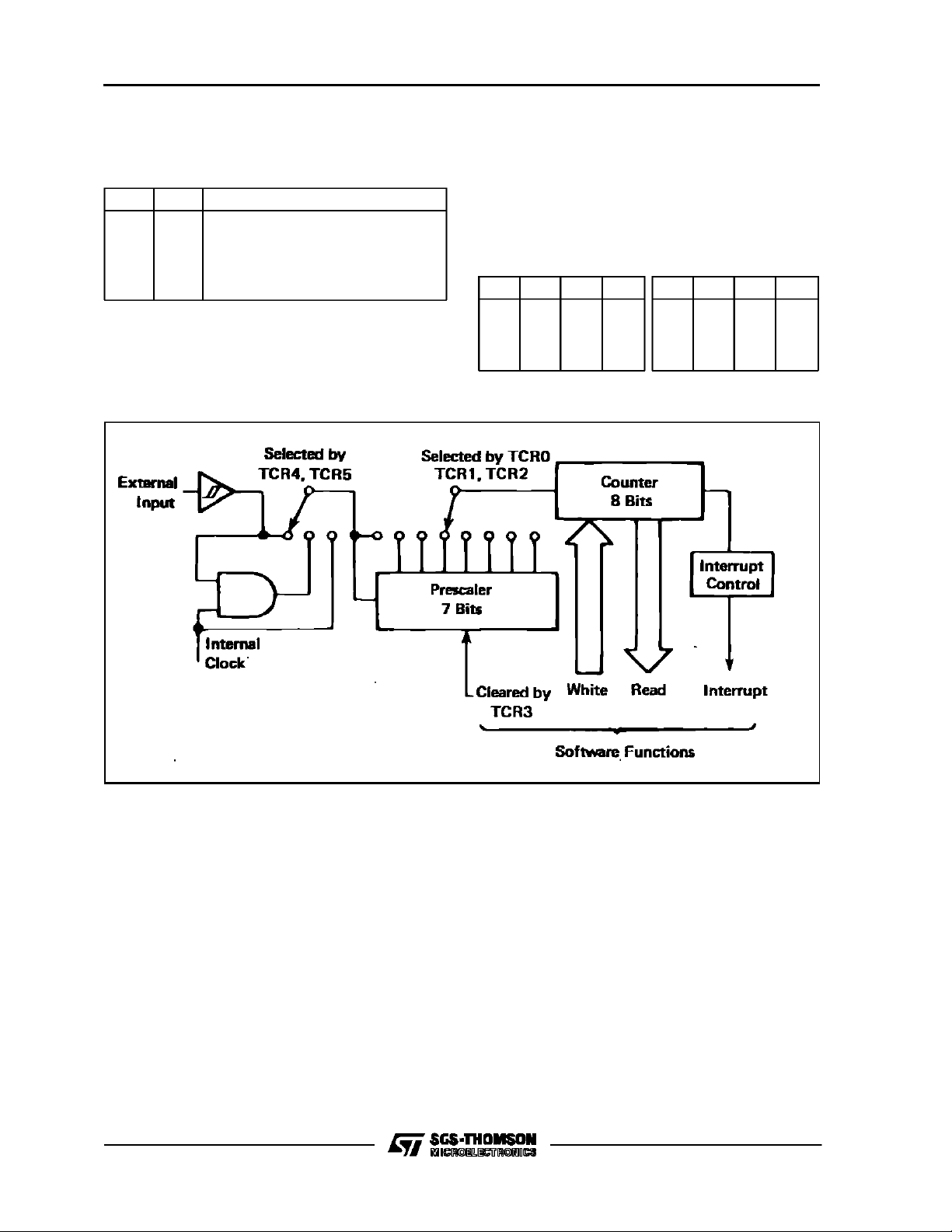
TIM ER
The timercircuitry for theEF6805U3is shown infigure 10. The timer contains a single 8-bit software
programmable counter with a 7-bit software selectable prescaler. The counter may be preset under
program control and decrements toward zero.
When the counterdecrements to zero, the timerinterrupt request bit, i.e., bit 7 of the timer control register(TCR),is set. Thenif the timer interrupt is not
masked, i.e.,bit 6 of the TCR and the I bit in the
conditioncoderegister arebothcleared, the processorreceivesaninterrupt.Aftercompletionofthecurrentinstruction,the processor proceeds tostore the
appropriate registers on the stack,and thenfetches
the timer interrupt vector from locations $FF8 and
$FF9 inorder to begin servicing the interrupt.
Thecountercontinuestocountafterit reaches zero,
allowing the softwaretodetermine the number ofinternalor external input clocks since the timer interrupt request bit was set.The counter may be read
at any time by the processor without disturbing the
count. The contents of the counter become stable
priortothereadportionofacycleanddonotchange
during the read. The timer interrupt request bit remains setuntil cleared by the software. If awrite occursbeforethe timerinterrup issericed, theinterrupt
is lost.TCR7 may also be used as a scanned status
bitin a non-interrupt mode of operation (TCR6 = 1).
The prescaler is a 7-bit divider which is usedto extend the maximum length of the timer. Bit 0, bit 1,
andbit 2 of theTCR areprogrammed to choosethe
appropriate prescaler outptu which is used as the
counter input. The processor cannot writ eijto or
read from the prescaler ; however, its contentsare
cleared to all zeros by the write operation into TCR
when bit 3 of thewritten data equals one, which allows for truncation-free counting.
The timerinput canbe configured for threedifferent
operating modes, plus a disable mode, depending
on the value writtento the TCR4 and TCR5 control
bits. For further information seefigure 9.
Timer Input Mode 1 - If TCR5 adn TCR4 are both
programmed to a zero, the inpt to thetimer is from
an internal clock and the external TIMER inputisdisabled.The internal clock mode canbe used for periodic interrupt generation, as well as a referene in
frequency and event measurement. The internal
clockis the instruction cycle clock.
Timer Input Mode 2 - With TCR5 = 0 and TCR4 =
1, theinternalclockandtheTIMERinputpinareANDed toform the timerinput signal. Thismodecanbe
usedtomeasure externalpulse widths.Theexternal
timer input pulse simply turns on the internal clock
for the duration of the pulse widths.
TimerInputMode3 - IfTCR5=1andTCR4=0,then
all inputs tothe timer are disabled.
Timer InputMode4-If TCR5= 1 and TCR4=1,the
internal clock input to the timer is disabled and the
TIMERinput pinbecomes theinput to thetimer.The
external TIMER pin can, in this mode, be used to
count external events as well as external frequencies for generating periodic interrupts.
TCR7 - TimerInterruptRequest Bit :
76543210
TCR7TCR6 TCR5 TCR4 TCR3 TCR2 TCR1 TCR0$009
* Write only (read as zero).
1 - Set when TDR goes to zero, or under programcontrol
0 - Clearedon external Reset,Power-On-Reset,or under ProgramControl.
TCR6 - Timer Interrupt Mask Bit :
1 - Timer Interrupt masked (disabled) Set on
external Reset, Power-On-Reset, or under
Program Control
0 - Clearedunder Program Control.
TCR5 - External or Internal ClockSource Bit:
1 - External Clock Source. Set on externalReset, Power-On-Reset, or under Program
Control
0 - Clearedunder Program Control.
TCR4 - External Enable Bit :
1 - Enable external TIMERpin.Set on external
Reset, Poxer-On-Reset, or under Program
8/31
EF6805U3
Control.
0 - Clearedunder Program Control.
TCR3 - Timer prescaler reset bit : Aread of TCR3
TCR5 TCR4 Result
0
0
1
1
0
Internal Clock to Timer
1
AND of Internal Clock and TIMER
Pin to Timer
0
Input to timer disabled.
1
TIMER Pin to Timer
always indicates a zero.
1 - Set on externalReset, Power-On-Reset or
under Program Control.
0 - Clearedunder Program Control
Figure 10 : Timer Block Diagram.
TCR2 , TCR1, and TCR0 - Prescaler address
bits :
1 - All set on external Reset, Power-On-Reset
or under Program Control.
0 - Cleared under Program Control.
Figure9 : Timer Control Register (TCR).
TCR2 TCR1 TCR0 Result
0
0
0
1
0
0
0
1
0
1
1
0
TCR2 TCR1 TCR0 Result
+1
+2
+4
+8
0
1
0
1
1
1
1
1
0
1
0
1
+16
+32
+64
+128
Notes : 1. Prescaler and8-bit counter are clockedon thefailingedgeof the internal clock (AS)or external input.
SELF-CHECK - The self-check capability of the
EF6805U3 MCU provides an internal check to determineifthepart isfunctional.Connect theMCU as
shownin figure 11 and monitorthe output of Port C
bit 3 for an oscillation of approximately 7Hz. A 10volt level(through a 10k resistor) on thetimer input,
pin 8 and pressing then releasing the RESET button, energizes the ROM-based self-check feature.
The self-check program exercices the RAM, ROM,
TIMER, interrupts, and I/O ports.
Several of the self-checksubroutines can be called
by a user program with a JSR or BSR instruction.
TheyaretheRAM,ROM.Thetimerroutinemayalso
be called ifthe timer input is the internal2 clock.
2. Counter is written toduring dat strobe(DS) and counts down continuously.
To call those subroutines in customer application,
please contact your local SGS-THOMSON Microelectronics sales office in order to obtain the
complete description of the self-check program and
the entrance/exit conditions.
RAMSELF-CHECKSUBROUTINE- TheRAM selfcheckis calledat location $F84 andreturnswiththe
Z bit clear if any error is detected ; otherwise the Z
bit is set.The RAM test causes each byte to count
from0 upto 0 again with a check after each count.
The RAM test must be called with the stack pointer
at $07F and A= 0. Whenrun,thetest checks every
RAM cell except for $07F and $07E which are assumedto containthe return address.
9/31

EF6805U3
The A and X registersandallRAM locations except
$07F and $07E are modified.
ROM CHECKSUM SUBROUTINE - The ROM selfcheck is called at location $F95. The A register
should be cleared before calling the routine. If any
error is detected, it returns with the Z bit cleared ;
Figure 11 : Self-check Connections.
otherwise Z= 1, X = 0 on return,and A is zero if the
testpasses. RAM location $040to $043 is overwritten.The checksumisthecomplement of theexecutionOR ofthe contents of the user ROM.
* This connection depends on clock oscillator user selectable
mask option. Use jumper if the RC mask option is selected.
LED MEANINGS
PC0 PC1 PC2 PC3
1
0
1
0
Bad I/O
0
0
1
0
Bad Timer
1
1
0
0
Bad RAM
0
1
0
0
Bad ROM
0
0
0
0
Bad Interrupts or RequestFlag
All Flashing Good Device
10/31
Remarks
(1 : LED ON ; 0 : LED OFF)

EF6805U3
TIMER SELF-CHECK SUBROUTINE - The timer
self-checkiscalledatlocation $F6Dandreturnswith
the Z bit cleared if any error was found ; otherwise
Z=1.
In order to work correctly as a user subroutine, the
internal 2 clock mustbe the clockingsourceandinterrupts must be disabled. Also,on exit, the clock is
runningandtheinterruptmaskisnotsetsothecaller
mustprotect from interrupts if necessary.
The Aand X register contentsare lost.This routine
sets the prescaler for divide-by-128 and the timer
data register iscleared. TheXregister isconfigured
to count down the same as thetimer data register.
The tworegisters are then compared every128 cycles until they both count down to zero. Any mismatchduringthe countdownisconsideredasanerror. The A and X registers are cleared on exitfrom
the routine.
Figure 12 : TypicalReset SchmittTrigger Hysteresis.
RESET
The MCU can be reset three ways: by initial powerup, by the external reset input (RESET) and by an
optional internal low-voltage detect circuit. The RESETinput consistsmainlyofa Schmitttriggerwhich
senses the RESET line logic level. A typicalreset
Schmitt trigger hysteresis curve is shown in figure
12. The Schmitt trigger provides an internal reset
voltageifit sensesa logicalzeroontheRESET pin.
Power-On Reset (POR) - Aninternal reset is generated upon powerup that allows the internal clock
generator to stabilize. A delay of t
milliseconds
RHL
is required before allowing the RESET input to go
high. Refer to the power and reset timing diagram
of figure 13. Connecting a capacitor to the RESET
input (as illustrated in figure 14) typically provides
sufficient delay.During powerup,the Schmitt trigger
switcheson (removes reset) when RESET risesto
V
.
IRES+
Figure 13 : Power and Reset Timing.
11/31

EF6805U3
Figure 14 : RESET Configuration.
ExternalReset Input - TheMCU willbereset if a logicalzero is applied to the RESETinput fora period
longerthanone machinecycle(t
of reset, the Schmitttrigger switchesoffat V
).Underthistype
cyc
IRES-
to
provide an internal reset voltage.
Low-Voltage Inhibit (LVI)-The optional low-voltage
detectioncircuitcausesa reset of theMCUif the power supply voltage falls below a certain level (V
LVI
Theonly requirement isthatVCCremainsat orbelow
the V
threshold for one t
LVI
minimum. In typical
cyc
applications, the VCCbus filter capacitor will eliminate negative-going voltage glitches of less than
onet
. The output from thelow-voltage detectoris
cyc
connecteddirectly totheinternalresetcircuitry.Italso forces the RESET pin low via a strongdischarge
devicethrough a resistor.The internal reset will be
removed once thepowersupply voltagerisesabove
a recoverylevel (V
), at which time a normal po-
LVR
wer-on-reset occurs.
INTERNA L C LO C K GENERATOR O PTIO N S
Theinternalclockgeneratorcircuitisdesignedtorequirea minimum of externalcomponents. Acrystal,
a resistor, a jumper wire, or an external signal may
be usedtogenerate a systemclock withvariousstability/costtradeoffs. Theoscillatorfrequency isinternallydivided by four to produce the internal system
clocks.A manufacturing mask option is usedto select crystalor resistor operation.
The differentconnection methods are shown in figure 15. Crystal specifications and suggested PC
board layouts are given in figure 16. A resistor selectiongraph is given in figure 17.
The crystal oscillator start-up time is a function of
manyvariables: crystalparameters (especially RS),
oscillator load capacitances, IC parameters, ambient temperature, and supply voltage. To ensure
).
rapid oscillator start up, neither the crystal characteristics nor the load capacitances should exceed
recommendations.
When utilizing the on-board oscillator, the MCU
shouldremain ina resetcondition (reset pin voltage
belowV
) untilthe oscillator hasstabilizedat its
IRES+
operating frequency. Several factorsareinvolved in
calculating the external reset capacitor required to
satisfythis condition ; the oscillatorstart-up voltage,
theoscillatorstabilization time,theminimumV
and the reset charging current specification.
OnceVCCminimum isreached,the externalRESET
capacitor willbeginto chargeataratedependent on
thecapacitorvalue.Thechargingcurrent issupplied
from VCCthrougha large resistor, so itappears almost like a constant current source until the reset
voltage rises above V
. Therefore, the RESET
IRES+
pin will charge at approximately :
(V
IRES+
).C
ext=IRES.tRHL
Assumingthe external capacitor is initially discharged.
IRES+
,
12/31

Figure 15 : Clock Generator Options.
EF6805U3
Note : The recommended CL value with a 4.0 MHz crystal is 27pF, maximum, including system distributed capacitance. There is an internal capacitance of approximately 25pF on the XTAL pin. For crystal frequencies other than 4MHz, the total capacitance on each pin
should be scaled as the inverse of the frquency ratio. For example, with a 2MHz crystal, use approximately 50pF on EXTAL and approximately 25pF on XTAL. The exact value depends on the Motional-Arm parameters of the crystal used.
Figure 16 : CrystalMotional ARM parameters and Suggested PC Board layout.
13/31

EF6805U3
Figure 17 : TypicalFrequency Selection for resistor(oscillator option).
INTERRU PT S
The microcomputers can be interrupted four differentways: through the external interrupt (INT)input
pin, the internal timerinterrupt request, theexternal
portDbit6(INT2) inputpin,orthesoftwareinterrupt
instruction (SWI). When any interrupt occurs : the
current instruction (including SWI) is completed,
processing is suspended, the present CPU state is
pushed onto the stack, the interrupt bit (I) in the
condition code registeris set,the address of the interrupt routine is obtained from the appropriate interrupt vector address, and the interrupt routine is
executed. Stacking the CPU register, setting the I
bit, and vectorfetching require a total of 11 t
cyc
periodsfor completion. A flowchart of the interrupt sequence isshown in figure 18. Theinterrupt service
routine must end with a return from interrupt (RTI)
instructionwhichallowsthe MCUtoresume processing of the program prior to the interrupt (by unstacking the previous CPU state). Unlike RESET,
hardware interrupts do not cause the current instructionexecution to be halted, but are considered
pending until the current instruction execution is
complete.
When the current instruction is complete, the processor checks all pending hardware interrupts and
if unmasked, proceeds with interrupt processing ;
otherwise thenextinstruction is fetchedand executed.Note thatmasked interrupts arelatchedforlater
interrupt service.
If both anexternal interrupt and atimerinterrupt are
pending at the end of an instruction execution, the
external interrupt is serviced first. The SWI is executed as any other instruction.
14/31

Figure 18 : RESET and interrupt Processing Flowchard.
EF6805U3
NOTE
ThetimerandINT2interrupts sharethesamevector
address. The interrupt routine must determine the
sourceby examiningtheinterrupt request bits(TCR
b7 and MR b7). Both TCR b7 and MR b7 can only
be written to zero by software.
The external interrupt, INT and INT2, are synchronizedand then latched onthe falling edge of the input signal. The INT2 interrupt has an interrupt requestbit (bit 7) and a maskbit (bit 6) located in the
miscellaneous register (MR). The INT2 interrupt is
inhibited when the mask bit is set. The INT2 is alwaysreadasadigital inputon portD.The INT2 and
timerinterruprequests bits, if set,causetheMCUto
process an interruptwhen the conditioncode I bitis
clear.
A sinuoidalinputsignal (f
maximum)canbe used
INT
to generate an external interruptfor use as a zerocrossingdetector.This allows applications such as
servicingtime-of-day routines and engaging/disengagingac powercontrol devices. Off-chipfull wave
rectificationprovidesaninterrupt at everyzerocrossingofthe acsignal andthereby provides a 2f clock.
Seefigure 19.
NOTE
The INT (pin 3) is internally biasedat approximately
2.2Vdue to the internalzero-crossing detection.
15/31

EF6805U3
A softwareinterrupt (SWI) is an executable instruction whichis executed regardless of thestate of the
I bit in the condition code register. SWIs areusually
Figure 19 : TypicalInterrupt Circuits.
used as break-points for debugging or a system
calls.
INPUT/OUTPUT CIRCUITRY
There are 32 input/output pins. TheINT pin may be
polledwith branchinstructions toprovide anadditional input pin. All pins on ports A,B, and C are programmable as either inputs or outputs under softwarecontrol of the corresponding data direction register (DDR). See below I/O port control registers
configuration. The port I/O programming is accomplished by writing the corresponding bit in the
portDDR to a logic one foroutputor a logiczerofor
input.On reset allthe DDRs are initialized to a logic
zero state,placing the portsin the input mode. The
portoutput registers are not initialized on reset and
should be initializedbysoftwarebeforechanging the
DDRs from input to output. A read operation on a
portprogrammed asanoutput willreadthecontents
of the output latch regardless of the logic levels at
the output pin, due to outputloading. Referto figure
20.
PORT DATA REGISTER
70
PortA Addr= $000
PortB Addr= $001
PortC Addr = $002
PortD Addr = $003
PORT DAT A DIREC TIO N REGISTER (DDR )
70
(1) Writeonly ; readsas all“1s”
(2) 1 = Output.0 =input Clearedto 0 by Reset
(3) Port A Addr = $004
PortB Addr =$005
PortC Addr= $006
16/31

Figure 20: Typical Port I/O Circuitry.
EF6805U3
Data
Direction
Regis t er
Bit
1
1
0
Latche d
Output
Data
Bit
0
1
X
Output
State
0
1
High-Z**
Input
to
MCU
0
1
Pin
All input/output lines areTTL compatible as both inputsand outputs. PortAlinesareCMOScompatible
asoutputs(maskoption)whileport B,C,andDlines
areCMOScompatible asinputs.PortD linesareinput only ; thus, there is no corresponding DDR.
When programmed as outputs,port B is capable of
sinking10 milliamperes and sourcing 1milliampere
on each pin.
The address map (figure 6) gives the addresses
of data registers and data direction registers.
Figure 21 provides some examples of port
connections.
CAUTION
The corresponding DDRs for ports A, B, and C are
write-only registers (registers at$004, $005, $006).
* DDRis a write-only register and reads as all ”1s”.
** Ports B and C are three-state ports.
Port A has optional internal pull-up devices to provide CMOS data
drive capability. See Electrical Characteristic tables for complete information.
A read operation on these registers is undefined.
Since BSET and BCLR are read-modify-write in
function, they cannotbeusedto setor clearasingle
DDRbit (all ”unaffected” bitswould be set). It is recommended thatall DDR bits in a port be writtenusing a single-store instruction.
The latched output data bit(see figure 20) must alwaysbe written.Therefore, any writeto aportwrites
all of its data bits even though the portDDR isset
to input. This may be used to initialize the data register and avoid undefined outputs ; however, care
mustbeexercised whenusing read-modify-write instructions, since the data read corresponds to the
pin level if the DDR is an input (zero) and corresponds to the latched output data when the DDR is
anoutput (one).
17/31

EF6805U3
Figure 21: Typical Port Connections.
18/31

EF6805U3
SOFTWARE
BIT MANIPULATION
The EF6805U3 MCU has the abilityto set or clear
any single random access memory or input/output
bit (except the data direction register, see Caution
below), with a singleinstruction (BSET, BCLR).Any
bit in page zero including ROM, except the DDRs,
can be tested, using the BRSET and BRCLR instructions, and the program branches as a resultof
itsstate.The carrybit equals the value ofthe bit referenced by BRSET or BRCLR. A rotate instruction
may then be usedto accumulate serial input data in
a RAM location or register. The capability to work
withany bit in RAM,ROM, or I/O allows the user to
haveindividual flags in RAMorto handle I/O bitsas
controllines.
The codingexample in figure 21 illustrates the usefulness of thebitmanipulation andtest instructions.
Figure 21 : Bit Manipulation Example.
AssumethattheMCUis tocommunicatewithanexternal serial device.
The external device has a data readysignal, a data
outputline, and a clock line to clockdata one bit at
a time. LSB first, out of the device.The MCU waits
until the data is ready, clocks the external device,
picksup the data in the carryflag (C bit), clears the
clock line, and finally accumulates thedata bit in a
RAM location.
Caution
The corresponding DDRs for ports A, B, and C
are write-only registers (registers at $004, $005,
and $006). A read operation on these registers
is undefined. Since BSET and BCLR are readmodify-write functions, they cannot be used to
set or clear a DDR bit (all ”unaffected” bits would
be set). It is recommended that all DDR bits in a
port be written using a single-store instruction.
AD D RESSING MO DES
The EF6805P2 MCU has 10 addressing modes
which are explained briefly in the following paragraphs.For additional details and graphical illustrations,refer to the6805 Family User’s Manual.
The term ”effective address” (EA) is used in describing the address modes. EA is defined as the address from which the argument for an instruction is
fetched or stored.
IMMEDIATE - In the immediate addressing mode,
theoperand iscontainedin thebyteimmediatelyfollowing the opcode. The immediate addressing
mode is used to access constants which do not
change during program execution (e.g;, a constant
used to initializea loopcounter).
DIRECT - In the direct addressing mode,the effectiveaddress oftheargument is contained in asingle
bytefollowing the opcode byte.Directaddresing al-
lows the user to directly address the lowest 256
bytes in memory with a single 2-byte instruction.
Thisincludestheon-chipRAM andI/Oregisters and
128 bytes of ROM. Direct addressing is an effective
use of both memory and time.
EXTENDED -Intheextendedaddressingmode,the
effectiveaddressoftheargumentiscontained in the
two bytes following the opcode. Instructions using
extended addressing arecapable of referencing arguments anywhere in memory with a single 3-byte
instruction.WhenusingtheMotorolaassembler,the
programmerneed notspecifywhetheraninstruction
usesdirect or extendedaddressing. Theassembler
automatically selects the shortest for of the instruction.
RELATIVE - The relative addressing mode is only
used in branch instructions. In relative addressing,
thecontentsofthe8-bitsignedbytefollowing theopcode(the offset)isaddedtothe PCif and only if the
19/31

EF6805U3
branch condition is true. Otherwise, control proceeds to the next instruction. The span of relative
addressing is from- 126 to + 129 from the opcode
address.Theprogrammer neednotworryaboutcalculatingthe correct offset when using the Motorola
assemblersince it calculates the proper offset and
checksto seeif it is within the span of thebranch.
INDEXED, NO OFFSET - In the indexed, no offset
addressing mode,the effectiveaddressof theargument is contained in the 8-bit index register. Thus,
this addressing mode canaccess the first256 memorylocations. These instructionsareonlyonebyte
long. This mode is often used to move a pointer
through a tableor toholdthe address of afrequently
referenced RAM or I/Olocation.
INDEXED,8-BIT OFFSET- In theindexed,8-bitoffset addressing mode, the effective address is the
sum of the contents of the unsigned 8-bit index registerand the unsigned byte following the opcode.
This addressing mode is useful in selecting the kth
element in ann element table. With this 2-byte instruction,k would typically be in X with the address
of the beginning of the table in the instruction. As
such,tablesmaybeginanywhere withinthefirst256
addressablelocationsandcouldextendasfaras location510($1FEis thelastlocationatwhichtheinstructionmay begin).
INDEXED, 16-BIT OFFSET - In the indexed, 16-bit
offsetaddressing mode,the effectiveaddress is the
sum of the contents of the unsigned 8-bit index registerand the two unsignedbytes following the opcode.Thisaddressing mode can be used in a manner similar to indexed, 8-bit offset, except that this
3-byte instruction allows tables to be anywhere in
memory. As with direct and extended addressing,
the Motorola assembler determines the shortest
form of indexed addressing.
BIT SET/CLEAR - In the bit set/clear addressing
mode,the bit to be set or cleared is part of the opcode, and the byte following the opcode specifies
thedirect address of the byte in whichthe specified
bitis to be set or cleared. Thus,any read/write bit in
thefirst256 locations ofmemory, including I/O, can
beselectivelyset or cleared witha single 2-byteinstruction.
Caution
The corresponding DDRs for ports A, B, and C
are write-only registers (registers at $004, $005,
and $006). A read operation on these registers
is undefined. Since BSET and BCLR are readmodify-write functions, they cannot be used to
set or clear a DDR bit (all ”unaffected” bits would
be set). It is recommended that all DDR bits in a
port be written using a single-store instruction.
BITTEST AND BRANCH - The bit test and branch
addressing mode is a combination of directaddressing and relative addressing. The bit and condition
(setor clear) whichis to be testedis includedin the
opcode, and the address of the byte to be tested is
in the single byte immediately following the opcode
byte. The signed relative 8-bit offset is in the third
byteandisaddedtothevalueofthe PCifthebranch
conditionistrue.Thissingle3-byte instructionallows
theprogram tobranchbased on thecondition ofany
readablebitinthe first256locationsofmemory.The
spanof branching isfrom- 125to+130fromtheopcode address. The state of the tested bit is also
transferred to thecarry bit of the conditioncode register.
Caution
The corresponding DDRs for ports A, B, and C
are write-only registers (registers at $004, $005,
and $006). A read operation on these registers
is undefined. Since BSET and BCLR are readmodify-write functions, they cannot be used to
set or clear a DDR bit (all ”unaffected” bits would
be set). It is recommended that all DDR bits in a
port be written using a single-store instruction.
INHERENT - In the inherent addressing mode, all
theinformationnecessary to executetheinstruction
is contained in the opcode. Operations specifying
only the index register or accumulator, as well as
controlinstruction with no other arguments, are included inthismode. Theseinstructions areone byte
long.
INSTRUCTION SET
The EF6805U3 MCU has a setof 59 basic instructions,whichwhen combined with the10addressing
modes produce 207 usable opcodes. They can be
divided into five different types : register/memory,
read-modify-write, branch, bit manipulation, and
control. The following paragraphs briefly explain
eachtype.Alltheinstructionswithin agiven typeare
presented in individual tables.
REGISTER/MEMORY INSTRUCTIONS - Most of
these instructions use two operands. One operand
is either the accumulator or the index register. The
other operand is obtained from memory using one
of the addressing modes. The jump unconditional
(JMP) and jump to subroutine (JSR) instructions
haveno register operands. Refer to table 1.
READ-MODIFY-WRITE MODIFICATIONS-These
instructions read a memory location or a register,
20/31

EF6805U3
modifyortestitscontents,andwrite themodifiedvalue back to memory or to the register. The test for
negative or zero (TST) instruction is included in
read-modify-write instructions through it does not
perform thewrite. Rfer to table 2.
Caution
The corresponding DDRs for ports A, B, and C
are write-only registers (registers at $004, $005,
and $006). A read operation on these registers
is undefined. Since BSET and BCLR are readmodify-write functions, they cannot be used to
set or clear a DDR bit (all ”unaffected” bits would
be set). It is recommended that all DDR bits in a
port be written using a single-store instruction.
BRANCH INSTRUCTIONS - The branch instructionscausea branch from the program when a certain condition is met. Refer to table 3.
BITMANIPULATIONINSTRUCTIONS-Theseinstructionsareused on any bit in the first256bytes of
thememory. Onegroup eithersets or clears.The other group performsthe bit test branch operations.
Refer to table 4.
Caution
The corresponding DDRs for ports A, B, and C
are write-only registers (registers at $004, $005,
and $006). A read operation on these registers
is undefined. Since BSET and BCLR are readmodify-write functions, they cannot be used to
set or clear a DDR bit (all ”unaffected” bits would
be set). It is recommended that all DDR bits in a
port be written using a single-store instruction.
CONTROL INSTRUCTIONS - The controlinstructions control the MCU operations during program
execution. Refer to table 5.
ALPHABETICAL LISTING - The complete instructionset is given in alphabetical order in table 6.
OPCODEMAP SUMMARY - Table 7 is an opcode
map for the instructions used on the MCU.
21/31

EF6805U3
Table 1 : Register/Memory Instructions.
22/31

Table 2 : Read-Modify-Write Instructions.
EF6805U3
23/31

EF6805U3
Table 3 : Branch Instructions.
Relative Addressing Mode
Function Mnemonic
Branch Always BRA 20 2 4
Branch Never BRN 21 2 4
Branch IFF Higher BHI 22 2 4
Branch IFF Lower or Same BLS 23 2 4
Branch IFF Carry Clear BCC 24 2 4
(branch IFF higher or same) (BHS) 24 2 4
Branch IFF Carry Set BCS 25 2 4
(branch IFF lower) (BLO) 25 2 4
Branch IFF Not Equal BNE 26 2 4
Branch IFF Equal BEQ 27 2 4
Branch IFF Half Carry Clear BHCC 28 2 4
Branch IFF Half Carry Set BHCS 29 2 4
Branch IFF Plus BPL 2A 2 4
Branch IFF Minus BMI 2B 2 4
Branch IFF interrupt mask bit is clear. BMC 2C 2 4
Branch IFF interrupt mask bit is set. BMS 2D 2 4
Branch IFF interrupt line is low. BIL 2E 2 4
Branch IFF interrupt line is high. BIH 2F 2 4
Branch to Subroutine BSR AD 2 8
Op
Code
#
Bytes
#
Cycles
Table 4 : Bit Manipulation Instructions.
Addressing Mo d es
Function Mnemonic
Branch IFF Bit n is set BRSET n (n = 0… 7) 2 • n3 10
Branch IFF Bit n is clear BRCLR n (n = 0… 7)
Set Bit n BSET n (n = 0… 7)
Clear Bit n BCLR n (n =0… 7)
Bit Set/clear Bit T est an d Branch
Op
Code#Bytes#CyclesOpCode#Bytes#Cycles
01 + 2 • n 310
10 + 2 • n 27
11 + 2 • n 27
24/31

EF6805U3
Table 5 : Control Instructions.
Inherent
Function Mnemonic
Op
Code
Transfer A to X TAX 97 1 2
Transfer X to A TXA 9F 1 2
Set Carry Bit SEC 99 1 2
Clear Carry Bit CLC 98 1 2
Set Interrupt Mask Bit SEI 9B 1 2
Clear Interrupt Mask Bit CLI 9A 1 2
Software Interrupt SWI 83 1 11
Return from Subroutine RTS 81 1 6
Return from Interrupt RTI 80 1 9
Reset Stack Pointer RSP 9C 1 2
No-operation NOP 9D 1 2
Table6 : Instruction Set.
Addressing Modes Condition Code
Mnem Inherent Immediate Direct Extended Relative
ADC X X X X X X ∧ ● ∧∧∧
ADD X X X X X X ∧ ● ∧∧∧
AND X X X X X X ●●∧∧●
ASL X X X X ●●∧∧∧
ASR X X X X ●● ∧∧∧
BCC X ●●●●●
BCLR X ●●●●●
BCS X ●●●●●
BEQ X ●●●●●
BHCC X ●●●●●
BHCS X ●●●●●
BHI X ●●●●●
BHS X ●●●●●
BIH X ●●●●●
BIL X ●●●●●
BIT X X X X X X ●●∧∧●
BLO X ●●●●●
BLS X ●●●●●
BMC X ●●●●●
BMI X ●●●●●
BMS X ●●●●●
BNE X ●●●●●
BPL X ●●●●●
BRA X ●●●●●
BRN X ●●●●●
BRCLR X ●●●● ∧
BRSET X ●●●●∧
BSET X ●●●●●
BSR X ●●●●●
CLL X ●●●● 0
Indexed
(no offset)
Indexed
(8 Bits)
Indexed
(16 Bits)
Bit
Set/Clear
Bit
Test &
Branch
#
Bytes
HINZC
Cycles
#
25/31

EF6805U3
Table6 : Instruction Set (continued).
Addressing Modes Condition Code
Mnem Inherent Immediate Direct Extended Relative
Indexed
(no offset)
Indexed
(8 Bits)
Indexed
(16 Bits)
Bit
Set/clear
CLI X ● 0 ●●●
CLR X X X X ●● 01●
CMP X X X X X X ●●∧∧∧
COM X X X X ●● ∧∧1
CPX X X X X X X ●●∧∧∧
DEC X X X X ●●∧∧●
EOR X X X X X X ●●∧∧●
INC X X X X ●●∧∧●
JMP X X X X X ●●●●●
JSR X X X X X ●●●●●
LDA XXX XXX ●●∧∧●
LDX XXX XXX ●●∧∧●
LSL X X X X ●●∧∧∧
LSR X X X X ●● 0 ∧∧
NEQ X X X X ●●∧∧∧
NOP X ●●●●●
ORA X X X X X X ●●∧∧●
ROL X X X X ●●∧∧∧
RSP X ●●●●●
RTI X ?????
RTS X ●●●●●
SBC XXX XXX ●●∧∧∧
SEC X ●●●● 1
SEI X ● 1 ●●●
STA XX XXX ●●∧∧●
STX XX XXX ●●∧∧●
SUB XXX XXX ●●∧∧∧
SWI X ● 1 ●●●
TAX X ●●●●●
TST X X X X ●● ∧∧●
TXA X ●●●●●
Condition Code Symbols :
H Half Carry (from bit3)
I Interrupt Mask
N Negative (sign bit)
Z
C
^ Test and Set if True, Cleared Otherwise
• Not Affected
Bit
Test &
Branch
HINZC
26/31

EF6805U3
HMOS 6805 FAMILY
Features EF 6 805P2 EF680 5P6 EF 6805R2 EF 6805R 3 EF68 05U2 EF 6805 U3
Technology HMOS HMOS HMOS HMOS HMOS HMOS
Number of Pins 28 28 40 40 40 40
On-chip RAM (bytes) 64 64 64 112 64 112
On-chip User ROM (bytes) 1100 1796 2048 3776 2048 3776
External Bus None None None None None None
Bidirectional I/O Lines 20 20 24 24 24 24
Unidirectional I/O Lines None None 6 Inputs 6 Inputs 8 Inputs 8 Inputs
Other I/O Features Timer Timer Timer, A/D Timer, A/D Timer Timer
External Interrupt Inputs 1 1 2 2 2 2
STOP and WAIT No No No No No No
27/31

EF6805U3
Table 7 : 6805 HMOS Family Opcode MAP.
28/31

PACKAGE MECHANICAL DATA
40 Pin Plastic Dual In Line Package (PDIP)
EF6805U3
Dim. mm inches
Min Typ Max Min Typ Max
A 2.2 4.8 0.086 0.189
A1 0.51 1.77 0.010 0.069
B 0.38 0.58 0.015 0.023
B1 0.97 1.52 0.055 0.065
C 0.2 0.3 0.008 0.009
D 50.30 52.221.980 20.56
D1------
E 16.3 0.641
E1 12.9 0.508
K1––––––
K2––––––
L 3.18 4.44 1.25 0.174
e1 2.54 0.10
Number of Pins
N40
44 Pin Plastic Quad Package (PLCC)
Dim. mm inches
Min Typ Max Min Typ Max
A 4.2 5.08 0.165 0.200
A1 0.64 0.020
A3 2.29 3.30 0.090 0.130
B 0.331 - ---B1 0.661 - ----
D 17.40 17.650.685 0.695
D1 16.51 16.660.650 0.656
D3 12.70 0.500
E 17.40 17.650.685 0.695
E1 16.51 16.660.650 0.656
E3 12.70 0.500
K1------
e 1.27 0.050
Number of Pins
N44
ND 11
29/31

EF6805U3
ORDERING INFORMATION
The information required when ordering a custom
MCU is listed below. The ROM program may be
transmitted toSGS-THOMSONonEPROM(s)oran
EFDOS/MDOS* disk file.
To initiate a ROM patternfor theMCU, it isnecessary to firstcontactyour local SGS-THOMSON representative or distributor.
EPROMs
One2716 or2732typeEPROMs, programmed with
the customer program (positive logic sense for ad-
XXX = Customer ID)
dress and data), may be submitted for pattern generation.
After the EPROM is marked, it should be placed in
conductive IC carriersand securely packed. Do not
use styrofoam.
VERIFICA TION MEDI A
All original pattern media (EPROMsor floppydisk)
arefiled for contractualpurposes and are not returned. A computer listing of the ROMcode willbe generatedand returned along withalistingverification
form. The listingshould be thoroughly checked and
the verification form completed, signed, and returned to SGS-THOMSON. The signed verification
formconstitutesthecontractualagreement for creation of thecustomermask. If desired, SGS-THOM-
SON will program on blank EPROM from the data
file used to create the custom mask and aid in the
verification process.
ROM VERIFICATION UNITS (RVUs)
Ten MCUs containing thecustomer’sROM pattern
will be sent for program verification. Theseunitswill
havebeen made usingthe custom mask but are for
the purposeof ROMverification only. Forexpediency theyare usuallyunmarked, packaged inceramic,
and tested only at room temperature and 5 volts.
TheseRVUs are included in the maskchange and
are not production parts. The RVUs are thus not
guaranteed by SGS THOMSON. Quality Assurance,and shouldbe discarded after verificationis
completed.
FLEXIB LE DIS KS
The diskmediasubmitted mustbesingle-sided, EFDOS/MDOS*compatiblefloppies.
The customer must write the binary file name and
company name on the disk with a felt-tip-pen. The
minimum EFDOS/MDOS* system files, as well as
the absolutebinaryobject file(Filename .LO type of
file)from the 6805 crossassembler,must be on the
disk.Anobjectfilemadefroma memorydump using
the ROLLOUTcommand isalso acceptable. Consider submitting a source listing as well as the followingfiles:filename.LX(DEVICE/EXORciser loadable format)and filename .SA (ASCII Source Code).
Thesefileswillofcoursebekeptconfidential andare
used1) tospeeduptheprocess in-house ifany problems arise, and 2) to speed up the user-to-factory
interface if the user finds any software errors and
needs assistance quickly from SGS-THOMSON
factoryrepresentatives.
EFDOSis SGS-THOMSON DiskOperating System
available on development systems such as DEVICE...
MDOS* is MOTOROLA’s Disk Operating System
available on development systems such as EXORciser...
* Requires prior factory approval.
Whenever ordering a custom MCU isrequired, please contactyourlocal SGS-THOMSON representative or
SGS-THOMSONdistributor and/or complete and send the attached ”MCU customerordering sheet” to your
localSGS-THOMSON Microelectronics representative.
30/31

ORDER C ODES
EF6805U3
EF6805U3 P V
Device
Package
Screen level
Oper. temp.
The tablebelow horizontally showsall available suffixcombinations for package, operating temperature and
screening level. Otherpossibilities on request.
Device Package Oper. Temp. Screenin g Lev el
C J P E FN L* V T Std D G/ B B/B
EF6805U3 X XXXXXX
Examples : EF6805U3P, EF6805U3FN, EF6805U3PV, EF6805U3FNV
Package : C : Ceramic DIL, J:Cerdip DIL, P:Plastic DIL, E:LCCC, FN : PLCC
Oper. temp. : L* : 0°Cto+70°C, V:–40°Cto+85°C,T:–40°C to + 105°C, *:may be omitted.
Screening level : Std : (no-end suffix), D:NFC 96883 level D,
EXORciser is a registered trademark of MOTOROLA Inc.
Information furnished is believed to be accurate and reliable. However, SGS-THOMSON Microelectronics assumes no
responsability for the consequences of use of such information nor for any infringement of patents or other rights of
third parties which may result from its use. No license is granted by implication or otherwise under any patent or
patent rights of SGS-THOMSON Microelectronics. Specifications mentioned in this publicationare subject to change
without notice. This publication supersedes and replacesall information previously supplied.
SGS-THOMSON Microelectronics products are not authorized for use as critical components in life support devices or
systems without the express writtenapproval of SGS-THOMSON Microelectronics.
1994 SGS-THOMSON Microelectronics - All rights reserved.
Purchase of I2C Components by SGS-THOMSON Microelectronics conveys a license under the Philips I2C Patent. Rights to use these
components in an I2C system is granted provided that the system conforms to the I2C Standard Specification as defined by Philips.
SGS-THOMSON Microelectronics Group of Companies
Australia- Brazil- France - Germany - HongKong - Italy - Japan - Korea - Malaysia- Malta- Morocco The Netherlands - Singapore - Spain
Sweden- Switzerland - Taiwan- Thailand - UnitedKingdom - U.S.A.
31/31
 Loading...