

®
DDR110-xxT7RL
ASD™
IPAD™ Computer
DOUBLE DATA RATE TERMINATION
NETWORK WITH DISABLE SWITCH
MAIN APPLICATION
DDR(doubledatarate)TerminationNetworkused
on.
Motherboard
■
Workstation
■
Server
■
Notebooks
■
DESCRIPTION
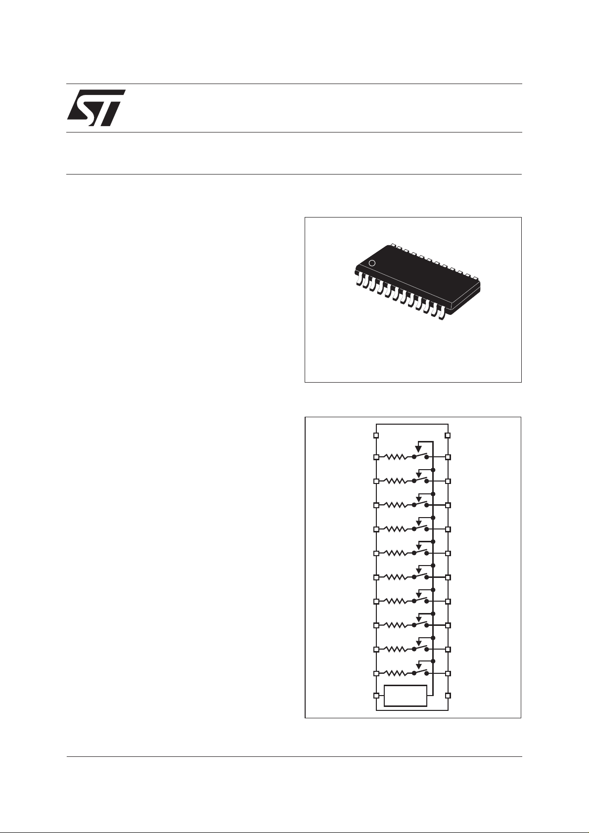
The DDR110 provides 10 bits resistor Network to
be used for SDR/DDR (double data rate) SDRAM
bus Termination.
This device has a series resistors (Rs) to reduce
signalreflectionnoise.Thiseliminatestheneedfor
external terminating resistors.
The DDR Termination Nerwork is enabled with the
output Enable pin (OE). When OE is HIGH Inputs
are connected to Outputs (A connected to B).
When OE is LOW every inputs are in High
impedance state (Hi - Z).
The DDR Termination Network is a bidirectional
device when the internal switch is ON. When the
switch is OFF, the device will block current in both
directions.
TM
This device is made using ST IPAD
(Integrated
Passive & Active devices) technology.
FEATURES AND BENEFITS
■
10 bits Termination Network.
■
Integrated Termination resistor (Rs)
■
Enable input TTL level compatible
■
Impedance matching ± 2% (A0-B0 / An-Bn)
■
Optimized Low Crosstalk for parallel
Termination to Vtt.
■
Optimized Low propagation delay
1
1
VSS
A0
A1
A2
A3
A4
A5
A6
A7
A8
A9
24
TSSOP24
Rs
Rs
Rs
Rs
Rs
Rs
Rs
Rs
Rs
Rs
12
VCC
B0
B1
B2
B3
B4
B5
B6
B7
B8
B9
24
May 2001 - Ed: 2
12
OE
GATE
CONTROL
NC
1/5

DDR110-xxT7RL
FUNCTION TABLE
OE B0 - B9 Function
High A0 - A9 Connect Termination
Low Hi - Z Disconnect Termination
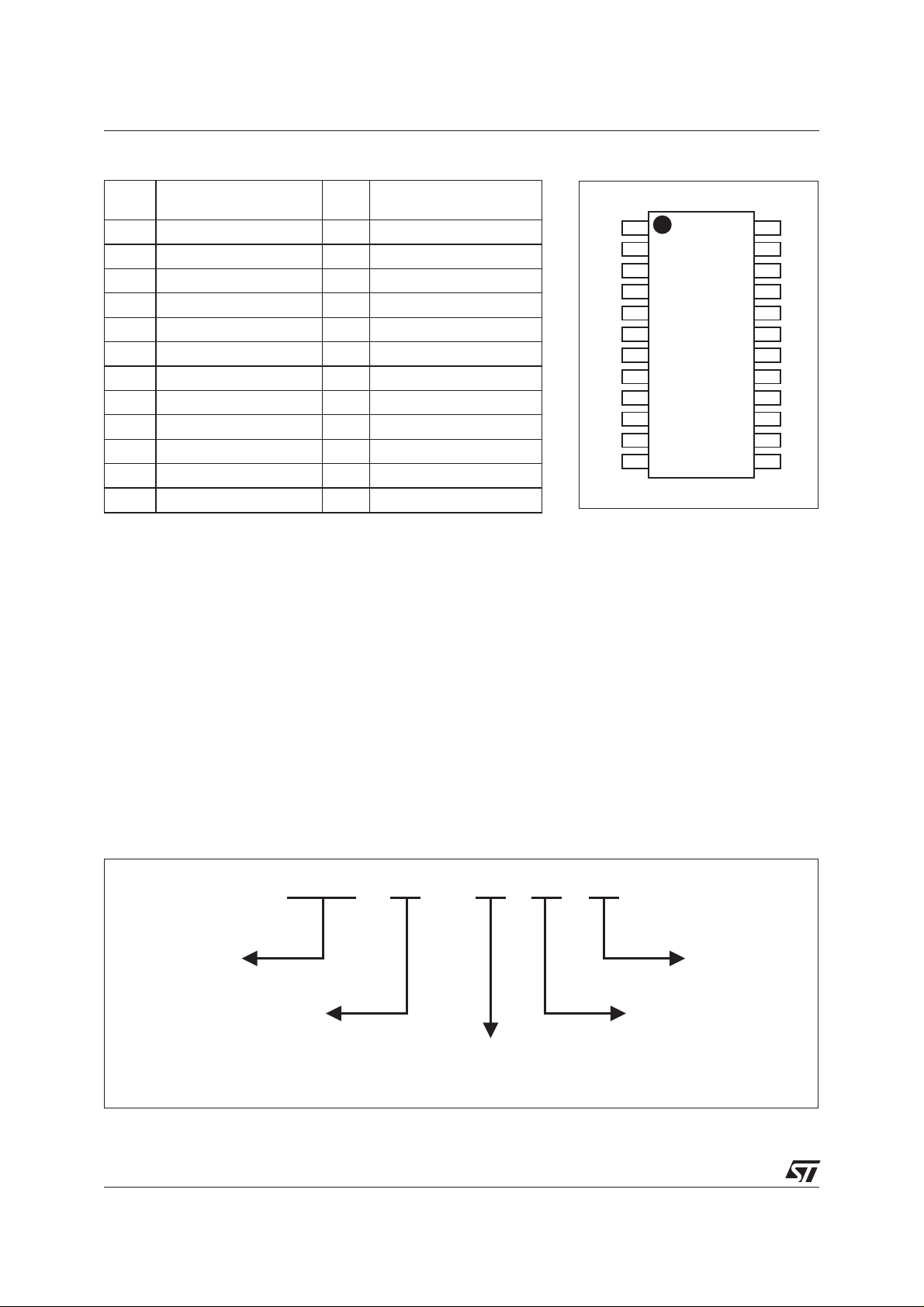
ABSOLUTE MAXIMUM RATINGS (Tamb = 25°C)
Value
Symbol Parameter Test Conditions
V
CC
V
Supply voltage range
Input voltage range DQ0/7, DM0,
IN
DQS0
V
TT
V
OE
I
IN
V
ESD
T
STG
Termination voltage
Termination Enable Voltage range
Continuous input current
ESD ratings (input / output YOE) HBM MIL STD 883C
Storage temperature
RECOMMENDED OPERATING CONDITIONS (Tamb = 25°C)
Symbol Parameter TestConditions
V
IN
Input voltage DQ0/7, DM0, DQS0 OE LOW
OE HIGH
V
IH
Output Enable (OE) HIGH voltage Guaranteed logic
HIGH level
V
IL
Output Enable (OE) LOW voltage Guaranteed logic
LOW level
V
CC
V
TT
(1) Opencollectoroutput with 10k pull-up resistor to 5V is recommended for typical OE signal.
Supply voltage
Termination voltage
UnitTambient = 25°C
Min. Typ. Max.
- 0.5 5 7 V
- 0.5 7 V
- 0.5 7 V
- 0.5 7 V
30 mA
2kV
- 65 150 °C
Value
Min. Typ. Max.
0
0
25
+ 3.3
+ 2.5
(1)
0.8 V
4.5 5 5.5 V
1.25 V
Unit
V
V
2/5
®

DDR110-xxT7RL
ELECTRICAL CHARACTERISTICS (Tamb = 25°C - Vcc = 5V)
Symbol Parameter Test conditions
R
ON
Switch ON Resistance VTT= 1.25V, VIN= 0V,OE=+5V
DDR110-27
DDR110-56
I
OFF
INPUT Leakage
INPUT = + 3.3V, OE = 0V
current Switch OFF
C
OFF
OFF-state capacitance VIN= 0V, 1MHz, 30mV
OE=0V
APPLICATION SCHEMATICS
DDR 184-pin DIMM slot
System
Controller
DDR Address
Chipset
DDR Control
Value
Min. Typ. Max.
22
45
,
RMS
5V
Enable
DDR 184-pin DIMM slot
SDR 168-pin DIMM slot
SDR 168-pin DIMM slot
10 bits
Unit
27
56
32
67
Ω
Ω
1µA
6pF
VTT
DDR
110
DDR
110
DQ7
DQ6
DM0
DQ5
DQ4
DQ3
DQ2
DQS0
DQ1
DQ0
GND
OE
(North Bridge)
OE
ENABLE HIGH
ENABLE HIGH
VCC
DDR Data / Strobe
V IslandTT
Decoupling
Capacitor
to GND Plane
NC
10 bits
10 bits
DDR
110
DDR
110
®
3/5
DDR110-xxT7RL
PIN ASSIGNEMENT
Pin #
Assignement for DDR
Termination
1 V
2 A0 23 B0
3 A1 22 B1
4 A2 21 B2
5 A3 20 B3
6 A4 19 B4
7 A5 18 B5
8 A6 17 B6
9 A7 16 B7
10 A8 15 B8
11 A9 14 B9
12 Termination enable HIGH 13 NotConnected
= GND 24 V
SS
Pin #
Assignement for DDR
Termination
CC
10
11
12
1
2
3
4
5
6
7
8
9
24
23
22
21
20
19
18
17
16
15
14
13
OTHER INFORMATION
Double Data Rate
Single switch
10-BIT Wide
4/5
DDR1 10 - 27 T7 RL
Rs value in
27 , 56
ΩΩ
Ω
Tape & Reel
Package code
T7:TSSOP24
®
PACKAGE MECHANICAL DATA
TSSOP-24
AA2
A1
b
D
24
1
e
13
E
12
DDR110-xxT7RL
DIMENSIONS
REF.
E1
k
L
L1
A 1.200 0.047
A1 0.050 0.150 0.002 0.006
c
A2 0.800 1.000 1.050 0.031 0.039 0.041
b 0.190 0.300 0.007 0.012
c 0.090 0.200 0.004 0.008
D 7.700 7.800 7.900 0.303 0.307 0.311
E 6.400 0.252
E1 4.300 4.400 4.500 0.169 0.173 0.177
e 0.65 0.026
k0°8°0°8°
L 0.450 0.600 0.750 0.017 0.024 0.029
L1 1.000 0.039
Millimeters Inches
Min. Typ. Max. Min. Typ. Max.
FOOTPRINT
0.65mm
6.8mm 4.4mm
0.30mm
8.00mm
Type Marking Package Weight Base qty Deliverymode
DDR110-27T7RL DDR110-27 TSSOP-24 0.088 g 2500 Tape & Reel
DDR110-56T7RL DDR110-56 TSSOP-24 0.088 g 2500 Tape & Reel
■
Epoxy meets UL94 - V0 standard
Informationfurnished is believedto be accurateand reliable. However,STMicroelectronics assumes noresponsibility for theconsequences of
useof such informationnor for anyinfringement of patentsor other rightsof third partieswhich may resultfrom its use.No license isgranted by
implication or otherwise under any patent or patent rights of STMicroelectronics. Specifications mentioned in this publication are subject to
change without notice. This publication supersedes and replaces all information previously supplied.
STMicroelectronics products are not authorized for use as critical components in life support devices or systems without express written approval of STMicroelectronics.
The ST logo is a registered trademark of STMicroelectronics
© 2001 STMicroelectronics - Printed in Italy - All rights reserved.
STMicroelectronics GROUP OF COMPANIES
Australia - Brazil - China - Finland - France - Germany - Hong Kong - India - Italy - Japan - Malaysia
Malta - Morocco - Singapore - Spain - Sweden - Switzerland - United Kingdom - U.S.A.
http://www.st.com
®
5/5
 Loading...