

FEATURES
V
:32V/34V/40VVERSIONS
BO
LOW BREAKOVERCURRENT
DB3 /DB4 / DC34
TRIGGER DIODES
DESCRIPTION
High reli a bility glas s passiva t i on insurin g
parameter stability and p rot ection aga inst
junction contamination.
ABSOLUTE RATINGS (limiting values)
Symbol Parameter Value Unit
P Power dissipation onprinted circuit
(L = 10 mm)
I
TRM
Tstg
Tj
Repetitive peak on-state current tp =20µs
Storageandoperatingjunction temperaturerange
Ta = 65 °C 150 mW
F= 100 Hz
DO 35
(Glass)
2A
-40to+125
-40to+125
°C
°C
THERMAL RESISTANCES
Symbol Parameter Value Unit
R
th (j-a)
R
th (j-l)
April 1995
Junction to ambient 400 °C/W
Junction-leads 150 °C/W
1/4
DB3 / DB4 / DC34
ELECTRICALCHARACTERISTICS (Tj = 25°C)
Symbol Parameter Test Conditions Value Unit
DB3 DC34 DB4
V
BO
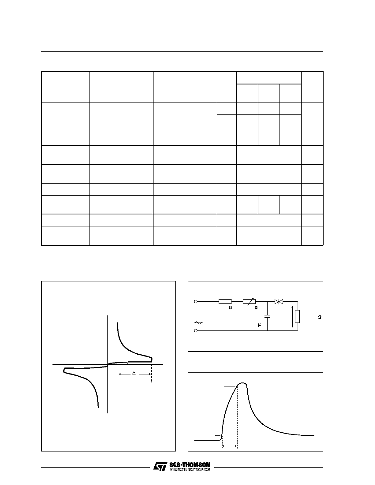
Breakovervoltage* C = 22nF **
MIN 28 30 35 V
seediagram1
TYP 32 34 40
MAX 36 38 45
[I+V
I-I-VBOI] Breakovervoltage
BO
symmetry
I∆V±I Dynamicbreakover
voltage *
V
I
O
BO
Output voltage* see diagram 2 MIN 5 V
Breakovercurrent * C = 22nF** MAX 100 50 100 µA
C = 22nF **
seediagram1
∆I=[I
to IF=10mA]
BO
seediagram1
MAX ± 3V
MIN 5 V
tr Rise time* seediagram3 TYP 1.5 µs
I
B
Leakagecurrent* VB=0.5VBOmax
MAX 10 µA
seediagram1
* Electrical characteristic applicable inboth forward andreverse directions.
** Connected in parallel with the devices.
DIAGRAM 1 : Current-voltagecharacteristics DIAGRAM 2: Test circuitfor outputvoltage
+I
F
10mA
I
BO
-V + V
I
B
0,5 V
BO
V
-I
F
2/4
220 V
50 Hz
10 k 500 k
0.1 F
D.U.T
R=20
V
O
DIAGRAM3 :Testcircuit see diagram2.
AdjustRforlp=0.5A
l
V
BO
90 %
10 %
t
r
p

DB3/ DB4 / DC34
Fig.1: Powerdissipationversusambient tempera-
ture (maximum values)
P (mW)
160
140
120
100
80
60
40
20
0
0 102030405060708090100110120130
o
o
Tamb ( C)
Fig.3 : Peak pulse current versus pulse duration
(maximum values)
I (A)
TRM
2
1
F = 100 Hz
Tj initial = 25 C
o
Fig.2 : Relative variation of VBOversus junction
temperature(typicalvalues)
VBO[Tj]
VBO[Tj=25 C]
1.08
1.06
1.04
1.02
1.00
25 50 75 100 125
o
o
Tj( C)
0.1
tp ( s)
0.01
10 100 1000 10000
3/4
DB3 / DB4 / DC34
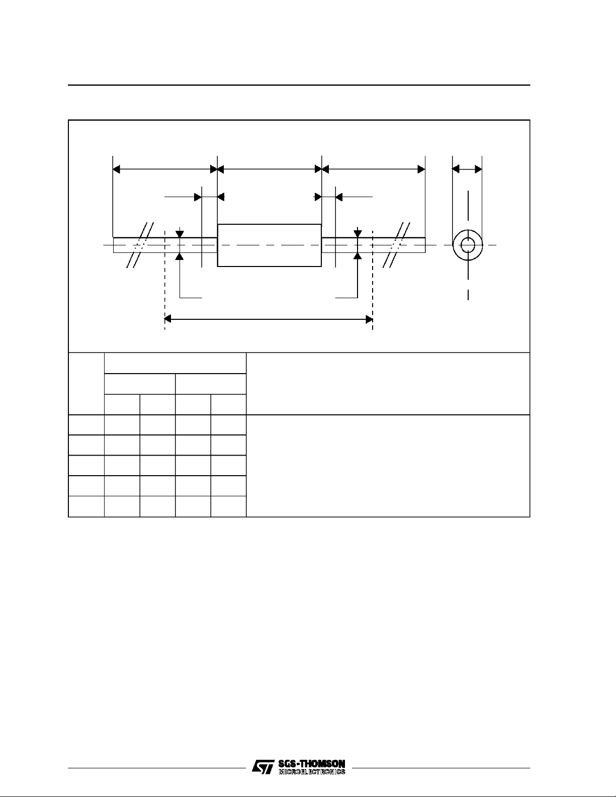
PACKAGEMECHANICAL DATA (in millimeters)
DO 35 Glass
BA B
note 1
/
O
E
D
E
O/
note 1
D
note 2
REF. DIMENSIONS NOTES
Millimeters Inches
Min. Max. Min. Max.
A 3.050 4.500 0.120 0.117
B 12.7 0.500
∅ C 1.530 2.000 0.060 0.079
1 - The lead diameter∅ Disnot controlledoverzoneE
2 - The minimum axiallengh within which the devicemaybe
placedwith its leads bent at right angles is0.59”(15 mm)
/
C
O
∅ D 0.458 0.558 0.018 0.022
E 1.27 0.050
Cooling methodbyconvectionand conduction
Marking: type number
Polarity : N A
Stud torque: N A
Weight: 0.15 g
Information furnished isbelieved to beaccurate and reliable. However, SGS-THOMSON Microelectronics assumes no responsability for the
consequences of use of such information nor for any infringement of patents or other rights of third parties which mayresult from itsuse. No
license is granted by implication or otherwise under any patent orpatent rights of SGS-THOMSON Microelectronics.Specifications mentioned
in thispublication are subject to change without notice. This publication supersedesand replaces all information previously supplied.
SGS-THOMSON Microelectronicsproducts arenotauthorized for use as critical componentsinlife supportdevices orsystemswithout express
written approval of SGS-THOMSON Microelectronics.
1995SGS-THOMSON Microelectronics -All rightsreserved.
2
C Components by SGS-THOMSON Microelectronics, conveys a license under the Philips
2
the I
C Standard Specifications as defined by Philips.
SGS-THOMSON Microelectronics GROUPOF COMPANIES
Singapore -Spain - Sweden- Switzerland - Taiwan - Thailand - UnitedKingdom -U.S.A.
4/4
Purchase ofI
2
I
C Patent.Rights to usethese components in anI2C system,is granted provided that the system conforms to
Australia -Brazil - France - Germany - Hong Kong- Italy - Japan -Korea - Malaysia- Malta -Morocco - The Netherlands -
 Loading...