®
DALC208SC6
Application Specific Discretes
A.S.D.
MAIN APPLICATIONS
Where ESD and/or over and undershoot protection
for datalines is required :
Sensitive logic input protection
Microprocessor based equipment
Audio / Video inputs
Portable electronics
Networks
ISDN equipment
USB interface
DESCRIPTION
The DALC208SC6 diode array is designed to
protect components which are connected to data
and transmission lines from overvoltages caused
by electrostatic discharge (ESD) or other
transients. It is a rail-to-rail protection device also
suited for overshoot and under shoot suppression
on sensitive logic inputs.
The low capacitance of the DALC208SC6
prevents from significant signal distortion.
TM
LOW CAPACITANCE
DIODE ARRAY
1
SOT23-6L (SC74)
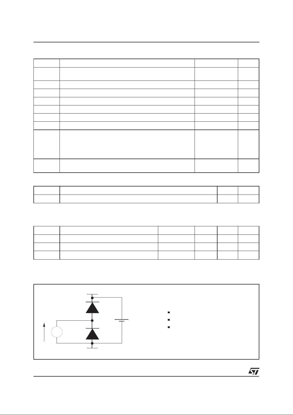
FUNCTIONAL DIAGRAM
FEATURES
PROTECTION OF 4 LINES
PEAK RE VER SE V OLTA GE :
= 9 V per diode
V
RRM
VERY LOW CA PA CIT ANCE PER DIODE:
C < 5 pF
VERY LOW LEAKAGE CURRE NT: IR < 1 µA
BENEFITS
Cost-effectiveness compared to discrete solution
High efficiency in ESD s uppression
No significant signal distortion thanks to very low
capacitance
High reliability offered by monolithic integration
Lower PCB area consumption versus discrete
solution
February 1999 - Ed: 3A
I/O 1
REF 2 REF 1
I/O 2 I/O 3
COMPLIES WITH THE FOLLOWING STANDARDS :
IEC 1000- 4-2 level 4
MIL STD 883C - M ethod 3015-6
(human body test) class 3
I/O 4
1/10

DALC208SC6
ABSOLUTE MAXIMUM RATINGS
(T
= 25° C) .
amb
Symbol Parameter Value Unit
V
PP
IEC1000-4-2, air discharge
IEC1000-4-2, contact discharge
V
RRM
∆
V
REF
max.
V
In
min. Minimum operating signal input voltage V
V
In
I
F
I
FRM
I
FSM
Peak reverse voltage per diode 9 V
Reference voltage gap between V
REF2
and V
REF1
Maximum operating signal input voltage
Continuous forward current (single diode loaded) 200 mA
Repetitive peak forward current (tp = 5 µs, F = 50 kHz)
Surge non repetitive forward current -
15
8
9V
V
REF2
REF1
700 mA
rectangular waveform (see curve on figure 1)
t
= 2.5 µs
p
= 1 ms
t
p
= 100 ms
t
p
T
stg
T
j
Storage temperature range
Maximum junction temperature
6
2
1
-55 to + 150
150
THERMAL RESISTANCE
Symbol Parameter Value Unit
R
th(j-a)
Note 1:
device mounted on FR4 PCB with recommended footprint dimensions.
Junction to ambient (note 1)
500 ° C/W
kV
V
V
A
°
°
C
C
ELECTRICAL CHARACTERI STICS
(T
= 25° C) .
amb
Symbol Parameter Conditions Typ. Max. Unit
V
F
I
R
C
Note 2:
The dynamical behavior is described in the Technical Information section, on page 4.
Note 3:
Forward voltage IF = 50 mA 1.2 V
Reverse leakage current per diode VR = 5 V 1
Input capacitance between Line and G ND see note 3 7 pF
Input capacitance measurement
REF2
REF1 connected to GND
I/O
+V
CC
REF2 connected to +Vcc
Input applied :
R
V
G
Vcc = 5V,Vsign = 30 mV, F = 1 MH z
REF1
µ
A
2/10

DALC208SC6
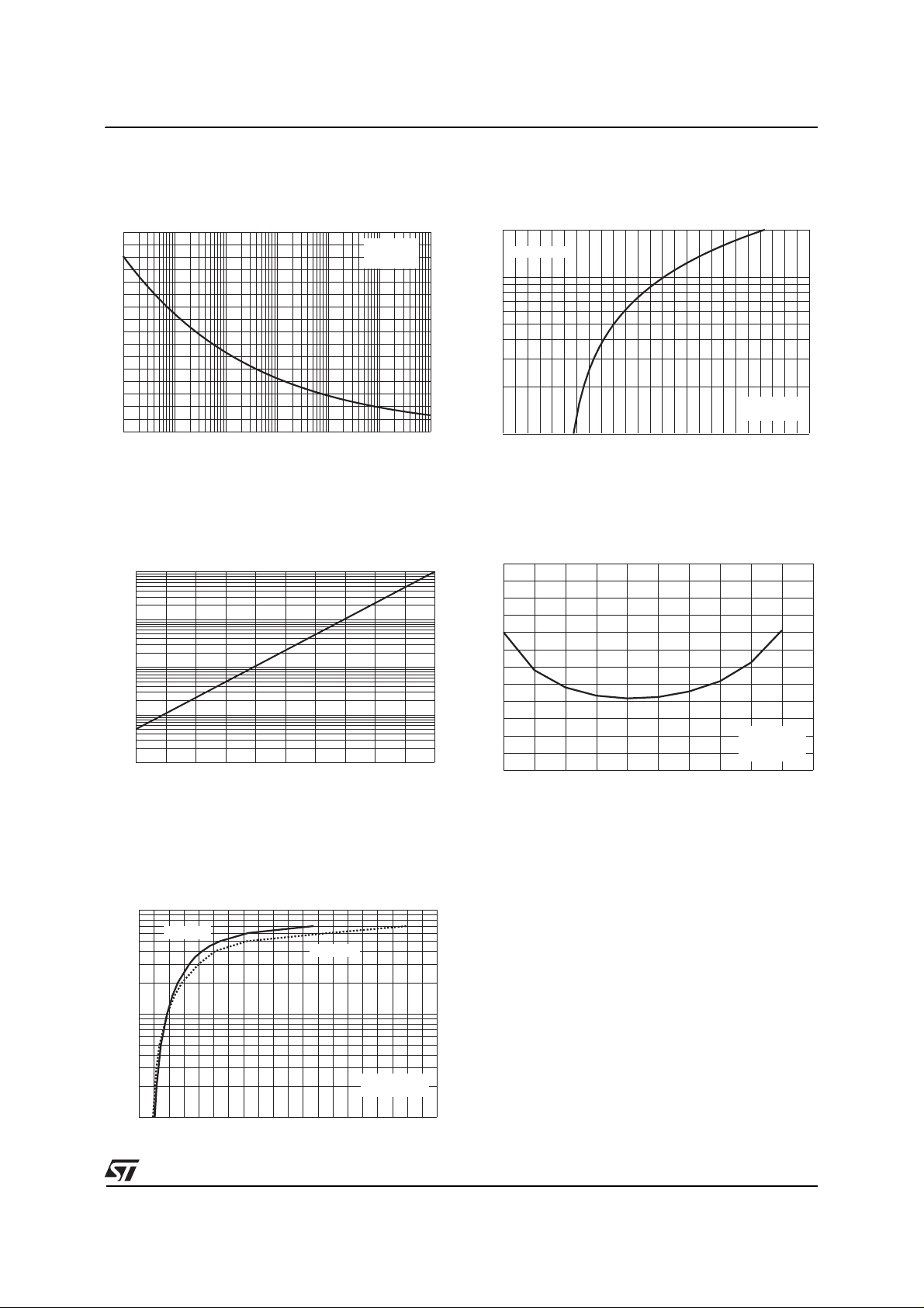
Fig. 1:
Maximum non-repet itive pea k forwar d curre nt
versus rec tangular puls e duration (Tj initial = 25°C).
IFSM(A)
8
7
I/O vs
REF1 or
REF2
6
5
4
3
2
1
0
0.001 0.01 0.1 1 10 100 1000
tp(ms)
Fig. 3:
Variation of leakage current versus junction
temperature (typical values).
IR(µA)
100
10
Fig. 2:
Reverse clamping voltage versus peak
pulse current (Tj initial = 25°C), typical values.
Rectangular waveform tp = 2.5 µs.
Ipp(A)
2.0
tp=2.5µs
1.0
I/O vs REF1
or REF2
0.1
5 1015202530
Vcl(V)
Fig. 4:
Input capacitance versus reverse applied
voltage (typical values).
C(pF)
8.0
7.5
7.0
1
0.1
0.01
25 50 75 100 125 150
Tj(°C)
Fig. 5:
Peak forward voltage drop versus peak forward current (typical values).
Rectangular waveform tp = 2.5 µs.
IFM(A)
10.0
Tj=25°C
Tj=150°C
1.0
I/O vs REF 1
or REF2
6.5
6.0
5.5
5.0
012345
F=1MHz
Vsign=30mV
Vref1/ref2=5V
VR(V)
0.1
0 2 4 6 8 10 12 14 16 18 20
VFM(V)
3/10
 Loading...