

SGS Thomson Microelectronics BZW50-82B, BZW50-47, BZW50-39B, BZW50-39, BZW50-33B Datasheet
...
®
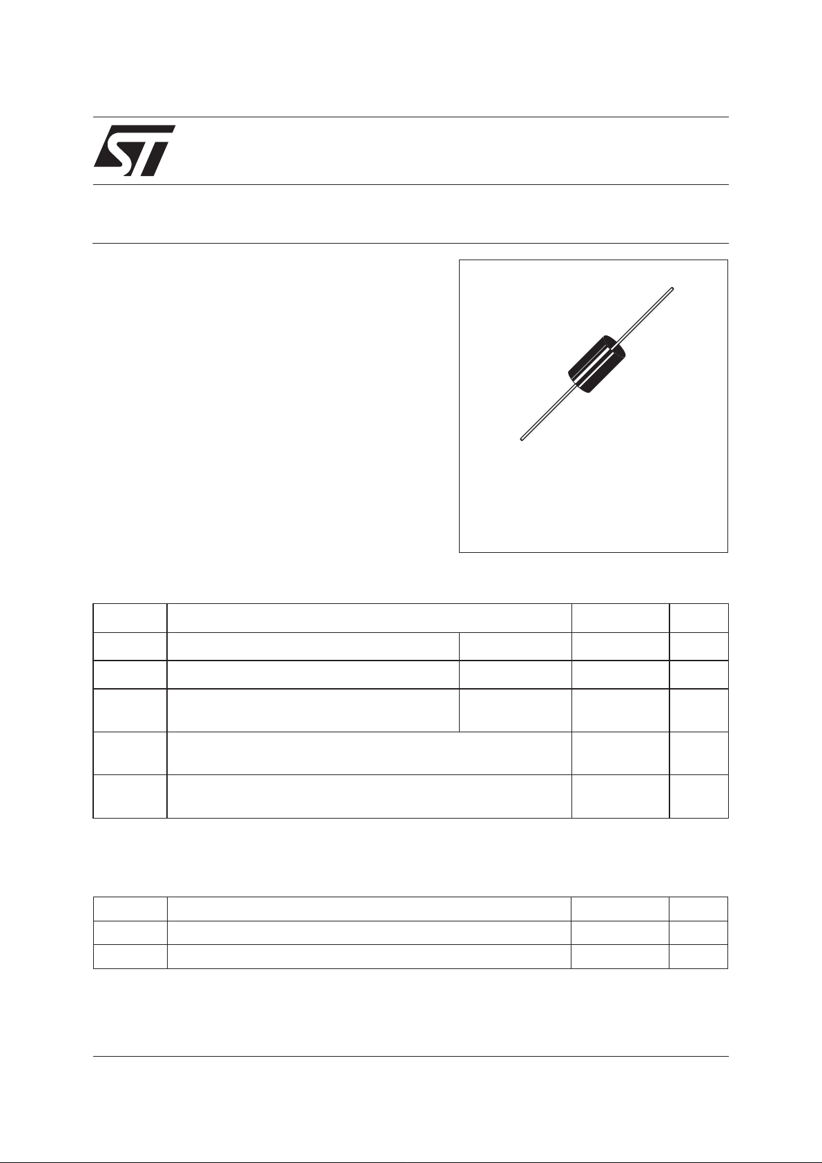
BZW50-10,B/180,B
TRANSIL
FEATURES
PEAK PULSE POWER : 5000 W (10/1000µs)
■
STAND-OFF VOLTAGE RANGE :
■
From 10V to 180V
UNI AND BIDIRECTIONAL TYPES
■
LOW CLAMPING FACTOR
■
FAST RESPONSE TIME
■
UL RECOGNIZED
■
DESCRIPTION
Transil diodes provide high overvoltage protection
by clamping action. Their instantaneous response
to transient overvoltages makes them particularly suited to protect voltage sensitive devices
such as MOS Technology and low voltage supplied IC’s.
ABSOLUTE MAXIMUM RATINGS (T
amb
= 25°C)
Symbol Parameter Value Unit
R6
TM
P
I
FSM
T
T
PP
P
stg
T
L
Peak pulse power dissipation (see note 1) Tj initial = T
Power dissipation on infinite heatsink T
Non repetitive surge peak forward current
for unidirectional types
Storage temperature range
Maximum junction temperature
j
Maximum lead temperature for soldering during 10s at 5mm
= 75°C
amb
tp = 10ms
Tj initial = T
amb
amb
5000 W
6.5 W
500 A
-65to+175
175
230 °C
from case
Note 1 :For a surge greater than the maximum values, the diode will fail in short-circuit.
THERMAL RESISTANCES
Symbol Parameter Value Unit
R
th (j-l)
R
th (j-a)
February 2003- Ed : 4A
Junction to leads
Junction to ambient on printed circuit. L
lead
=10mm
15 °C/W
65 °C/W
°C
°C
1/5
BZW50-10,B/180,B
ELECTRICAL CHARACTERISTICS (T
Symbol Parameter
V
V
V
I
I
αT
RM
BR
CL
RM
PP
V
Stand-off voltage
Breakdown voltage
Clamping voltage
Leakage current @ V
Peak pulse current
Voltage temperature coefficient
Forward voltage drop
F
Types IRM@V
RM
amb
RM
= 25°C)
VBR@I
R
VVCLV
VCL@I
BR
PP
I
I
F
V
RM
I
RM
I
PP
VCL@I
V
F
PP
αTC
max min max max max typ
note2 10/1000µs 8/20µs note3 note4
-4
Unidirectional Bidirectional µAVVmAVAVA10
BZW50-10 BZW50-10B
BZW50-12 BZW50-12B
BZW50-15 BZW50-15B
BZW50-18 BZW50-18B
BZW50-22 BZW50-22B
BZW50-27 BZW50-27B
BZW50-33 BZW50-33B
BZW50-39 BZW50-39B
BZW50-47 BZW50-47B
BZW50-56 BZW50-56B
BZW50-68 BZW50-68B
BZW50-82 BZW50-82B
BZW50-100 BZW50-100B
BZW50-120 BZW50-120B
BZW50-150 BZW50-150B
BZW50-180 BZW50-180B
5 10 11.1 1 18.8 266 23.4 2564 7.8 24000
5 12 13.3 1 22 227 28 2143 8.4 18500
5 15 16.6 1 26.9 186 35 1714 8.8 13500
5 18 20 1 32.2 155 41.5 1446 9.2 11500
5 22 24.4 1 39.4 127 51 1177 9.6 8500
5 27 30 1 48.3 103 62 968 9.8 7000
5 33 36.6 1 59 85 76 789 10 5750
5 39 43.3 1 69.4 72 90 667 10.1 4800
5 47 52 1 83.2 60.1 108 556 10.3 4100
5 56 62.2 1 99.6 50 129 465 10.4 3400
5 68 75.6 1 121 41 157 382 10.5 3000
5 82 91 1 145 34 189 317 10.6 2600
5 100 111 1 179 28 228 263 10.7 2300
5 120 133 1 215 23 274 219 10.8 1900
5 150 166 1 269 19 343 175 10.8 1700
5 180 200 1 322 16 410 146 10.8 1500
/°C pF
V
%I
PP
100
50
0
Note 2 : Pulse test: tp<50ms.
Note 3 : ∆VBR= αT*(T
Note 4 : VR= 0 V, F = 1 MHz. For bidirectional types,
capacitance value is divided by 2.
10 s
PULSE WAVEFORM 10/1000 s
1000 s
- 25)*VBR(25°C)
amb
2/5
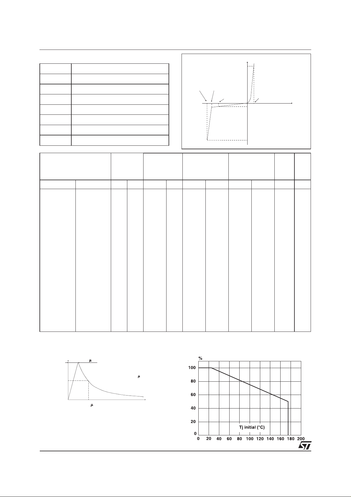
Fig. 1: Peak pulse power dissipation versus initial
junction temperature (printed circuit board).
t
 Loading...