

BYT08P-400
®
FAST RECOVERY RECTIFIER DIODES
MAIN PRODUCT CHARACTERISTI CS
I
F(AV)
V
RRM
(max) 1.4 V
V
F
trr (max) 35 ns
FEATURES AND BENE FITS
VERY LOW RE VE RS E RE COV ER Y T IME
VERY LOW SWITCHING LOSSE S
LOW NOISE TURN-OFF SWITCHING
INSULATED PACKAGE: TO-220AC
Insulation voltage: 2500 V
RMS
Capacitance = 7 pF
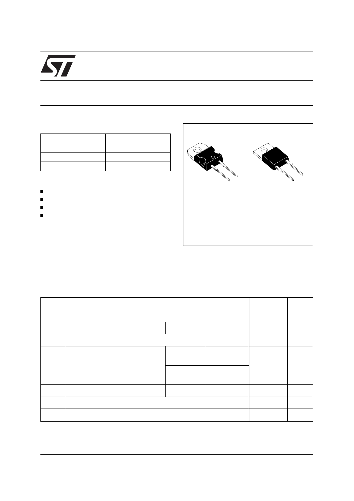
DESCRIPTION
8 A
400 V
T0-220AC
(Plastic)
BYT08PI-400
A
K
Insulated
TO-220AC
(Plastic)
A
K
This single rectifier is suited for Switch Mode
Power Supplies and other power converters.
This device is intended to free-wheeling function in
converters and motor control circuits.
ABSOLUTE RATINGS (limiting values)
Symbol Parameter Value Unit
V
RRM
I
FRM
I
F(RMS)
I
F(AV)
Repetitive peak reverse voltage
Repetitive peak forward current tp=5 µ s F=5kHz
RMS forward current
Average forward current TO-220AC Tc = 120°C
400 V
200 A
16 A
8A
δ = 0.5
Insulated
Tc = 105°C
TO-220AC
I
FSM
T
Tj
stg
Surge non repetitive forward current tp = 10 ms Sinusoidal
Storage temperature range
Maximum operating junction temperature
100 A
- 40 to + 150 °C
150 °C
October 1999 - Ed: 3A
1/7

BYT08P-400 / BYT08PI-400
THERMA L RE SISTA NC ES
Symbol Parameter Value Unit
R
th (j-c)
Junction to case TO-220AC
Ins. TO-220AC
2.5
3.5
STATIC ELECTRICAL CHARACTE RISTICS
Symbol Parameter Test Conditions Min. Typ. Max. Unit
V
*
F
I
**
R
Forward voltage drop Tj = 25°CI
Reverse leakage
current
Pulse test : * tp = 380 µs, δ < 2%
** tp = 5 ms, δ < 2%
= 8 A
F
Tj = 100°C
Tj = 25°CV
= V
R
RRM
Tj = 100°C
1.5 V
1.4
15 µA
2.5 mA
To evaluate the conduction losses use the following equation:
P = 1.1 x I
F(AV)
+ 0.024 I
F2(RMS)
°C/W
RECOVERY CHARAC TERISTICS
Symbol Test Conditions Min. Typ. Max. Unit
t
rr
Tj = 25°C IF = 1A VR = 30V dIF/dt = - 15A/µs
= 0.5A IR = 1A Irr = 0.25A
I
F
75 ns
35
TURN-OFF SWITCHING CHARAC TERISTICS
Symbol Parameter Test Conditions Min. Typ. Max. Unit
75 ns
50
2.2 A
2.8
3.3 /
C =
t
IRM
I
RM
Maxim um reve rse
recovery time
Maxim um reve rse
recovery current
V
V
Turn-off overvo ltage
RP
coefficient
CC
dIF/dt = - 32 A/µ sV
dI
/dt = - 64 A/µ s
F
dIF/dt = - 32 A/µ s
/dt = - 64 A/µ s
dI
F
Tj = 100°C
VCC
= 60V IF = I
= 200 V
CC
I
= 8 A
F
L
≤ 0.05 µH
p
Tj = 100°C
(see fig. 13)
F(AV)
dIF/dt = - 30A/µs Lp = 1µH
2/7
BYT08P-400 / BYT08PI-400
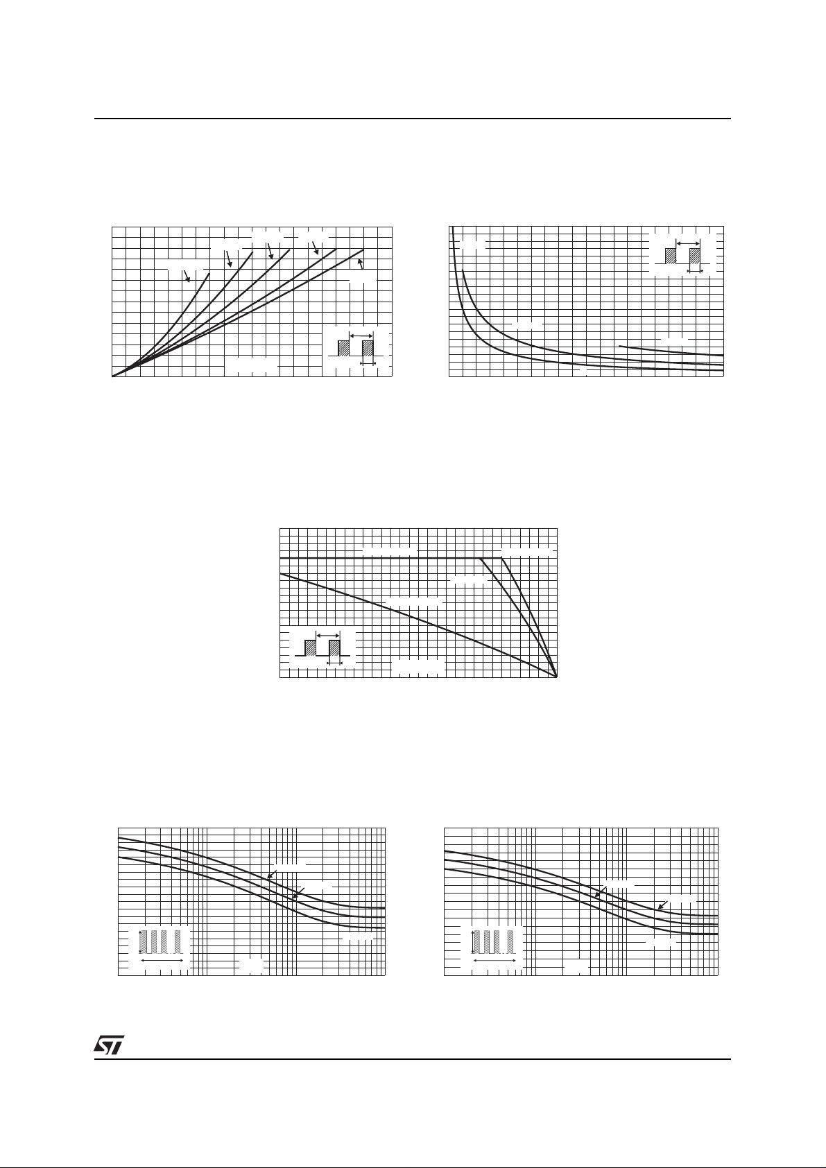
Fig. 1: Average forward power dissipation versus
average forward current .
PF(av)(W)
14
12
10
δ = 0.05
δ = 0.1
δ = 0.2
δ = 0.5
δ = 1
8
6
δ
=tp/T
T
tp
4
2
0
012345678910
IF(av) (A)
Fig. 3: Average forward current versus ambient
temperature (δ=0.5).
IF(av)(A)
10
9
8
7
6
5
4
3
2
1
=tp/T
δ
0
0 25 50 75 100 125 150
Rth(j-a)=Rth(j-c)
T
tp
Fig. 2: Peak current ve r su s f o rm f a ct or.
IM(A)
100
90
P=5W
80
70
60
50
Rth(j-a)=15°C/W
Tamb(°C)
40
30
20
10
0
0.0 0.1 0.2 0.3 0.4 0.5 0.6 0.7 0.8 0.9 1.0
Insulated
P=10W
Non insulated
T
δ
=tp/T
tp
P=20W
δ
Fig. 4-1: Non repetitive surge peak forward current
versus overload duration (TO-220AC).
IM(A)
100
90
80
70
60
50
40
30
I
M
20
10
0
1E-3 1E-2 1E-1 1E+0
t
δ
=0.5
Tc=25°C
Tc=50°C
Tc=75°C
t(s)
Fig. 4-2: Non repetitive surge peak forward current
versus overload duration (insulated TO-220AC).
IM(A)
90
80
70
60
50
40
30
I
M
20
10
0
1E-3 1E-2 1E-1 1E+0
t
δ
=0.5
Tc=50°C
Tc=25°C
Tc=75°C
t(s)
3/7

BYT08P-400 / BYT08PI-400
Fig. 5: Relative variation of thermal impedance
junction to case versus pulse duration.
K=[Zth(j-c)/Rth(j-c)]
1.0
δ = 0.5
0.5
δ = 0.2
δ = 0.1
0.2
Single pulse
tp(s)
0.1
1E-3 1E-2 1E-1 1E+0
δ
=tp/T
T
tp
Fig. 7: Junction capacitance versus reverse
voltage applied (typical values, per diode).
C(pF)
30
28
26
24
22
20
18
16
14
12
10
1 10 100 200
VR(V)
F=1MHz
Tj=25°C
Fig. 6: Forward voltage drop versus forward
current (maximum values, per diode).
IFM(A)
100.0
Typical values
Tj=100°C
10.0
Tj=25°C
1.0
Tj=100°C
0.1
0.0 0.5 1.0 1.5 2.0 2.5 3.0 3.5
Fig. 8: Recovery charges versus dI
Qrr(nC)
250
200
150
100
50
IF=IF(av)
90% confidence
Tj=100°C
0
10 20 50 100 200
VFM(V)
dIF/dt(A/µs)
/dt (per diode).
F
Fig. 9: Recovery current versus dI
/dt (per diode).
F
IRM(A)
10
IF=IF(av)
90% confidence
Tj=100°C
8
6
4
2
dIF/dt(A/µs)
0
10 20 50 100 200
4/7
Fig. 10: Transient peak forward voltage versus
dI
/dt (per diode)
F
VFP(V)
30
IF=IF(av)
90% confidence
Tj=100°C
25
20
15
10
5
0
0 100 200 300 400 500
dIF/dt(A/µs)

BYT08P-400 / BYT08PI-400
Fig. 11: Forward recovery time versus dI
diode)
tfr(µs)
1.50
1.25
1.00
90% confidence
/dt (per
F
IF=IF(av)
Tj=100°C
Fig. 12: Dynamic parameters versus junction
temperature.
Qrr;IRM[Tj] / Qrr;IRM[Tj=100°C]
1.50
1.25
1.00
0.75
0.50
0.25
0.00
0 100 200 300 400 500
dIF/dt(A/µs)
0.75
0.50
0.25
0 25 50 75 100 125 150
Fig. 13: Turn-off switching characteristics (without series inductance).
IRM
Qrr
Tj(°C)
Fig. 14: Turn-off switching characteristics (with series inductance).
5/7

BYT08P-400 / BYT08PI-400
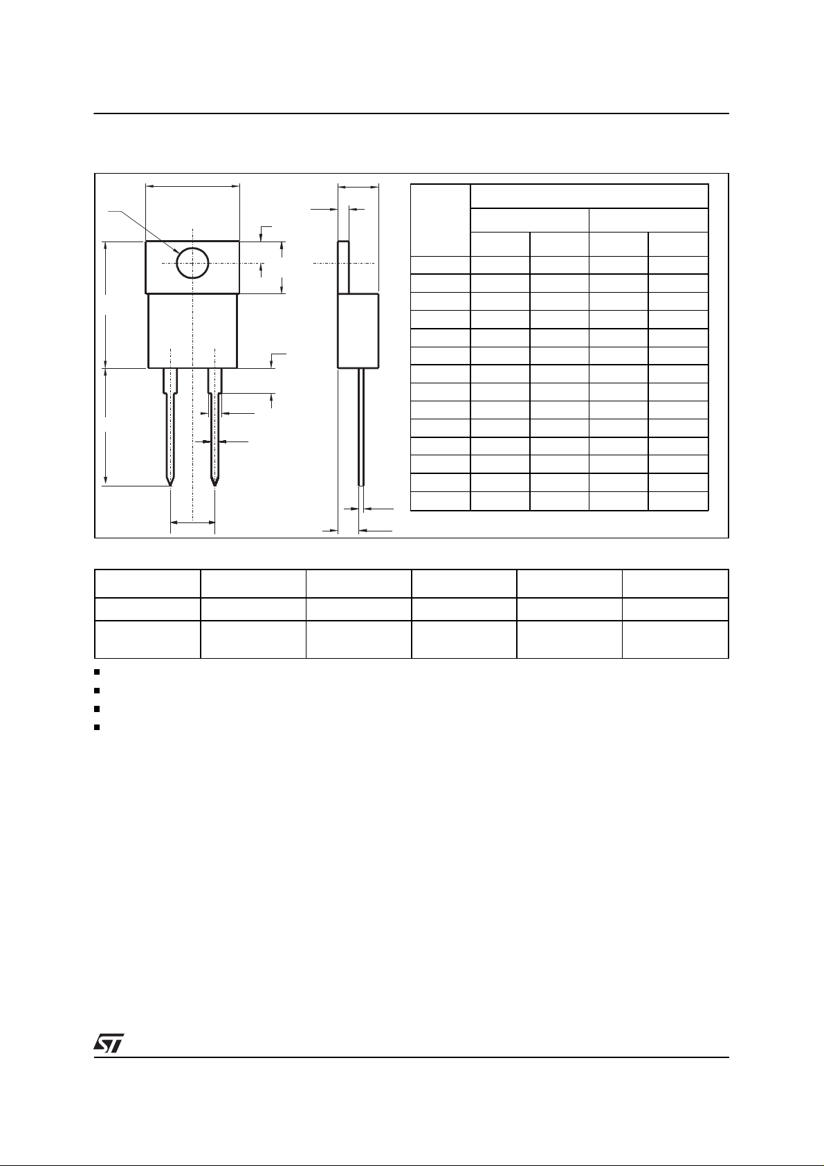
PACKAGE MECHANICAL DATA
TO-220AC
REF.
DIMENSIONS
Millimeters Inches
L2
H2
L5
Ø I
L6
A
C
A 4.40 4.60 0.173 0.181
Min. Max. Min. Max.
C 1.23 1.32 0.048 0.051
L7
D 2.40 2.72 0.094 0.107
E 0.49 0.70 0.019 0.027
F 0.61 0.88 0.024 0.034
F1 1.14 1.70 0.044 0.066
G 4.95 5.15 0.194 0.202
L9
F1
L4
F
D
H2 10.00 10.40 0.393 0.409
L2 16.40 typ. 0.645 typ.
L4 13.00 14.00 0.511 0.551
M
E
L5 2.65 2.95 0.104 0.116
L6 15.25 15.75 0.600 0.620
L7 6.20 6.60 0.244 0.259
G
L9 3.50 3.93 0.137 0.154
M 2.6 typ. 0.102 typ.
Diam. I 3.75 3.85 0.147 0.151
6/7
PACKAGE MECHANICAL DAT A
TO-220AC Insulated
B
I
L
F
A
a1
l2
a2
b1
e
BYT08P-400 / BYT08PI-400
C
b2
REF.
Millimeters Inches
Min. Max. Min. Max.
A 14.23 15.87 0. 560 0.625
a1 4.50 0.177
a2 12.70 14.70 0.500 0.579
B 10.20 10.45 0.402 0.411
b1 0.64 0.96 0.025 0.038
b2 1.15 1.39 0.045 0.055
C 4.48 4.82 0.176 0.190
c1 0.35 0.65 0.020 0.026
c2 2.10 2.70 0.083 0.106
e 4.58 5.58 0.180 0.220
F 5.85 6.85 0.230 0.270
I 3.55 4.00 0.140 0.157
L 2.54 3.00 0.100 0.118
c1
c2
l2 1.45 1.75 0.057 0.069
DIMENSIONS
Ordering type Marking Package Weight Base qty Delivery mode
BYT08P-400 BYT08P-400 TO-220AC 1.86 g. 50 Tube
BYT08PI-400 BYT08PI-400 Insulated
1.86 g. 50 Tube
TO-220AC
Cooling method: by conduction (C)
Recommended torque value: 0.8 N.m.
Maximum torque value: 1.0 N.m.
Epoxy meets UL94,V0
Information furnished is believed to be accurate and reliable. However, STMicroelectronics assumes no responsibility for the consequences of
use of such information nor for any infringement of patents or other rights of third parties which may result from its use. No license is granted by
implication or otherwi se un der any pat ent or patent rights of STMic roelec tronics. S pecifications ment ioned in t his publ ication are subject to
change without notice. This publication supersedes and replaces all information previously supplied.
STMicroelectronics products ar e not authorized for use as critical components in l i fe s upport devices or systems without expres s written approval of STMicroelectronics.
The ST logo is a registered trademark of STMicroe lectronics
© 1999 STMicroelectronics - Printed in Italy - All rights reser ved.
STMicroelectronics GROUP OF COMPANIES
Australia - Brazil - China - Finland - France - Germany - Hong Kong - India - Italy - Japan - Malaysia
Malta - Morocco - Singapore - Spain - Sweden - Switzerland - United Kingdom - U.S.A.
http://www.st.com
7/7
 Loading...