

SGS Thomson Microelectronics BUL116D Datasheet
®
MEDIUM VOLTAGE FAST-SWITCHING
■ INTEGRATED ANTIPARALLEL
COLLECTOR- EMITTER DIODE
■ LOW SPREAD OF DYNAMIC PARAMETERS
■ MINIMUM LOT- TO- LO T SPR E AD FO R
RELIABLE OPERATION
■ VERY H IGH SWITCHING SPEED
APPLICATIONS:
■ COMPACT FLUO RES CENT LAMPS UP T O
23 W AT 110 V A.C. MAINS
■ FLYBACK AND FOR WARD S INGLE
TRANSI ST OR LOW POWER CO N V ERT E RS
AT 110 V A.C. MAINS
DESCRIPTION
The device is manufactured using Multi Epitaxial
Planar technology for high switching speeds and
medium voltage capability.
It uses a Cellular Emitter structure with planar
edge termination to enhance switching speeds
while maintaining the wide RBSOA.
The device is designed for use in lighting
applications and low cost switch-mode power
supplies.
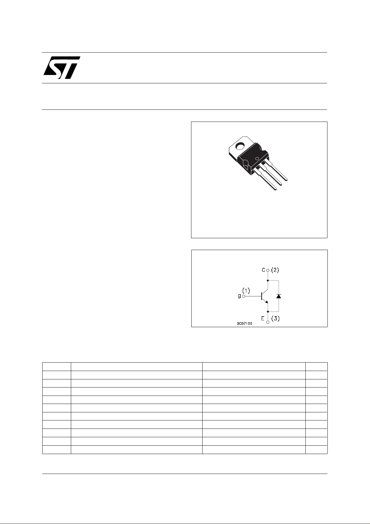
BUL116D
NPN POWER TRANSISTOR
PRELIMINARY DATA
3
2
1
TO-220
INTERNAL SCHEMATIC DIAGRAM
ABSOL UT E MAXIMU M RATINGS
Symbol Parameter Value Unit
V
V
V
I
I
P
T
February 2003
Collector-Emitter Voltage (VBE = 0) 400 V
CES
Collector-Emitter Voltage (IB = 0) 200 V
CEO
Emitter-Base Voltage (IC = 0) 9 V
EBO
Collector Current 5 A
I
C
Collector Peak Current (tp < 5 ms) 10 A
CM
Base Current 2 A
I
B
Base Peak Current (tp < 5 ms) 4 A
BM
Total Dissipation at Tc = 25 oC60W
tot
Storage Temperature -65 to 150
stg
Max. Operating Junction Temperature 150
T
j
o
C
o
C
1/6

BUL116D
THERMAL DATA
R
thj-case
R
thj-amb
Thermal Resistance Junction-Case Max
Thermal Resistance Junction-Ambient Max
2.08
62.5
o
C/W
o
C/W
ELECTRICAL CHARACTERISTICS (T
= 25 oC unless otherwise specified)
case
Symbol Parameter Test Conditions Min. Typ. Max. Unit
I
CES
V
V
CEO(sus)
EBO
Collector Cut-off
Current (V
BE
= 0)
Emitter-Base Voltage
(I
= 0)
C
∗ Collector-Emitter
= 400 V
V
CE
V
= 400 V Tc = 125 oC
CE
= 10 mA 9 V
I
E
I
= 100 mA 200 V
C
100
500
Sustaining Voltage
(I
= 0)
B
I
V
CE(sat)
CEO
Collector Cut-off
Current (I
= 0)
B
∗ Collector-Emitter
Saturation Voltage
V
∗ Base-Emitter
BE(sat)
Saturation Voltage
h
∗ DC Current Gain IC = 10 mA VCE = 5 V
FE
RESISTIVE LOAD
Rise Time
t
r
Fall Time
t
f
t
Storage Time
s
INDUCTIVE LOAD
t
V
∗ Pulsed: Pulse duration = 300 µs, duty cycle 1.5 %
Storage Time
s
Fall Time
t
f
Diode Forward Voltage IC = 2 A 1.5 V
F
= 200 V 250 µA
V
CE
IC = 0.5 A IB = 50 mA
I
= 1 A IB = 0.1 A
C
I
= 3 A IB = 0.6 A
C
I
= 5 A IB = 1 A
C
IC = 1 A IB = 0.1 A
I
= 5 A IB = 1 A
C
0.25
0.4
0.7
1.2
1.1
1.5
10
I
= 5 A VCE = 5 V
C
V
= 125 V IC = 2 A
CC
I
= 0.4 A IB2 = -0.4 A
B1
= 30 µs (see figure 2)
t
p
820
0.2
0.2
0.4
1.4
IC = 2 A IB1 = 0.4 A
= -5 V L = 500 µH
V
BE
V
= 180 V (see figure 1)
clamp
0.5
0.1
µA
µA
V
V
V
V
V
V
µs
µs
µs
µs
µs
Safe Operating Are a Derating Curve
2/6
 Loading...