


BD241BFP
BD242BFP
COMPLEMENTARY SILICON POWER TRANSISTORS
■ SGS-THOMSON PREFERRED SALESTYPES
■ COMPLEMENTARYPNP - NPNDEVICES
■ FULLYMOLDED ISOLATEDPACKAGE
■ 2000V DC ISOLATION(U.L. COMPLIANT)
APPLICATIONS
■ GENERALPURPOSESWITCHING
■ GENERALPURPOSEAMPLIFIERS
3
DESCRIPTION
The BD241BFP is silicon epitaxial-base NPN
transistors mounted in TO-220FP fully molded
isolated package.
It is inteded for power linear and switching
applications.
The complementaryPNP types is the BD242BFP.
TO-220FP
2
1
INTERNAL SCHEMATIC DIAGRAM
ABSOLUTE MAXIMUM RATINGS
Symbol Parameter Value Unit
NPN BD241BFP
PNP BD242BFP
V
V
V
I
P
T
For PNP types voltage and current values are negative.
Collect or- B as e Voltage (RBE=100Ω)90V
CER
Collector-Emitter Voltage ( IB=0) 80 V
CEO
Emitter-Base Voltage (IC=0) 5 V
EBO
Collect or Current 3 A
I
C
Collect or Peak Current 5 A
CM
Base Current 1 A
I
B
Tot al Diss ipa t ion at Tc≤ 25oC24W
tot
Storage Temperature -65 to 150
stg
Max. Operat ing Juncti on Tem per at u re 150
T
j
o
C
o
C
April 1998
1/4

BD241BFP / BD242BFP
THERMAL DATA
R
thj-case
Ther mal Resistan ce J u nc t io n- case Max 5.3
o
C/W
ELECTRICAL CHARACTERISTICS (T
=25oC unlessotherwise specified)
case
Symbol Parameter Test Condition s Mi n. Typ. Max. Unit
I
CEO
I
CES
I
EBO
V
CEO(sus)
Collector Cut- of f
Current (I
B
=0)
Collector Cut- of f
Current (V
BE
=0)
Emit ter Cut-o f f Current
(I
=0)
C
∗ Collector-Emitter
V
=60V 0.3 mA
CE
V
=80V 0.2 mA
CE
=5V 1 mA
V
EB
I
=30mA 80 V
C
Sust aining V olt ag e
=0)
(I
B
V
∗ Collector-Emitter
CE(sat)
IC=3A IB= 0.6 A 1.2 V
Saturation Voltage
V
∗
Pulsed: Pulse duration = 300 µs, duty cycle ≤ 2%
For PNP types voltage and current valuesare negative.
∗ Ba se-Emitt er Voltage IC=3A VCE=4V 1.8 V
BE(ON)
h
FE*
DC Current G ain IC=1A VCE=4V
=3A VCE=4V
I
C
25
10
2/4
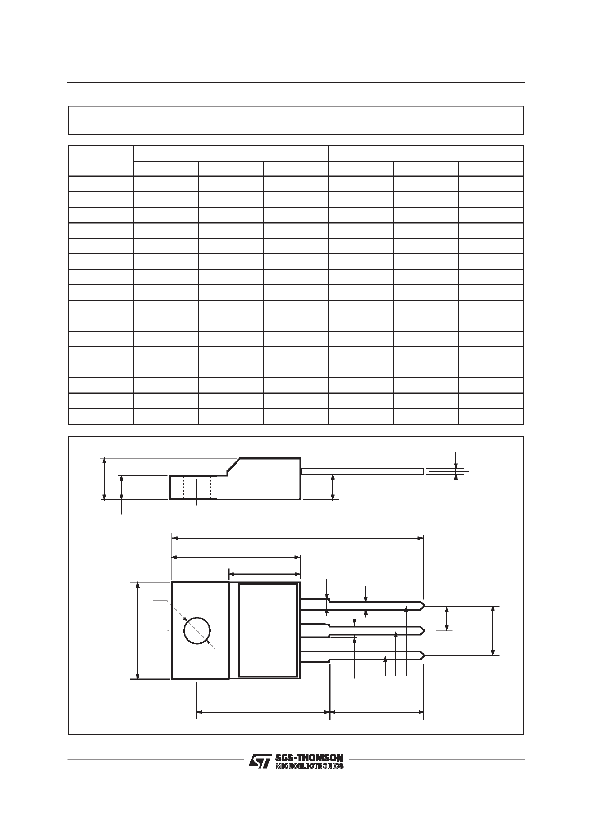
TO-220FP MECHANICAL DATA
BD241BFP / BD242BFP
DIM.
MIN. TYP. MAX. MIN. TYP. MAX.
A 4.4 4.6 0.173 0.181
B 2.5 2.7 0.098 0.106
D 2.5 2.75 0.098 0.108
E 0.45 0.7 0.017 0.027
F 0.75 1 0.030 0.039
F1 1.15 1.7 0.045 0.067
F2 1.15 1.7 0.045 0.067
G 4.95 5.2 0.195 0.204
G1 2.4 2.7 0.094 0.106
H 10 10.4 0.393 0.409
L2 16 0.630
L3 28.6 30.6 1.126 1.204
L4 9.8 10.6 0.385 0.417
L6 15.9 16.4 0.626 0.645
L7 9 9.3 0.354 0.366
Ø 3 3.2 0.118 0.126
mm inch
E
A
D
B
L3
L6
L7
¯
F1
F
G1
H
G
F2
123
L2
L4
3/4

BD241BFP / BD242BFP
Information furnished is believed to be accurate and reliable. However, SGS-THOMSON Microelectronics assumes no responsability for the
consequences of use of such information nor for any infringement ofpatents or other rights of third parties which may results from its use. No
license isgranted byimplication or otherwise under any patent orpatent rights of SGS-THOMSON Microelectronics. Specifications mentioned
in thispublication are subject to change without notice. This publication supersedes and replaces allinformation previously supplied.
SGS-THOMSON Microelectronics products are not authorizedfor useas criticalcomponents in life support devices orsystems without express
written approval of SGS-THOMSON Microelectonics.
1998 SGS-THOMSON Microelectronics - Printed in Italy - All Rights Reserved
Australia - Brazil - Canada -China - France - Germany - Italy - Japan - Korea - Malaysia - Malta - Morocco - The Netherlands -
Singapore - Spain - Sweden - Switzerland - Taiwan - Thailand - United Kingdom - U.S.A
4/4
SGS-THOMSON Microelectronics GROUP OF COMPANIES
...
 Loading...