

SMALL SIGNAL PNP TRANSISTORS
Type Marking
BCW69 H 1
BCW70 H 2
■ SILICONEPITAXIALPLANAR PNP
TRANSISTORS
■ MINIATUREPLASTIC PACKAGEFOR
APPLICATIONIN SURFACE MOUNTING
CIRCUITS
■ LOW LEVEL AUDIO AMPLIFICATIONAND
SWITCHING
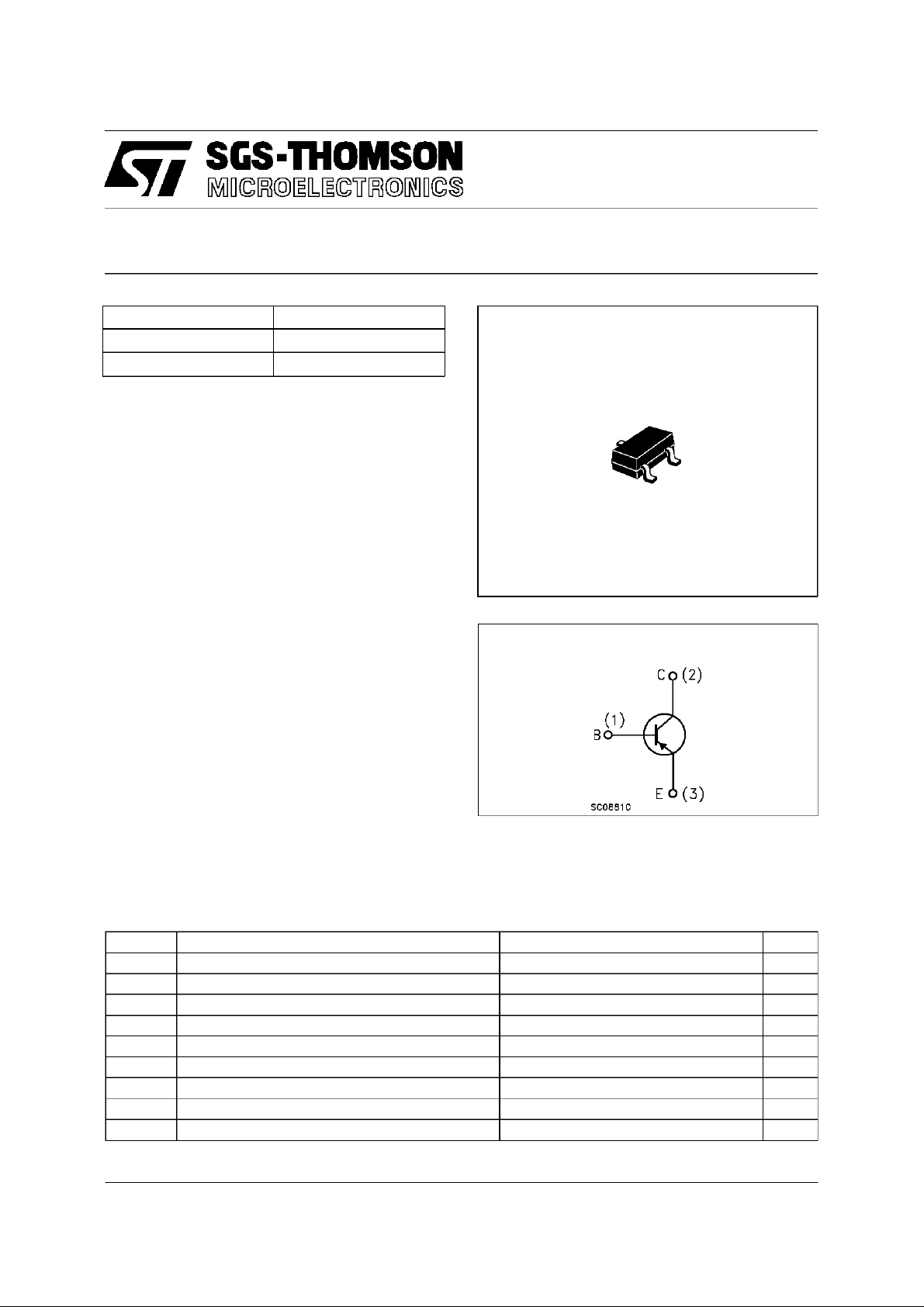
BCW69
BCW70
2
3
1
SOT-23
INTERNAL SCHEMATIC DIAGRAM
ABSOLUTE MAXIMUM RATINGS
Symb o l Parameter Val u e Uni t
V
V
V
V
I
P
T
Collector-Emitter Voltage (VBE=0) -50 V
CES
Collector-Emitter Voltage (IB=0) -45 V
CEO
Collector-Base Voltage (IE=0) -50 V
CBO
Emitter-Base Voltage (IC=0) -5 V
EBO
Collect or Cur rent -0. 1 A
I
C
Collect or P eak Current -0. 2 A
CM
Total Dis sipation at Tc=25oC300mW
tot
Stora ge Temperature -65 to 150
stg
Max. O perating J unc t i on Temperatur e 150
T
j
o
C
o
C
March 1996
1/4

BCW69/BCW70
THERMAL DATA
R
• Mounted on a ceramic substrate area = 10 x8 x 0.6mm
• Thermal Resistance Junction-Ambient Max 420
thj-amb
o
C/W
ELECTRICAL CHARACTERISTICS (T
=25oC unlessotherwise specified)
case
Symbol Parameter Test C ondition s Min. Typ. Max. Unit
I
CBO
V
(BR)CES
Collector Cut-of f
Current (I
E
=0)
∗ Collector-Em it t er
V
=-20V
CB
=-20V Tj=100oC
V
CB
I
=-10µA-50V
C
-100
-10
Break dow n Voltage
=0)
(V
BE
V
∗ Co llec tor-Em it t er
(BR) CEO
I
=-2mA -45 V
C
Break dow n Voltage
=0)
(I
B
V
(BR) CBO
∗ Co llec tor-Bas e
I
=-10µA-50V
C
Break dow n Voltage
=0)
(I
E
V
(BR)EBO
Emitt er-Base
I
=-10µA-5V
E
Break dow n Voltage
=0)
(I
C
V
∗ Collector-Em it t er
CE(sat)
Saturation Voltage
V
∗ Collector-Bas e
BE(sat)
Saturation Voltage
V
∗ Base-Emitt er O n
BE(on)
IC=-10mA IB=-0.5mA
=-50mA IB= -2.5 mA -0. 18
I
C
IC=-10mA IB=-0.5mA
=-50mA IB=-2.5mA
I
C
-0.72
-0.81
IC=-2mA VCE= -5 V -0.6 -0.75 V
-0.3 V
Volt age
∗ DC Cur rent Gain for BCW69
h
FE
=-10µAVCE=-5V
I
C
=-2mA VCE=-5V
I
C
120
90
260
for BCW70
=-10µAVCE=-5V
I
C
=-2mA VCE=-5V
I
C
f
C
Tr ansition F r eque ncy IC=-10mA VCE= -5 V f = 100 M Hz 150 MHz
T
CB
Collector Base
IE=0 VCB=-10V f=1MHz 7 dB
215
150
500
Capacit a nc e
NF No is e Fig ure I
∗
Pulsed: Pulse duration = 300 µs,duty cycle≤ 2%
=-0.2mA VCE=-5V f=1KHz
C
∆f = 200 Hz R
=2KΩ
g
10 dB
nA
µA
V
V
V
2/4

SOT-23 MECHANICALDATA
BCW69/BCW70
DIM.
MIN. TYP. MAX. MIN. TYP. MAX.
A 0.85 1.1 33.4 43.3
B 0.65 0.95 25.6 37.4
C 1.20 1.4 47.2 55.1
D 2.80 3 110.2 118
E 0.95 1.05 37.4 41.3
F 1.9 2.05 74.8 80.7
G 2.1 2.5 82.6 98.4
H 0.38 0.48 14.9 18.8
L 0.3 0.6 11.8 23.6
M 0 0.1 0 3.9
N 0.3 0.65 11.8 25.6
O 0.09 0.17 3.5 6.7
mm mils
0044616/B
3/4

BCW69/BCW70
Information furnished is believedto be accurate and reliable. However, SGS-THOMSON Microelectronicsassumes no responsability for the
consequencesof use ofsuch information nor for anyinfringement of patentsor other rights of third parties which may resultsfrom its use. No
licenseis grantedby implicationor otherwise underany patent or patentrights of SGS-THOMSON Microelectronics.Specificationsmentioned
in this publication are subject to change without notice.This publication supersedes andreplaces all information previously supplied.
SGS-THOMSONMicroelectronics productsare notauthorizedfor useascriticalcomponents in life supportdevices or systemswithoutexpress
writtenapproval of SGS-THOMSON Microelectonics.
1995 SGS-THOMSONMicroelectronics- Printedin Italy- All Rights Reserved
Australia- Brazil - Canada- China- France- Germany- Hong Kong- Italy- Japan- Korea- Malaysia- Malta - Morocco- The Netherlands -
Singapore- Spain- Sweden- Switzerland - Taiwan - Thailand - United Kingdom- U.S.A
SGS-THOMSONMicroelectronicsGROUP OF COMPANIES
.
4/4
 Loading...