

HIGH-SPEED SATURATED SWITCH
DESCRIPTION
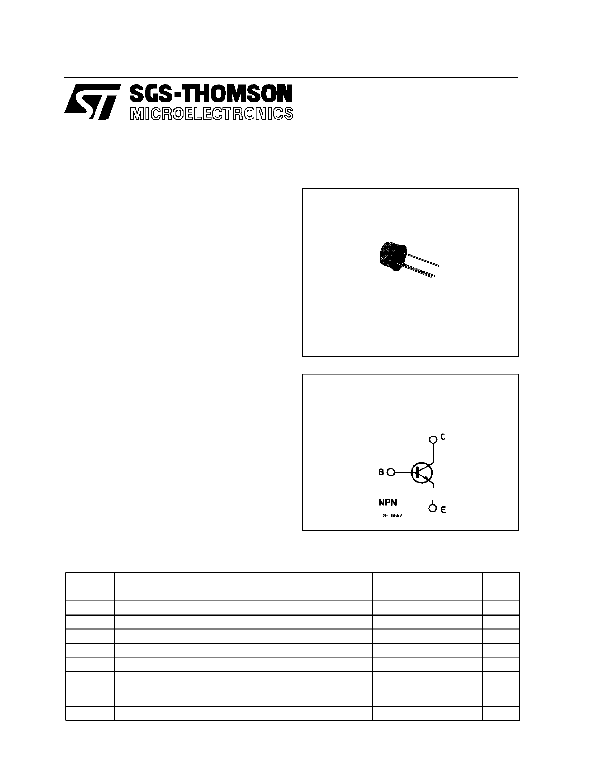
The 2N2369A isa silicon planar epitaxialNPN transistorinJedecTO-18metalcase.Itisdesigned specificallyfor high-speed saturated switching applications at current levels from 100 µA to 100mA.
2N2369A
TO-18
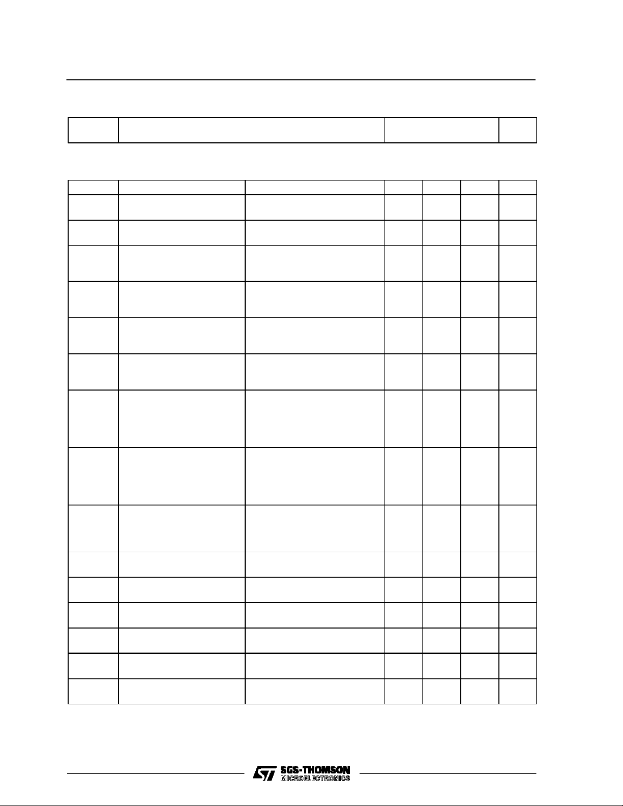
INTERNAL SCHEMATIC DIAGRAM
ABSOLUTE MAXIMUM RATINGS
Symbol Paramet e r Val ue Unit
V
CB O
V
CE S
V
CE O
V
EBO
I
C
I
CM
P
tot
T
stg,Tj
November1988
Collector-base Voltage (IE=0) 40 V
Collector-emitter Voltage (VBE=0) 40 V
Collector-emitter Voltage (IB=0) 15 V
Emitter-base Voltage (IC= 0) 4.5 V
Collector Current 0.2 A
Collector Current (10 µs pulse) 0.5 A
Total Power Dissipation at T
at T
at T
Storage and Junction Temperature – 65 to 200 °C
amb
case
case
≤ 25 °C
≤ 25 °C
≤ 100 °C
0.36
1.2
0.68
W
W
W
1/6
2N2369A
THERMAL DATA
R
th j-case
R
th j-amb
ELECTRICAL CHARACTERISTICS (T
Thermal Resistance Junction-case
Thermal Resistance Junction-ambient
amb
Max
Max
=25°C unlessotherwise specified)
146
486
Symbol Parameter Test Conditions Min. Typ. Max. Unit
I
CBO
I
CES
V
(BR) CBO
V
(BR)CES
V
(BR)CEO
V
(BR) EBO
V
CE (sat )
V
BE (s at)
h
FE
h
FE
f
T
C
CB O
t
s
t
on
t
off
*
Pulsed : pulse duration = 300 µs, duty cycle = 1 %.
Collector Cutoff
Current (IE=0)
Collector Cutoff
Current (V
BE
=0)
V
=20V T
CB
= 20 V 0.4 µA
V
CE
Collector-base
Breakdown Voltage
(I
=0)
E
IC=10µA40 V
Collector-emitter
Breakdown Voltage
(V
=0)
BE
=10µA40 V
I
C
* Collector-emitter
Breakdown Voltage
(I
=0)
B
IC=10mA 15 V
Emitter-base
Breakdown Voltage
(I
=0)
C
* Collector-emitter
Saturation Voltage
=10µA 4.5 V
I
E
IC=10mA
IC=30mA
IC= 100 mA
I
=10mA
C
T
=125°C
amb
* Base-emitter
Saturation Voltage
IC=10mA
IB=30mA
I
= 100 mA
C
IC=10mA
T
=–55
amb
* DC Current Gain IC=10mA
I
=10mA
C
IC=30mA
I
= 100 mA
C
* DC Current Gain IC=10mA
T
=–55°C
amb
Transition Frequency IC=10mA
f=100MHz
Collector-base
Capacitance
IE=0
f=1MHz
** Storage Time IC=10mA
IB1=
–IB2=10mA
** Turn-on Time IC=10mA
IB1=3 mA
** Turn-off Time IC=10mA
I
=3 mA
B1
amb
=1mA
I
B
IB=3mA
IB=10mA
I
=1mA
B
I
=1mA
B
IB=3mA
I
=10mA
B
IB=1mA
to 125 °C
V
CE
V
CE
VCE= 0.4 V
V
CE
V
CE
V
CE
V
CB
VCC=10V
V
CC
V
CC
I
B2
=150°C30µA
= 0.35 V
=1V
=1V
0.7
0.59
40
40
30
20
0.14
0.17
0.28
0.19
0.8
0.9
1.1
63
66
71
0.2
0.25
0.5
0.3
0.85
1.15
1.6
1.02
120
120
= 0.35 V 20 50
= 10 V 500 675 MHz
= 5 V 2.3 4 pF
613ns
=3V 9 12 ns
=3V
= – 1.5 mA
13 18 ns
°C/W
°C/W
V
V
V
V
V
V
V
V
2/6

DC Current Gain. Collector-emitter SaturationVoltage.
Contours of Constant Transition Frequency.Collector-base andemitter-base capacitances.
2N2369A
SwitchingCharacteristics. Switching Characteristics.
3/6

2N2369A
Test Circuitfor t
s
TestCircuitfor ton,t
off
4/6

TO-18 MECHANICAL DATA
2N2369A
DIM.
MIN. TYP. MAX. MIN. TYP. MAX.
A 12.7 0.500
B 0.49 0.019
D 5.3 0.208
E 4.9 0.193
F 5.8 0.228
G 2.54 0.100
H 1.2 0.047
I 1.16 0.045
L45
o
mm inch
o
45
G
I
H
DA
F
E
L
B
C
0016043
5/6

2N2369A
Information furnished is believed to be accurate and reliable. However, SGS-THOMSON Microelectronics assumes no responsability for the
consequences of use of such information nor for any infringementofpatents or other rights of third partieswhich may results from its use. No
license is grantedbyimplicationorotherwiseunder any patent or patent rights of SGS-THOMSON Microelectronics.Specificationsmentioned
in this publication are subject to change without notice. This publication supersedesand replaces all information previouslysupplied.
SGS-THOMSON Microelectronicsproducts arenot authorizedforuse as criticalcomponentsin life supportdevices or systemswithoutexpress
written approval of SGS-THOMSON Microelectonics.
1994SGS-THOMSON Microelectronics- All RightsReserved
Australia - Brazil - France - Germany - Hong Kong -Italy - Japan - Korea - Malaysia - Malta - Morocco- The Netherlands -
Singapore - Spain - Sweden - Switzerland - Taiwan - Thailand - United Kingdom - U.S.A
SGS-THOMSON Microelectronics GROUP OF COMPANIES
6/6
 Loading...