

DESCRIPTION
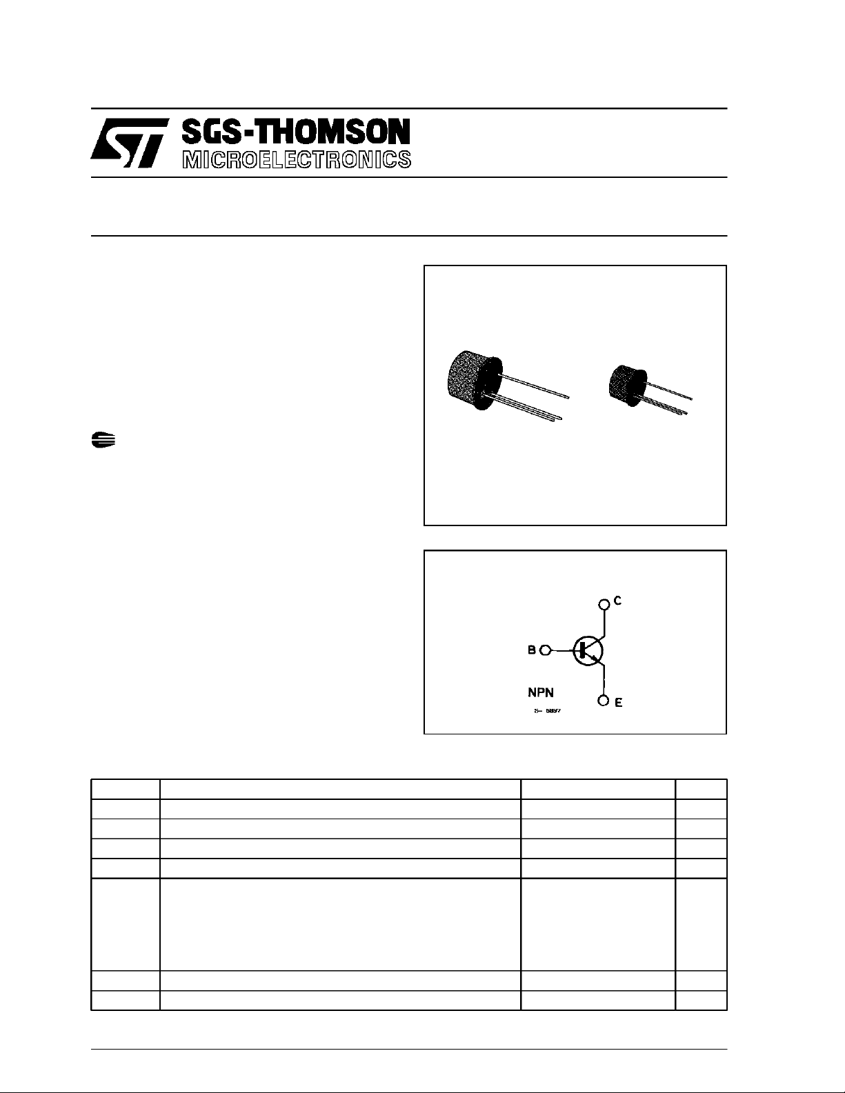
The 2N2218, 2N2219,2N2221 and 2N2222aresilicon planar epitaxial NPN transistors in Jedec
TO-39 (for 2N2218 and 2N2219) and in Jedec
TO-18(for2N2221 and2N2222) metalcases. They
are designed for high-speed switchingapplications
at collectorcurrents upto 500 mA, and featureuseful current gain over a wide range of collector current, low leakage currents and low saturation voltages.
2N2218-2N2219
2N2221-2N2222
HIGH-SPEED SWITCHES
2N2218/2N2219 approved to CECC 50002100, 2N2221/2N2222 approved to CECC
TO-39
TO-18
50002-101 available on request.
INTERNAL SCHEMATIC DIAGRAM
ABSOLUTE MAXIMUM RATIN G S
Symbol Parameter Value Unit
V
V
V
P
T
CBO
CEO
EBO
I
C
tot
stg
T
Collector-base Voltage (IE=0) 60 V
Collector-emitter Voltage (IB=0) 30 V
Emitter-base Voltage (IC=0) 5 V
Collector Current 0.8 A
Total Power Dissipation at T
for 2N2218 and 2N22 19
for 2N2221 and 2N22 22
at T
for 2N2218 and 2N22 19
for 2N2221 and 2N22 22
Storage Temperature – 65 to 200 °C
Junction Temperature 175 °C
j
amb
case
≤ 25 °C
0.8
0.5
≤ 25 °C
3
1.8
W
W
W
W
January 1989
1/5
2N2218-2N2219-2N2221-2N2222
THERMAL DATA
R
th j-case
R
th j-amb
Thermal Resistance Junction-case
Thermal Resistance Junction-ambient
ELECTRICAL CHARACTERISTICS (T
Max
Max
=25°C unless otherwise specified)
amb
2N22 18
2N22 19
50 °C/W
187.5 °C/W
2N222 1
2N222 2
83.3 °C/W
300 °C/W
Symbol Parameter Test Conditions Min. Typ. Max. Unit
I
CBO
I
EBO
V
(BR) CBO
V
(BR)CEO
V
(BR) EBO
V
CE (sat )
V
BE (sat )
h
FE
f
T
C
CBO
R
e(hie)
*
Pulsed : pulse duration = 300 µs, duty cycle = 1 %.
Collector Cutoff Current
(I
=0)
E
Emitter Cutoff Current
(I
=0)
C
Colllector-base Breakdown
Voltage (IE=0)
* Collector-emitter Breakdown
Voltage (IB=0)
Emittter-base Breakdown
Voltage (IC=0)
* Collector-emitter Saturation
Voltage
* Base-emitter Saturation
Voltage
=50V
V
CB
V
=50V T
CB
=3V 10 nA
V
EB
=10µA60V
I
C
I
=10mA 30 V
C
I
=10µA5V
E
IC=150mA
IC=500mA
IC=150mA
I
=500mA
C
* DC Current Gain for 2N2218
I
= 0.1 mA
C
IC=1mA
I
=10mA
C
IC=150mA
IC=500mA
I
=150mA
C
for 2N2219
I
= 0.1 mA
C
IC=1mA
IC=10mA
I
=150mA
C
IC=500mA
I
=150mA
C
Transition Frequency IC=20mA
f = 100 MHz
Collector-base Capacitance IE=0
f = 100 kHz
Real Part of Input
Impedance
IC=20mA
f = 300 MHz
=150°C
amb
IB=15mA
IB=50mA
=15mA
I
B
I
=50mA
B
and 2N2221
V
=10V
CE
VCE=10V
V
=10V
CE
VCE=10V
VCE=10V
V
=1V
CE
and 2N2222
V
=10V
CE
VCE=10V
VCE=10V
V
=10V
CE
VCE=10V
V
=1V
CE
V
= 20 V 250 MHz
CE
V
=10V 8 pF
CB
=20V 60 Ω
V
CE
20
25
35
40
20
20
35
50
75
100
30
50
10
10
0.4
1.6
1.3
2.6
120
300
nA
µA
V
V
V
V
2/5

2N2218-2N2219-2N2221-2N2222
TO-18 MECHANICAL DATA
DIM.
MIN. TYP. MAX. MIN. TYP. MAX.
A 12.7 0.500
B 0.49 0.019
D 5.3 0.208
E 4.9 0.193
F 5.8 0.228
G 2.54 0.100
H 1.2 0.047
I 1.16 0.045
L45
o
mm inch
o
45
G
I
H
DA
F
E
L
B
C
0016043
3/5

2N2218-2N2219-2N2221-2N2222
TO39 MECHANICAL DATA
DIM.
mm inch
MIN. TYP. MAX. MIN. TYP. MAX.
A 12.7 0.500
B 0.49 0.019
D 6.6 0.260
E 8.5 0.334
F 9.4 0.370
G 5.08 0.200
H 1.2 0.047
I 0.9 0.035
o
L45
(typ.)
4/5
I
H
G
F
E
L
DA
B
P008B

2N2218-2N2219-2N2221-2N2222
Information furnished is believed to be accurate and reliable. However, SGS-THOMSON Microelectronics assumes no responsability for the
consequences of use of such information nor foranyinfringementof patents or other rights of third parties which may results from its use. No
license isgrantedby implication orotherwiseunder anypatent or patent rights ofSGS-THOMSON Microelectronics.Specificationsmentioned
in this publication are subject to change without notice. This publication supersedes and replaces all information previouslysupplied.
SGS-THOMSON Microelectronicsproductsarenot authorized foruse ascriticalcomponentsin life supportdevicesorsystems withoutexpress
written approval of SGS-THOMSON Microelectonics.
1994 SGS-THOMSON Microelectronics - All Rights Reserved
Australia - Brazil - France - Germany - Hong Kong - Italy - Japan - Korea - Malaysia - Malta - Morocco - The Netherlands -
Singapore - Spain - Sweden - Switzerland - Taiwan - Thailand - United Kingdom - U.S.A
SGS-THOMSON MicroelectronicsGROUPOF COMPANIES
5/5
 Loading...