®
LOW DROP POWER SCHOTTK Y RECTIFIER
MAIN PRODUCTS CHARACTE RISTICS
1N581x
I
F(AV)
V
RRM
T
j
(max) 0.45 V
V
F
1 A
40 V
150°C
FEATURES AND BENE FITS
VERY SMALL CONDUCTION LOSSES
NEGLIGIBLE SWITCHING LOSSE S
EXTREMELY FAST SWITCHING
LOW FORWARD V O LTAGE DROP
DESCRIPTION
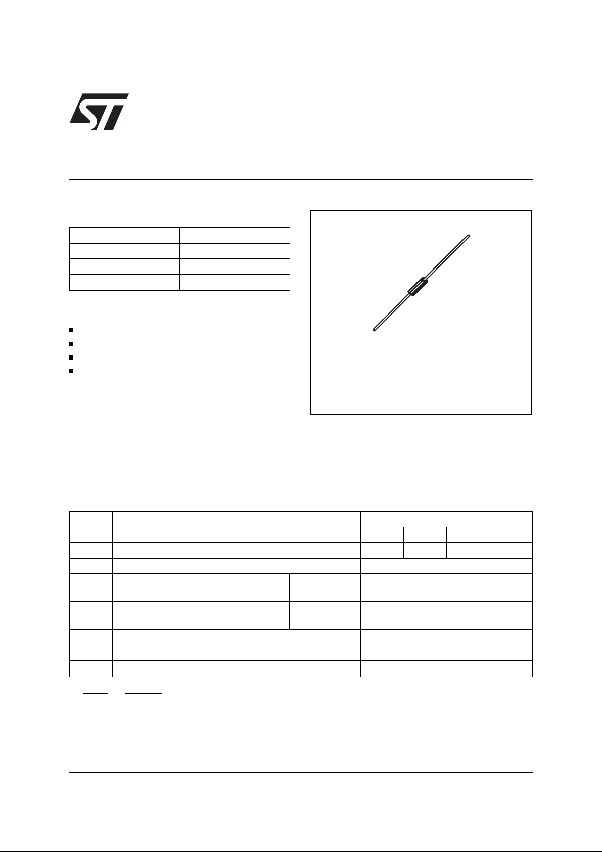
Axial Power Schottky rectifier suited for Switch
Mode Power Supplies and high frequency DC to
DC converters. Packaged in DO41 these devices
are intended for use in low voltage, high frequency
inverters, free wheeling, polarity protection and
small battery chargers.
ABSOLUTE RATINGS (limiting values)
Symbol Parameter
V
RRM
I
F(RMS)
I
F(AV)
I
FSM
T
stg
Tj
dV/dt
Repetitive peak reverse voltage
RMS forward current
Average forward current TL = 125°C
Surge non repetitive forward current tp = 10 ms
Storage temperature range
Maximum operating junction temperature *
Critical rate of rise of rev erse v oltage
δ = 0.5
Sinusoidal
DO41
Value
1N5817 1N5818 1N5819
20 30 40 V
10 A
1A
25 A
- 65 to + 150 °C
150 ° C
10000 V/µs
Unit
dPtot
* :
July 1999 - Ed: 2A
dTj
<
Rth(j−a
1
thermal runaway condition for a diode on its own heatsink
)
1/5

1N581x
THERMA L RE SISTA NC ES
Symbol Parameter Value Unit
R
R
th (j-a)
th (j-l)
Junction to ambient
Junction to lead
STATIC ELECTRICAL CHARACTE RISTICS
Symbol Parameter Tests Conditions 1N5817 1N5818 1N5819 Unit
Lead length = 10 mm 100 °C/W
Lead length = 10 mm 45 °C/W
*
I
R
V
F
Reverse leakage
current
*
Forward voltage drop Tj = 25°CI
Tj = 25°CV
Tj = 100°C
Tj = 25°CI
= V
R
= 1 A
F
= 3 A
F
RRM
Pulse test : * tp = 380 µs, δ < 2%
To evaluate the conduction losses use the following equations :
P = 0.3 x I
P = 0.3 x I
F(AV)
F(AV)
+ 0.090 I
+ 0.150 I
F2(RMS )
F2(RMS )
for 1N5817 / 1N5818
for 1N5819
111mA
10 10 10 mA
0.45 0.55 0.6 V
0.75 0.875 0.9 V
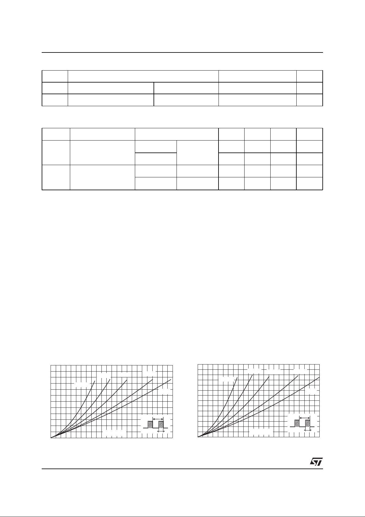
Fig. 1: Average forward power dissipation versus
average forward current (1N5817/1N5818).
PF(av)(W)
0.6
0.5
0.4
0.3
0.2
0.1
0.0
0.0 0.1 0.2 0.3 0.4 0.5 0.6 0.7 0.8 0.9 1.0 1.1 1.2
δ = 0.05
δ = 0.1
δ = 0.2
IF(av) (A)
2/5
δ = 0.5
=tp/T
δ
δ = 1
T
tp
Fig. 2: Average forward power dissipation versus
average forward current (1N5819).
PF(av)(W)
0.7
0.6
0.5
0.4
0.3
0.2
0.1
0.0
0.0 0.1 0.2 0.3 0.4 0.5 0.6 0.7 0.8 0.9 1.0 1.1 1.2
δ = 0.05
δ = 0.1
δ = 0.2
IF(av) (A)
δ
δ = 0.5
=tp/T
δ = 1
T
tp

1N581x
Fig. 2-1: Average forward current versus ambient
temperature (δ=0.5) (1N5817/1N5818).
IF(av)(A)
1.2
Rth(j-a)=Rth(j-l)=45°C/W
1.0
0.8
Rth(j-a)=100°C/W
0.6
0.4
T
0.2
=tp/T
δ
0.0
0 25 50 75 100 125 150
tp
Tamb(°C)
Fig. 3-1: Non repetitive surge peak forward
current versus overload duration
(maximum values) (1N5817/1N5818).
IM(A)
10
9
8
7
6
5
4
3
I
M
2
1
0
1E-3 1E-2 1E-1 1E+0
t
δ
=0.5
t(s)
Ta=25°C
Ta=75°C
Ta=100°C
Fig. 2-2: Average forward current versus ambient
temperature (δ=0.5) (1N5819).
IF(av)(A)
1.2
1.0
0.8
Rth(j-a)=Rth(j-l)=45°C/W
Rth(j-a)=100°C/W
0.6
0.4
T
0.2
=tp/T
δ
0.0
0 25 50 75 100 125 150
tp
Tamb(°C)
Fig. 3-2: Non repetitive surge peak forward
current versus overload duration
(maximum values) ( 1N5819).
IM(A)
8
7
6
5
4
3
2
I
M
1
0
1E-3 1E-2 1E-1 1E+0
t
δ
=0.5
t(s)
Ta=25°C
Ta=75°C
Ta=100°C
Fig. 4: Relative variation of thermal impedance
junction to ambient versus pulse duration (epoxy
printed circuit board, e(Cu)=35mm, recomm ended
pad layout).
Zth(j-a)/Rth(j-a)
1.0
0.8
0.6
δ = 0.5
0.4
δ = 0.2
0.2
δ = 0.1
0.0
1E-1 1E+0 1E+1 1E+2 1E+3
Single pulse
tp(s)
δ
=tp/T
T
tp
Fig. 5: Junction capacitance versus reverse
voltage applied (typical values).
C(pF)
500
200
1N5817
100
50
1N5819
20
VR(V)
10
1 2 5 102040
F=1MHz
Tj=25°C
1N5818
3/5

1N581x
Fig. 6-1: Reverse leakage current versus reverse
volt age app lied (ty pica l valu es) (1N 5817/ 1N58 18).
IR(mA)
1E+1
1N5818
1E+0
Tj=125°C
1N5817
Tj=100°C
1E-1
1E-2
Tj=25°C
VR(V)
1E-3
0 5 10 15 20 25 30
Fig. 7-1: Forward voltage drop versus forward
current (typical values) (1N5817/1N5818).
IFM(A)
10.00
Fig. 6-2: Reverse leakage current versus reverse
voltage applied (typical values) (1N5819).
IR(mA)
1E+1
Tj=125°C
1E+0
Tj=100°C
1E-1
1E-2
Tj=25°C
1E-3
0 5 10 15 20 30 35 40
VR(V)
Fig. 7-2: Forward voltage drop versus forward
current (typical values) (1N5819).
IFM(A)
10.00
1.00
Tj=125°C
0.10
0.01
0.0 0.1 0.2 0.3 0.4 0.5 0.6 0.7 0.8 0.9
Tj=100°C
Tj=25°C
VFM(V)
Fig. 8: Non repetitive surge peak forward current
versus number of cycles.
IFSM(A)
30
25
20
15
10
5
Number of cycles
0
1 10 100 1000
F=50Hz
Tj initial=25°C
1.00
Tj=125°C
0.10
0.01
0.0 0.1 0.2 0.3 0.4 0.5 0.6 0.7 0.8 0.9 1.0 1.1
Tj=100°C
Tj=25°C
VFM(V)
4/5

PACKAGE ME CHANICAL D AT A
DO41 plastic
CA
O
/
D
C
O
/
D
BO
/
REF.
A 4 .1 5 .2 0.16 0.205
B 2 2.7 0.08 0.107
C 25.4 1
D 0.71 0.86 0.028 0.034
1N581x
DIMENSIONS
Millimeters Inches
Min. Max. Min. Max.
Ordering type Marking Package Weight Base qty Delivery mode
1N581x P art num ber
DO41 0.34g 2000 Ammopack
cathode ring
1N581xRL Part number
DO41 0.34g 5000 Tape & reel
cathode ring
Epoxy meets UL94,V0
Information furnished is believed to be accurate and reliable. However, STMicroelectronics assumes no responsibility for the consequences of
use of such information nor for any infringement of patents or other rights of third parties which may result from its use. No license is granted by
implication or otherwi se un der any pat ent or patent rights of STMic roelec tronics. S pecifications ment ioned in t his publ ication are subject to
change without notice. This publication supersedes and replaces all information previously supplied.
STMicroelectronics products are not authorized for use as critical components in life support devices or systems wi thou t ex press written approval of STMicroelectronics.
The ST logo is a registered trademark of STMicroe lectronics
© 1999 STMicroelectronics - Printed in Italy - All rights reser ved.
STMicroelectronics GROUP OF COMPANIES
Australia - Brazil - China - Finland - France - Germany - Hong Kong - India - Italy - Japan - Malaysia
Malta - Morocco - Singapore - Spain - Sweden - Switzerland - United Kingdom - U.S.A.
http://www.st.com
5/5
 Loading...