

Page 1
AND ALPHANUMERIC CONTROLLER
.
FULLY PROGRAMMABLE TIMING GENERATOR
.
ALPHANUMERIC AND GRAPHIC DRAWING
CAPABILITY
.
EASY TO USE AND POWERFUL COMMAND
SET:
- VECTOR, ARC, CIRCLE WITH DOT OR
PEN CONCEPT AND PROGRAMMABLE
LINE STYLE,
- FLEXIBLE AREA FILL COMMAND WITH
TILING PATTERN,
- VERYFASTBLOCK MOVE OPERATION,
- CHARACTER DRAWING COMMAND, ANY
SIZEAND FONTS AVAILABLE
.
LARGE FRAME BUFFER ADDRESSING
SPACE(8 megabytes) UP TO 16 PLANES OF
2048 x 2048
.
UP TO 256 COLORCAPABILITIES
.
MASK BIT PLANES FOR GENERAL CLIPPING PURPOSE
.
FRAME BUFFER CAN BE BUILT WITH
STANDARD 64 K OR 256 KDRAM OR DUALPORT-MEMORIES(video-RAM)
.
EXTERNAL SYNCHRONIZATION CAPABILITY
.
ON CHIP VIDEO SHIFT REGISTERS FOR
DOTRATE UPTO 18 MEGADOTS/S
.
8 OR 16-BIT BUS INTERFACE COMPATIBLE
WITH MARKET STANDARD MICROPROCESSORS
.
HMOS2 TECHNOLOGY
.
68 - PINPLCC PACKAGE
.
FOR DETAILED INFORMATION, REFER TO
TS68483USER’S MANUAL
DESCRIPTION
The TS68483 isan advancedcolor graphic processor that drastically reduces the CPU software
overhead for allgraphic tasks in medium and high
range graphic applications such as business and
personal computer, industrial monitoring system
and CAD systems.
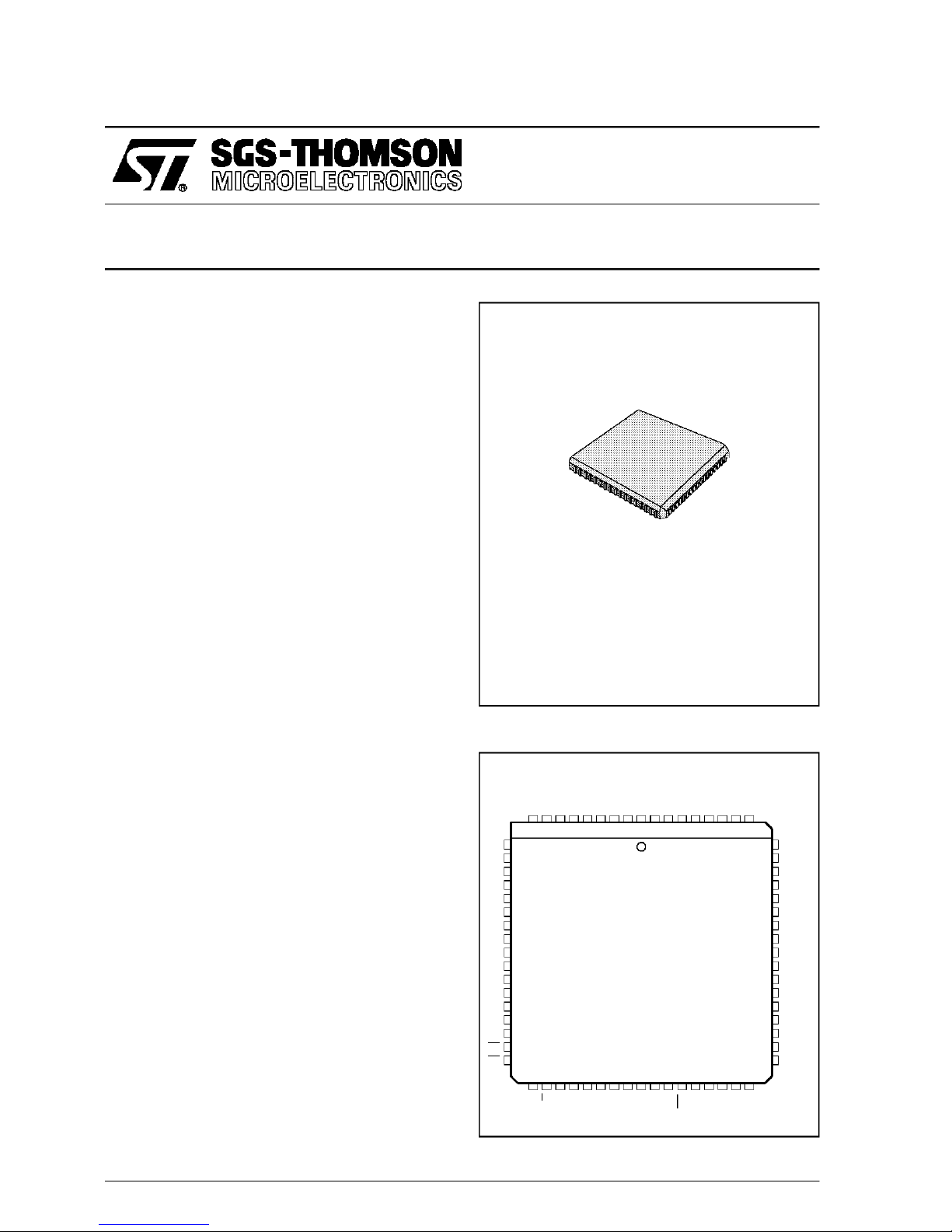
TS68483A
HMOS2 ADVANCED GRAPHIC
PLCC68
(Plastic Chip Carrier)
ORDER CODE : TS68483A
PIN CONNECTIONS
CYF1
D10
D11
D12
Vss
D13
D14
D15
CYF0
D3D2D1D0PC/HS
987654321
10
D4
11
D5
12
D6
13
D7
14
D8
15
D9
16
17
18
19
NC
20
NC
21
22
23
24
CS
25
26
DS
272928
NC
R/W
AE
SYNC IN
HVS/VS
BLK
686667
30313233343536373839404142
A1
A2
A3
A4
A5
A6
A7
B0
B1
A0
IRQ
Y2
Y1NCY0
CYS
6564636261
P1P2P3
P0
60
59
58
57
56
55
54
53
52
51
50
49
48
47
46
45
44
43
CLK
ADM15
ADM14
ADM13
ADM12
ADM11
ADM10
ADM9
ADM8
Vcc
ADM7
ADM6
ADM5
ADM4
ADM3
ADM2
ADM1
ADM0
68483-01.EPS
September 1993
1/30
Page 2
TS68483A
PIN DESCRIPTION
Name Type Function Description
MICROPROCESSOR INTERFACE
D (0 : 15) I/O Data Bus These sixteen bidirectional pins provide communication with either an 8
A (0 : 7) I Address Bus These eigth pins select the internal register to be accessed. The
AE I Address Enable When TS68483 is connected to a non-multiplexed microprocessor bus,
DS I Data Strobe Active Low
R/W I Read/Write - In non-multiplexed bus mode, this signal controls the direction of
CS I Chip Select This input selects the TS68483 registers for the current buscycle. A
IRQ O Interrupt Request This active-lowopen drain output acts to interrupt the microprocessor.
MEMORY INTERFACE
ADM
I/O Address/Data Memory These multiplexed pins act as address and data bus for display
(0 : 15)
CYS O Memory Cycle Start The falling edge of this output indicates the beginning of a memory
Y (0 : 2) O Memory Address These outputs provide the least significant bits of the Y logical address.
B (0 : 1) O Bank Number These outputs provide the number of the memory bank to be accessed
CYF (0 : 1) O Memory Cycle Status These outputs indicate the nature of thecurrent memory cycle (Read,
VIDEO INTERFACE
P (0 : 3) O Video Shift Register
Outputs
PC/HS O Phase Comparator/
Horizontal Sync.
HVS/VS O Composite or Vertical
Sync.
SYNC IN I External Sync Input This input receives an external composite sync. signal to synchronize
BLK O Blanking This output provides the blanking interval information.
OTHER PINS
V
CC
V
SS
S Power Supply + 5 V Supply
S Ground Ground
CLK I Clock Clock Input
or 16-bit host microprocessor data bus.
address can be latched by AEfor direct connection to address/data
multiplexed microprocessor busses.
this input must be wired to VCC.
For directconnection to a multiplexed microprocessor bus, the falling
edge of AE latches the address on A (0 : 7)pins and the CS input. With
an Intel type microprocessor, AE is connected to the processor
Address Latch Enable (ALE)signal.
- In non-multiplexed bus mode, DS low enables the bidirectionnaldata
buffersand latches theA (0 : 7) lines on its high to low transition.
Data to be written are latched on the rising edge of this signal.
- In multiplexed bus mode, this signal low enables the output data
buffersduring a read cycle. With intel microprocessors, this pin is
connected to the RD signal.
dataflow through the bidirectional data buffers.
- In multiplexed bus mode, this signal low enables the input data
buffers. The entering data are latched on its risingedge. With Intel
microprocessors, this pin is connected to the WR signal.
low levelcorresponds to an asserted chip select.
In multiplexed mode, this input is strobed by AE.
memory interface.
cycle.
during the current memory cycle.
Write, Refresh, Display).
These four pins correspond to the outputs of the internal video shift
registers.
This output can be programmed to provide either the phase comparator
output or the horizontal sync. signal.
This output can be programmed to provide either the composite sync.
signal or the verticalsync. signal.
TS68483. This input must be grounded if not used.
68483-01.TBL
2/30
Page 3

BLOCK DIAGRAM
TS68483A
MICROPROCESSOR INTERFACE
AE, DS
R/W, CS
R0
R1
R2
R3
R12
V
52
CC
19
V
SS
R23
DRAWING
AND
ACCESS
PROCESSOR
D [0:15] A [0:7] IRQ
48
16
GENERATOR
R4
R10
VIDEO
TIMING
38
43
2
5
4
3
SYNC IN
ADDRESS
VIDEO
SHIFT
REGISTERS
DATA
32
21
DATA
32
CLK
BLK
PC/HS
HVS/VS
VIDEO
INTERFACE
P [0:3]
DISPLAY MEMORY LOGIC
65
CYS CYF [0:1] B [0:1] Y [0:2] ADM [0:15]
232
DISPLAYMEMORY INTERFACE
16
ABSOLUTEMAXIMUMRATINGS
Symbol Parameter Value Unit
V
CC*
V
in*
T
A
T
stg
P
Dm
* With respect to VSS.
Stresses above those hereby listed may cause permanent damage to the device. Theratings are stress ones only and functionaloperation of
the deviceattheseor anyconditions beyondthose indicatedin theoperational sections of thisspecificationsis not implied.Exposure to maximum
rating conditions for extended periods may affect device reliability. Standard MOS circuits handling procedure should beused toavoid possible
damage to the device.
Supply Voltage – 0.3, 7.0 V
Input Voltage – 0.3, 7.0 V
Operating Temperature Range 0, 70 °C
Storage Temperature Range – 55, 150 °C
Max Power Dissipation 1.5 W
3/30
68483-02.EPS
68483-02.TBL
Page 4

TS68483A
ELECTRICALCHARACTERISTICS
= 5.0 V ± 5%,VSS=0, TA=TLto TH) (unless otherwisespecified)
(V
CC
Symbol Parameter Min. Typ. Max. Unit
V
CC
V
IL
V
IH
Iin Input Leakage Current 10 µA
V
OH
V
OL
P
D
C
in
I
TSI
Supply Voltage 4.75 5 5.25 V
Input Low Voltage – 0.3 0.8 V
Input High Voltage 2 V
Output HighVoltage (I
= – 500 µA) 2.4 V
Ioad
Output Low Voltage
= 4 mA ; ADM (0 : 15), I
I
Ioad
= 1 mA ; other Outputs
Ioad
CC
0.4 V
Power Dissipation 700 mW
Input Capacitance 15 pF
Three State (off state) InputCurrent 10 µA
V
68483-03.TBL
I - GENERALOPERATION
I.1 - Introduction
The TS68483 is an advanced color graphics controllerchip. It isdirectlycompatiblewithmostpopular8 or 16-bit microprocessors.
Itsdisplaymemory, containingtheframebufferand
the character generators,may be assembled from
standarddynamic RAM components.
On-chipvideo shift registersand fully programmable Video Timing Generator allow the TS68483 to
be used in a wide range of terminals or computer
design.
Additionalinformationonapplicationscan befound
in the TS68483User’s Manual.
I.2 - TypicalApplication BuildingBlocks
In atypical using TS68483,a hostprocessordrives
a display unit which drives in turn a color CRT
monitor.
The display unitconsists of four hardwarebuilding
blocks:
- an TS68483advanced graphics controller,
- a displaymemory (dynamic RAM),
- adisplaymemoryinterface,comprisinga fewTTL
parts,
- a CRTinterface of CRT drivers.
For enhanced graphics, the CRT interface may
include a color look-up table circuit. For high pixel
rate (over 18 Mpixels/s), the CRT interface must
includehigh speed video shift registers.
Thedisplaymemoryinterfaceand organizationare
discussedin full details in theUser’s Manual.
I.3 - TS68483 Functions
All the TS68483functionsare under the controlof
the host microprocessor via 24 directly accessible
16-bitregisters. These registers are referred to by
their decimalindex (R0-R23)(see Figure 1).
Figure1 : Register Map
15 087
R0
R1
R2
R3
R4
R5
R6
R7
R8
R9
R10
R11
R12
R13
R14
R15
R16
R17
R18
R19
R20
R21
R22
R23
Sx Sy
TEXLIN
XOR
H
DWX FPY
FPX BKX
DWY
CONF
STATUS
STOP
MODECOMMAND
MARGINCOLOR
YOR
BPY
BKY
dy dx
Yd
Xd
DYd
DXd
RAD
Ys
Xs
DYs
DXs
C0
C1
COMMAND,
DRAWING
ATTRIBUTES
VIDEO
TIMING
GENERATOR
SHORTRELATIVE
REGISTER
DESTINATION
POINTER
AUXILIARY
GEOMETRIC
ARGUMENTS
SOURCE
POINTER
I.3.1 - VIDEO TIMING AND DISPLAY PROCESSOR (R4 to R10).
Thevideo timing generatoris fully programmable:
anypopularhorizontalscanning period from 20 µs
to 64 µs may be freelycombinedwith any number
68483-03.EPS
4/30
Page 5

TS68483A
of lines per field (up to 1024). The address of the
displayviewport (this part ofthe displaymemory to
be actually displayed on the screen) is fully programmable. The display processor provides the
display dynamic RAM refresh (see video timing
generatorsection for details).
I.3.2 -DRAWING ANDACCESSCOMMANDS (R0
to R3, R12 to R23).
The 16 remaining registers are used to specify a
comprehensive set of commands. The highly orthogonal drawing command set allows the user to
”draw” in the displaymemory such basic patterns
as lines, arcs, polylines, polyarcs, rectangles and
characters. Efficient procedures are available for
either area filling and tiling or line drawing and
texturing.Lines may be drawnwith a PEN in order
to get thick strokes. Any drawing is specified in a
13x213
2
drawingcoordinate system.
Toaccessthe displaymemory, the hostmicroprocessor has an indirect, sequential access to any
”window”. Accesscommands can be used to load
the charactergeneratorsas well asto loador save
arbitrarywindows stored in the frame buffer.
I.4 - Data Type Definitions
PIXEL : this is the smallest color spot displayable
on theCRT.
PEL: a PictureElement is the codingof a PIXELin
the display memory. The TS68483 can handle 4
differentPEL formats :
- 4 colorbits - short
- 4 colorbits + 1 mask bit - short masked
- 8 colorbits - long
- 8 colorbits + 1 mask bit - long masked
DRAWING COORDINATES : (see Figure 2)
The drawing commands are specified and computedin a 2
drawing coordinates are clipped and mapped into
the 2
11x211
13x213
cyclical coordinatesystem.The
display memory addressing space.
Furtherclippingto the actualframe buffersizemay
be performedby the user designed memory interface.
DISPLAYMEMORY:
This is the dedicatedmemory to the display unit.
This memory is addressed as four banks of 4-bit
plane each.
BITPLANE :
Each bit planehasa maximumcapacityof2
11x211
bits. A byte wide organization of each bit plane is
required.
MEMORYADDRESS : (see Figure3).
In order to addressone bit in the display memory,
the user must specify :
- Abank number(2 bits)B = 0 to3
- Abit plane number (2 bits) Z = 0 to 3
- AY address (11bits) Y = 0 to 2047
- An X address (11bits) X = 0 to2047
MEMORYWORD : (see Figure 3)
A32-bitmemory word canbe either read or written
during each memory cycle (8 CLK periods), one
byte at a time in each bit plane in the addressed
bank. The memory bandwidth is in the 6 to 8Mbytes/srange.
VIEWPORT :
This is anyrectangulararray of pels located in the
displaymemory.
FRAMEBUFFER :
This is the biggest viewport which can be held in
the display memory. The frame buffer maps a
window at the origin of the drawingcoordinates. A
short pel frame buffer may be locatedin anybank.
Alongpel framebuffermustbe locatedinthe”bank
0, bank 1” pair.
DISPLAYVIEWPORT :
This is the viewportwhich is displayedon screen.
MASK BIT PLANE:
Whenmaskedpelsareused,amaskbitplanemust
be associated to a frame buffer. Mask bit planes
may be locatedin anyplane of bank 3.
CELL :
ACELLis anypatternstored inthedisplaymemory
asa rectangulararrayof bitmappedelements.The
drawing of any CELL may be specified with a
scalingfactor.
CHARACTER :
Thisis aone bitper elementCELL.It maybe stored
in anybit plane,then coloredand drawnin a frame
bufferby use of PRINTCHARACTER command.
OBJECT :
This is a one short pel per element CELL. It may
bedrawnorloadedinaframebuffer.Asourcemask
bit may be associated to each element. An OBJECT may then be printed in anotherlocation by
use of a PRINT OBJECTcommand.
PEN :
This is the patternwhich is repeatedlydrawnalong
the coordinatesdefinedby eithera LINEoran ARC
command.
The PEN may be a DOT (singlepel), a CHARACTERor an OBJECT.
5/30
Page 6
TS68483A
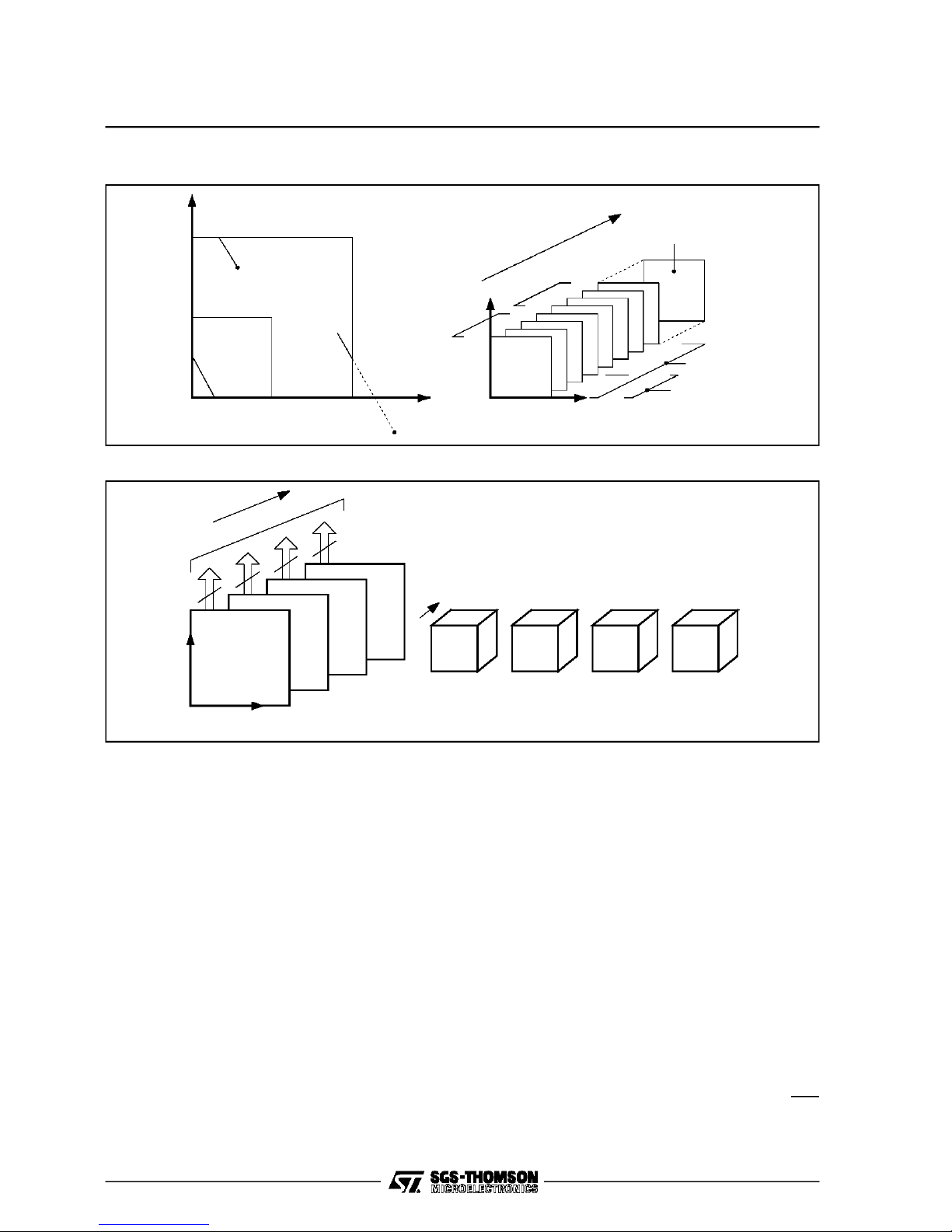
Figure2 : CyclicalDrawing Coordinates to Display Memory Mapping
Y
13
2
11
2
11
0
2
13
2
BANK 0
X
Figure3 : The DisplayMemory AddressingSpace
Z
32
8
8
8
8
2
1
XY0
7
3
BANK0 BANK 1 BANK 2 BANK3
Y
BANK 1
Z
4
3
2
1
0
X
BANK3
MASK
M
BITS
7
6
5
LONG PELS
SHORT PELS
68483-04.EPS
THE MEMORY WORD
II - COMMANDS
II.1 - Introduction
The command set is strongly organized in five
subsetor commandtypes.
DRAWING COMMANDS :
- LINEAR(line, arc)
- AREA(rectangle,trapezium, polygon, polyarc)
- PRINTCELL (print character,print object)
ACCESSCOMMANDS
CONTROLCOMMANDS (movecursor,abort)
The commandsare parametered ; this means that
anycommand can be executed with options freely
selected out of a given option set. This option set
is common for any command of a given type. For
example,any drawing command may be parametered for destinationmaskbit use.
The command code also defines the command
type and its parameters.A command iscompletely
defined when a valuehas been set for each of its
6/30
4 BANKS OF 4 BIT PLANES EACH
arguments.
These arguments are :
- the geometric arguments given in the drawing
coordinate system for every drawing command.
They are automaticallymapped into the destination framebuffer ;
- the parametric valuesare the values required by
the selectedparameters ;
- the attribute valuesare the other values required
by adrawing command ; colors or scaling factors
for example ;
- the display memory addresses.
The command code is specified in register R0.
Beforeinitiating a commandexecution,each argument must be specified in its dedicatedregister : an Xd, Yd drawing coordinate pair for example, is
always locatedin registers R14, R15.
The monitoringof acommandexecutionisdone by
reading the status register R12 or using the IRQ
signal.
68483-05.EPS
Page 7
Table1 : Command Set Structure
Command Drawing Mode Type Group
Line
Arc
Rectangle
Trapezium
Polygon
Polyarc
Print Char
Print Object
Load Viewport
Save Viewport
Modify Viewport
Move Cursor Abort Control
Up to the Pen Linear
Monochrome Area
Bichrome
Polychrome
Cell
Access
TS68483A
Drawing
Management
68483-04.TBL
II.2 - Pointers and GeometricArguments (see
Figure4)
Pointersare used to specify main geometric argumentsand display memory addresses.
II.2.1 - DISPLAYMEMORY ADDRESS
Abit in the displaymemory is addressedby :
- a banknumber B =0 to 3
- a plane number Z = 0 to 3
- an X address X = 0 to 2047
- a Y addres Y = 0 to 2047
II.2.2 - DESTINATIONPOINTER :
RegistersR14 to R17
This pointer gives the coordinate (Xd, Yd) and
dimension(DXd, DYd) of eithera lineor a window
in the drawingcoordinate system. These drawing
coordinates are easily mapped into a PEL DISPLAYMEMORYaddress.
(X, Y) coordinatesare clippedto 11bits in order to
get the Xd, Yd destination pel addresses.
A bank number Bd must be explicitly provided to
addressa destinationframebuffer.Whenlong pels
are used, Bd must be even.
Whenmasked pelsare used, the destinationmask
planenumber Zd(implicitly inbank 3) mustalsobe
provided.
II.2.3-SOURCEPOINTER:RegistersR20 toR23.
A source cell such as a character, a pen or an
object, is addressed by the source pointer in the
displaymemory.
Asource pointer specifies :
- a banknumber Bs = 0 to 3
- a Ysaddress Ys = 0 to 2047
- an Xsaddress; this addressis a byte addressso
thatthe 3 LSBs are not specified Xs = 0 to 255
- a celldimension DXs, DYs
- a bit plane address Zs.
Whena characteris addressed,Zsgivesthe plane
number into the bank Bs. When an object is addressed Zs gives the source mask plane number
in the bank B3.
II.2.4 - NOTES:
1. The TRAPEZIUM command makes a special
use of R21. In this case, R21 holds an X1
drawingcoordinatewhich has the same format
as Xd.
2. The ARC and POLYARC commands require
two extra geometric parameters (RAD and
STOP). They are specified in the drawing
coordinatessystemandstoredinregistersR18,
R19.
3. Anydrawingcommand may be parameteredto
use short incremental dimensions, DXY in
register R13 instead of the standard DXd, DYd
in the ”R16, R17” registerpair (see Figure 5).
4. The access commands use the destination
pointer location as a data buffer. The memory
add resses an d dimension of the ac cess
viewport are then specified in the source
pointer,independentlyof the data transfer.
5. DXd, DYd and DYs may specify a negative
value.In thiscase,theymust becodedbya sign
(0 = positive, 1 = negative) and an 11-bit
absolute value.
7/30
Page 8
TS68483A
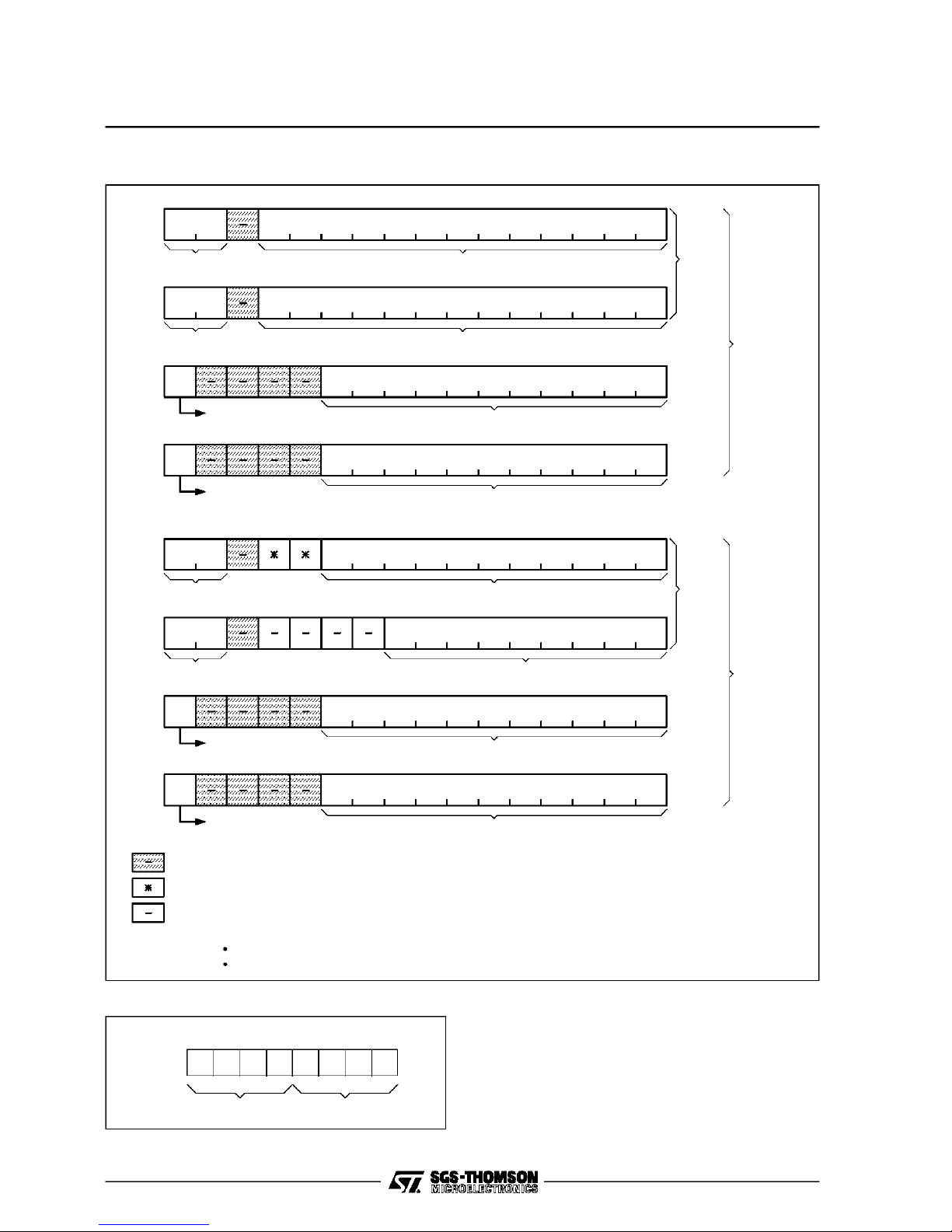
Figure4 : Pointers
1514131211109876 45 3210
R14
Bd
Yd
13-bit positive valueBank number
Pel
address
R15
R16
R17
R20
R21
Character cell plane (PCA)
or source mask plane (PVS, PVF)
R22
Zd
Plane number 13-bit positive value
S
Sign
S
Sign
Bs
Bank number
Zs
S
Sign
Xd
DYd
Absolute value
DXd
Absolute value
Ys
11-bit positive value
Xs
8-bit positive value
DYs
Absolute value
DESTINATION
POINTER
Byte
address
SOURCE
POINTER
U DXs
R23
Underlined (cell)
Reserved
Don’t care
Only used with TRAPEZIUM command
Note : Sign value
S = 0 positive
S = 1 negative + absolute value
Figure5 : Short DimensionRegister R13
76543210
SS
R13
dy dx
8/30
11-bit positive value
II.3 - DestinationMask and Source Mask
Amask bit may be associatedto any pel stored in
the display memory.
II.3.1 - DESTINATION MASK USE (DMU)
Any drawing command may be parametered for
destinationmask use.In thiscase, any destination
pel cannot be modified when its mask bit is reset.
68483-07.EPS
68483-06.EPS
Page 9
TS68483A
In other words :
- When the destination mask use (DMU) parameter isset :
- a pel may be modifiedwhen its mask bit is set
- a pel cannot be modified when its mask bit is
reset.
- When the destination mask use (DMU) parameter iscleared :
- a pel may be modified, independently of its
maskbit value.
This provides a very flexible clipping mechanism
not restricted to rectangularwindows. (See destination pointer section for destinationmask bit addressing).
II.3.2 - SOURCEMASK USE (SMU)
APRINTOBJECTcommand maybe parametered
for sourcemaskuse. In thiscase, thesource mask
bit associated with any source pel is read first.
When its mask bit is cleared, a source pel is consideredas transparent.(Seesourcepointersection
for source mask bit addressing).
In other words :
- When the SMU parameter is set, the color ofa
destination pel, mapped by a given source pel,
may take this source color value only when this
sourcebit maskis set. The destinationpel keeps
its own color value when the source bit mask is
cleared.
- When the SMU parameter is cleared, a source
pel color may be mapped into destination pel
color independentlyof the sourcebit mask value.
The source bit mask acts as a TRANSPARENCY/OPACITYflag which is enabled by SMU.A
PRINTOBJECT command may be independently
parameteredbybothSMUandDMU.Thisprovides
a very powerfultiling, print object or move mechanism.
II.4 - DrawingAttributes
Figure6 : Color Register
01234567
ODD
BANK
EVEN
BANK
The general drawing attributes are the colors, the
drawingmode, and the scalingfactor.
II.4.1.COLORS : RegistersR1 andR2
Two 8-bit color values, C0 and C1, may be speci-
fied in registers R1 and R2. The low order 4-bit
nibble of a color value is drawn in an even bank.
Thehighordercolornibbleisdrawninanoddbank.
When long pels are used, banks 0 and 1 are
generally addressed as the frame buffer. When
short pels are used, any bank may hold a frame
buffer.In thiscase, thebankparityselectsthe color
nibble used. (See destination pointer section for
bankaddressing).
II.4.2.DRAWINGMODE : RegisterR0
The drawing mode defines the transforms to be
applied to the pels designated by the drawing
commands. There are threedrawing modes.
II.4.3.MONOCHROME MODE
Any AREA drawing command, RECTANGLE for
instance,defines through its geometricarguments
anactive set of destinationpels, that is to saya set
ofpels to be modified.
When DMU = 1, this active set is further reduced
by the masking mechanism to only these destinationpels with a bit mask set.
The active destination pels are then modified accordingto two elementarytransforms codedin R0.
COLORTRANSFORM:
The color value C of each active pel is modified
according to one color transform selected out of
four :
- 00 - printed in C0 : C ← C0
- 01 - printed in C1 : C ← C1
- 10 - printed in ”transparent”: C← C
- 11 - complemented: C← C
This yields to a reversiblemarker mode.
MASK BITTRANSFORM :
The destination mask bit of each active pel is
modifiedaccordingto onemask transformselected
out of four :
- 00 - reset bit mask : M ← 0
- 01 - set bit mask : M ← 1
- 10 - no modification: M ← M
- 11 - complementbit mask : M ← M
This scheme allows the color bits and the mask bit
ofany pelbelongingto theactiveset tobemodified
independently. The color transform is performed
first.
II.4.4 - BICHROMEMODE
APRINTCHARACTER commandismore complex
because it involves two different active sets :
FOREGROUND and BACK GROUND.
TheFOREGROUNDis that set of destinationpels
printedfrom set elements inthe charactercell.The
68483-08.EPS
BACKGROUND is made of all the remaining pels
belongingto the destinationwindow.
When DMU = 1, the FOREGROUND and BACK
GROUND are further reduced by the destination
masking mechanism(see Figure 8).
A bichromedrawingmodeis definedby 4 elementary and independent transforms (see Figure 7) :
- a color transform and a mask transform for the
FOREGROUND PELS
9/30
Page 10

TS68483A
- a color transform and a mask transform for the
BACKGROUND PELS
II4.5 - POLYCHROME MODE
A print object command defines a source window
throughthe source pointer :
When SMU = 0, any pel of this window is active,
mapped and clipped to the destination window
dimension.
When SMU = 1, only pels which have a source
mask bit set are active,mapped and clipped to the
destinationwindow dimension.
In both cases, when DMU = 1, the active source
pelsarefurtherreducedby thedestinationmasking
mechanism.
Bothmasktransformsmust beprogrammedat ”NO
MODIFICATION” for correct operations (see Figure 7).
II.4.6-THELINEARDRAWINGCOMMANDCASE
A LINE or ARC drawing command may be executed in any drawing mode depending on the
PEN.
When the pen is a DOT, this pel is printed at each
activecoordinateaccordingtomonochromemode.
Whenthe penis aCELL, thiscell isprinted at each
activecoordinate.In the bichrome mode when the
cell is a character, and in the polychrome mode
when the cell is an object.
For eachactive coordinates,the activedestination
Figure8 : Print Character Command
set is defined by the cell dimensions (DXs, DYs).
Note : when the cell is an object, SMU is not
programmable and is implicitly set. A calculated
coordinate is active when the rotated LSB linear
texturebit in (R3) is set.
Figure7 : DrawingMode Register R0
BACKGROUND FOREGROUND
01234567
REGISTERR0
←
00
:
C
COLOR
MASK
BACKGROUND FOREGROUND
01234567
XXXX
XXXXXXXX
10 10
01
10
11
00
01
10
11
Monochrome
Bichrome
Polychrome
C0
←
C
:
C1
C
←
:
C
:
C
C
←
←
0
M
:
←
1
M
:
M
M
←
:
M
M
:
←
68483-09.EPS
10/30
DESTINA TION WINDOW CHA RACTER CELL
YY
(Xd, Yd) (Xs, Ys)DXd > 0 DXs > 0
DYs < 0
DYd < 0
(Xd, Yd) (Xd, Yd)
DMU = 0 DMU = 1
MASK BIT =1
MASK BIT = 0
MAPPED CH ARA CTERWINDOW
MAPPED
CHARACTER
WINDOW
XX
NO MODIFICATION
FOREGROUND
BACKGROUND
YY
SET ELEMENT = 1
XX
ELEMENT =0
68483-10.EPS
Page 11

TS68483A
II.4.7- SCALINGFACTOR ANDCELLMAPPING:
(see Figures9 and 10)
Figure9 : ScalingFactor
15 14 13 12 11 10 9 8
R1
SX SY
SX or SY S
0
0
0
0
0
1
1
1
1
0
0
0
1
1
2
0
15
1
16
0
Any cell may be printed with a scalingfactor.
This scaling factor is an integer pair Sx, Sy = 1
to 16. This scaling factor is interpreted with the
Figure10 : Cell Mappingversus DYd, DYs SIGN
Y
Y
PRINT CHARACTER, PRINT OBJECT and LINEARcommands when the pen is a cell. The AREA
or ACCESS or LINEAR (DOT) commands are
neverscaled.
TheLINEAR (PEN)commandshouldbe used with
a scaling factor of 1 because the pen is clipped at
DXs,DYs.
Thescaling factor is first applied to the source cell
before mapping and drawing. The drawing and
mappingisprocessedwithsignbit of DYdandDYs
values (see Figure 10).
Notes:
- DXs is always positive
- The DYs sign mirrors the cell
- DXd must be positive with a PRINTCELL command
68483-11.EPS
- DXd and DYd may get any sign with a LINEAR
DRAWING command. If a pen is used, these
signsare then irrelevantto the pen drawing. The
pen is mapped with positive increment values.
Y
DXd > 0Xd, Yd
X
DYs > 0
Xs,Ys
DYs < 0
DYd < 0
DYd > 0
X
DXs > 0Xs,Ys
Y
DXs > 0
X
DYd > 0
DXd > 0Xd, Yd
Y
DXd > 0Xd, Yd
X
X
DYd < 0
Y
DXd > 0Xd, Yd
X
68483-12.EPS
11/30
Page 12

TS68483A
II.5 - CommandSet Overwiew
Figure11
PEN
Dyd
DXd
II.5.1 - LINEARDRAWING
LINE(Xd, Yd, DXd,DYd).ARC(Xd,Yd, DXd,DYd,
RAD, STOP).
The curvemay bedrawnwithany penandwith any
linear texture (register R3). For each set of computed coordinates,R3 is right rotated and the pen
is printed when the shifted bit is set.
II.5.2 - AREADRAWING
- RECT (Xd, Yd, DXd, DYd)
- TRAPEZIUM(Xd, Yd, DXd, DYd, X1)
- POLYGON(Xd, Yd, DXd, DYd)
- POLYARC(Xd, Yd, DXd, DYd, RAD, STOP)
EitherRECTorTRAPEZIUMallowstodrawdirectly
all the pels inside the boundary.
Any other closed boundaries may be filled by a
3-step process :
1. The mask bits inside a boundary box must be
reset by a RECTcommand.
2. AsequenceofmixedPOLYGONandPOLYARC
commandsdescribingtheclosedboundarysets
the mask bits of the pels inside this boundary.
3. This area may then be painted by a
RECTANGLEcommanddefinedfor abounding
box, with destination masking. It may also be
tiledby use of a PRINT CELL command.
Note : themask bitof anypel lying ontheboundary
itself is not guaranteedto be set by step 2.
II.5.3 - PRINTCELL COMMANDS
PRINT CELL (Xd, Yd, DXd, DYd ; Xs, Ys, DXs,
DYs).
The cell addressedby Xs, Ys, DXs, DYs is scaled
then printed at location Xd, Yd and clipped at the
dXd, dYd dimensions.
When dXd, dYd is muchlarger than DXs,DYs the
commandmay be parameteredforrepeatdrawing.
These commands may also be parametered for
destinationmask use.
Further more the PRINT OBJECT command may
be parametered for source mask use.
These commands have a wide range of applications : text drawing, area tiling, print or move objects, scale and move viewports.
Note : an underlinedcell is drawn when the MSB
ofR23 is set.
II.5.4 - ACCESSCOMMANDS
- LOAD VIEWPORT(Xs, Ys, DXs, DYs)
- SAVE VIEWPORT(Xs, Ys, DXs, DYs)
- MODIFY VIEWPORT(Xs, Ys, DXs,DYs)
These commands provide sequential access to a
viewportin a frame buffer fromthe microprocessor
database.
68483-12.EPS
Data are transferred to/from the display memory,
wordsequentially.
TheR14 to R17registers are used as a two memory word FIFO (memory wordis 8 short pels, i.e. 4
bytes).
The source pointer (R20-R23) is used to address
the viewport for all accesscommands.
When long pels are used, the command must be
executedonce morewhenthe banknumberin R20
hasbeen updated.
II.5.5 - COMMANDEXECUTION
Each on-chip 16-bit register has four addresses.
One address is used for plain read or write. The
otheraddressesare usedto initiatecommandexecution automatically on completion of the register
access.
This scheme allows the command code and its
arguments to be loaded or modified in anyother.
An incremental line drawing command, for example,maybe executedagainand againwithsuccessiveincrementaldimensions and whithout need to
reload the commandcode itself.
As soon as a command execution is started, the
FREEbit is clearedin the STATUSregister. Thisbit
is automatically set when the execution is completed.
Thecommandsaregenerallyexecutedonlyduring
retrace intervals. However full time execution is
possible when either the display is disabled or
videoRAM componentsare used.
II.5.6 - STATUS REGISTER(see Figure12)
This register holds four read-onlystatus bits :
- FREE : this status bit is set whenno execution is
pending
- VS : verticalsynchronizationstate
- SEM: thisstatusbit isset whentheFIFOmemory
wordis inacessible to the microprocessorduring
a viewporttransfer
- NSEM : this status bit is set when the FIFO
memorywordis accessible tothe microprocessor
during a viewport transfer.
Eachof thesestatusbits is maskable.Themasked
status bits are NORed to the IRQ output pin.
12/30
Page 13

TS68483A
Figure12 : StatusRegister
15 14 13 12 11 10 9 8
STATUSREGISTERR12
MASKNSEM
NSEM
MASKSEM
SEM
MASKVS
VS
MASKFREE
FREE
15 14 13 12 11 10 9 8 R12
IRQ
READONLY
III - MICROPROCESSORINTERFACE
III.1 - Introduction
The TS68483is directlycompatible withany popu-
Figure13 : On-chipAddress and Byte Packing
lar8 or 16-bithostmicroprocessor; eitherMotorola
type (6809, 68008, 68000) or Intel type (8088,
8086).
Thehost microprocessorhas direct access to any
of the twenty four 16-bit on-chip registers through
the microprocessor interfacepins :
- D(0:15) : 16 bidirectionaldata pins.
- A(0:7) : 8 address inputs
- AE, DS, R/ W, CS : 4 controlinputs.
The twenty four registers are mapped in the host
addressing space as 256 byte addresses (see
Figure13)
- A(1:5) select oneout of 24 registers.
- A0 selectsthe low orderbyte (A0 = 1) or thehigh
orderbyte (A0 = 0) of the selectedregister.
- A(6:7) providethe commandexecutioncondition.
The host microprocessor bus may be either 8 or
16-bits wide and may be address/datamultiplexed
68483-14.EPS
or not.
ThetwoflagsMBandBWinthe CONFIGURATION
register R10 allow the data bus size and multiplexed/non-mutiplexed organization to be specified(see Table2).
15 14 13 12 11 10 9 8 7 6 5 4 3 2 1 0
Table2 : MPU Selection
Type of MPU Bus
NonM ux
Mux
16-bit (68000) 0 0 1 UDS or LDS R/W O A (1 : 7) D (8 : 15)
8-bit (68008) 1 0 1 DS R/W AO A (1 : 7) D (0: 7)
16-bit (8086) 0 1 ALE RD WR O AD (1 :7) AD (8 : 15)
8-bit (8088) 1 1 ALE RD WR ADO AD (1 : 7) AD (0 : 7)
A7 A6 A5 A4 A3 A2 A1 A0
High/Low Byte Address
16-bit Register ADDRESS
Execution Condition
Byte Addressing
A0 = 0 A0 = 1
Conf. Reg. TS68483 Pins
BW MB AE DS R/W AO A (1 : 7) D (8 : 15)
68483-15.EPS
68483-05.TBL
13/30
Page 14

TS68483A
Figure14 : Interfacewith TS68000/68008MPU
TS68483TS68000
D [8:15]
29D [8:15]
V
CC
D [0:7]
A [1:7] A [1:7]
D [0:7]
A [1:7] A [1:7]
Figure15 : Interfacewith 8086/8008 MPU
88
AD [0:7]
D [0:7]
37 26
TS68483TS68008
D [8:15]
D [0:7]
8
D [8:15]
D [0:7]
7
A [1:7]
A [1:7]
37
25
28
29
25
28
26
CS
R/W
UDSor LDS
V
CC
CS
R/W
DS
68483-16.EPS
TS684838086
29AD[8:15]
25
26
28
ALE
CS
RD
WR
AD [0:7]
14/30
AD0
D [8:15]
D [0:7]
A [1:7]
37
TS684838088
29
25
26
28
ALE
CS
RD
WR
68483-17.EPS
8
88
7
Page 15

TS68483A
III.2 - HardwareRecommendations
(see Figures21, 22, 23 and 24)
A0-PIN :
1. Whenusing a 16-bit data bus, the A0input pin
must be grounded. No single byte access can
be performed.
2. In order to conform with the high byte/low byte
on-chip packing, the A0 input pin must be
inverted when using an 8-bit bus Intel type
microprocessor(8088 for example).
A(1:7),D(0:7), D(8:15) pins :
1. Withany 8-bit data bus, the D(0:7)and D(8:15)
pinsmust be paired in orderto demultiplex the
low order data bytes and the high order data
bytes.
2. Whenusing address/datamultiplexed bus, the
D(0:7) pins are paired with A(0:7) in order to
demultiplexdata from address.
AE, DS, R/ W, CS : See pin description.
III.3 - SOFTWARE RECOMMENDATIONS
1. The CONFIGURATION register R10 must be
first initialized.
The BW 15 flag is interpreted by the bus
interface to recognize an 8-bit/16-bitdata bus.
The MB and BW 15 flags are used to decide
when to initiate a commandexecution.
2. Each register byte has 4 addresses in the
microp rocessor memory map. These 4
addresses differ only by A(6:7). This scheme
allowsa 68008programmer to readorwrite any
data type (byte, word, long word) and
autom atically initi ate or not a command
executionat theendof thistransfer.Thetransfer
lasts one, twoor four bus cycles.
A68000 programmer isrestricted to onlyword and
long word data types (see Table 3).
Table3 : Command ExecutionCondition
Address
A7 A6 8-bit Data Bus 16-bit Data Bus
0 0 no Exec Any Type Any Type
0 1 Exec after aBus Cycle 1 Byte 1 Word
1 0 Exec After 2 Bus Cycles 1 Word 1 Long Word
1 1 Exec after 4 Bus Cycles 1 Long Word* ILLEGAL
Notes : Word transfer must respect word boundary.
Long word transfer must respect long word boundary.
* Not available with 8088 MPU type.
Execution Condition
Data Type Transfer
68483-06.TBL
IV - THE VIDEO TIMING GENERATOR RAM REFRESH AND DISPLAY PROCESS
IV.1 - Introduction
TheVideoTiming GeneratoriscompletelysynchronouswiththeCLKinput,whichprovidesa pixelshift
frequency(up to 18MHz). The Video TimingGenerator :
- delivers the blanking signal (BLK), the horizontal
(HS)and vertical(VS)synchronizationsignalson
respectiveoutput pins,
- schedulesthe memorytime allocated to the display process, dynamic RAM refresh and commandexecution,
- is fully programmable
- can be synchronizedwith an external composite
video sync signal connected to the SYNC IN
input.
IV.2 - ScanParameters (see Table 4 and Figure26)
IV.2.1 - TIMINGUNITS
The time unit of any vertical parameteris the scan
line.
The time unit of any horizontal parameter is the
memorycycle, which is 8 periodsof the CLK input
signal.
Thesetwo parametersare internallyprogrammed:
- Horizontal sync pulse duration= 7 cycles
- Verticalsync pulseduration = 2.5 lines.
IV.2.2- BLANKINGINTERVAL
The blanking interval starts :
- at the leading edge of the vertical sync pulse.
Vertical blanking interval actual duration is 2.5
lines more than the programmed value.
- two cyclesbeforethe leadingedgeof thehorizontal sync pulse. The actual horizontal blanking
interval duration is 3 cycles more than the programmedvalue.
Note : During the programmed blanking interval,
the video output pins P(0:3) are forced low.
IV.2.3- PORCHAND MARGINCOLOR
During the porch interval, the programmablemargin coloris displayedon the P(0:3) outputs.
The display process may be disabled by setting
DPD flag.Thiswill beinterpretedas a porchextension.
Note : By process, the value of the block porch
must be strictlyabove 0.
15/30
Page 16

TS68483A
IV.2.4. MEMORYTIME SHARING(see Figure 16)
Figure16 : VideoProgramming
HORIZONTAL
Horizontal Minimum
Number of Cycles
BKX
FFX
DWX
H
BLKX
4
3
3
19
7TTL
1T2T
3T BKX
BLANKING
FPX
FRONT
PORCH DWXDISPLAY
MARGIN
The Video Timing Generator allocates memory
cycles to either the display process, RAM refresh
or command execution. In this respect, the scan
lines perfield are split between: the DWYdisplayable lines.
WhenVRE = 0, Video RAMs are not used.
The DWY x DWX cyclesin the display intervalare
allocatedto the display process when it is enabled
(DPD = 0). When the display process is disabled,
these cycles are allocated as for non displayable
lines.
When VRE = 1, one cycle per displayline is allocated to the display process. Other cycles are
allocated as for non displayable lines. The last
periodof theBLKX signal may be used to load the
internal video RAM shift register.
- the non displayablelines. In one out of nine non
displayablelines,DWXcyclesare allocatedtothe
refreshprocess when it is enabled (RFD = 0).
- In Float cycle, an external X address must be
provided. The Y address is still provided on
16/30
2H
DISPLAY
BACK
PORCH
FRONT
PORCH
FPY
DISPLAY
DWY
BACK
PORCH
= BPY - 25
25 Lines
BLANKING
Vertical Minimum
Numberof Lines
BKY
FPY
DWY
BPY
BKY
BLKY
1
1
3
1
ADM(0:7)and Y(0:2),whileADM(8:15)areinhigh
impedancestate.
IV.2.5.COMMANDACCESS RATIO
This allocation scheme leaves about 50% of the
memory bandwidth for command access when
programminga standard TV scan.This ratio drops
to the 30% range when a better monitor is in use
(32µsoutof43µsdisplayableperline,360lines out
of 390 fora 60Hz field rate). The higherresolution
means more memory accesses in order to edit a
given percentage of the screen area. In this case
Video RAMs are very helpful to keep 90% of the
memorybandwidthavailableforcommandaccess.
IV.3- Display Process
The Video Timing Generator allocates memory
cyclestothe DisplayProcessorin orderto readthe
Display Viewport from memory. The Display Viewport upper left corner address is programmable
through DIB, YOR and XOR. The display viewport
dimensions are related to the display interval of
DWYlines by DWX cycles per field.
68483-18.EPS
Page 17

TS68483A
IV.3.1 - YADDRESSES
WhenINE = 0, the fieldsare not interlaced. The Y
DisplayViewportaddress is initializedwith YOR at
the first displayable line thendecremented by 1 at
each scanline. The Display Viewportis thusDWY
pel high.
When INE = 1, the fields are interlaced. The Y
DisplayViewportaddress is initializedas shown in
the table below. It is then decremented by two at
each scan line. The viewport is thus 2 x DWY pel
high.
Even Field Odd Field
YorEven Yor Yor + 1
Yor Odd Yor – 1 Yor
Y display Viewport address initializationwhen INE = 1
IV.3.2 - X ADDRESSES AND MODXFLAGS
The X Display Viewport address is initialized with
XOR at the firstdisplayable cycle of eachdisplayableline.It isthenincrementedateachsubsequent
cycle accordingto MODX flags.
MODX1 MODX0 X INCR
0 0 + 1 Internal Read
0 1 + 1 External Dummy
1 0 + 2 External Dummy
1 1 External Float
Video Shift
Register
Memory
Cycle Type
Read
Read
In internal mode, the Display Viewport is 8. DWX
pel wide.The on-chip video shiftregisterare used.
InDummyread, thememoryisreadbut theon-chip
video shift registers are not loaded, instead they
retaintheir margincolor.External videoshift registersare presumed to be loadedby either 8 pelsor
16 pels per cycle according to the programmed
incrementvalue.
In Float cycle, an external X address must be
provided. The Y address is still provided on
ADM(0:7)and Y(0:2), whileADM(8:15)are in high
impedancestate.
Note : See Memory Organization and Memory
Timingfor further details on the memory cycles.
IV.3.3 - THE VIDEO RAM CASE (VRE = 1)
In thiscase, thelastcycleof thehorizontalblanking
interval is systematically allocated to the display
process for DWY scan lines per field.
This cycle bears the scan line address, the bank
numberand the X addresswhich is always XOR.
MODX must be programmed to use external shift
register(Dummy read).
IV.3.4- PANAND TILT
The host can tilt or pan the Display Viewport
throughtheframe bufferby modifyingYORor XOR
arguments.Panningisperformedon 8pel boundaries.
IV.4.DynamicRam Refresh
No memory cycles are explicity allocated to the
RAMrefreshwhen RFD = 1.
WhenVRE = 0 and DPD = 0, the Display Process
is supposed to be able to over-refresh dynamic
components.Thiscan be doneby carefullogical to
component address mapping. During the remaining non displayable lines, the Display Viewport
address continuesto be incremented : Y address
on eachline accordingto INE, X addressinitialized
by XOR then incremented according to MODX.
This Display viewport address is allowed to addressthe memoryfor DWX cyclesin onlyone line
out of nine for refresh purposes.
When VRE = 1 or DPD = 1, any line is processed
as anondisplayableline withrespectto therefresh
process.
IV.5.Configuration and ExternalSynchronization
The R10 register holds eight configurationflags.
Sixoftheseflags arededicatedto theVideoTiming
Generator.
- SSP : this flagselects the synchronizationoutput
pin configuration:
- NPC, NHVS, NBLK : these three flags invert the
PC/HS, HVS/VS and BLK outputs respectively.
(Ex. : WhenNBLK = 1 blanking is activehigh).
The SYNC IN input pin provides an externalcom-
posite synchronization signal input from which a
Vertical Sync In (VSI) signal is extracted. The
SYNC IN signal is sampled on-chip at CLK frequency.Its risingsampled edgeis comparedto the
leading edge of HS. A PC comparison signal is
externally available (see SSP and NPC flags).
VSIE: thisflag enablesVSIto resettheinternalline
count.
HSIE: thisflag enablesthe risingedgeof SYNCIN
to actdirectlyonthe VideoTimingGenerator.When
the leading edge of HS does not match at 1 clock
period a rising edge of SYNC IN, one extended
cycle is performed (nine clock periods instead of
eight).
Flag
SSP = 1 HS VS
SSP = 0 PC HVS
Output Pins
PC/HS HVS/VS
17/30
Page 18

TS68483A
Table4
Name
DWY 10 1 R9 Number of Display lines per Field
INE 1 R8 Interlace Enable when INE = 1
BKY 5 1 R8 Number of Lines in Vertical Blanking – 2.5
FPY 5 1 R7 Number of Lines in Vertical Front Porch
BPY 8 3 R6 Number of Lines in Vertical Back Porch + 2.5
H 6 19 R6 Number of Double Cycles per Line
FPX 4 3 R8 Number of Cycles in Horizontal Front Porch
BKX 4 4 R8 Number of Cycles in Horizontal Blanking – 3
DWX 7 3 R7 Number of Cycles of the Display Window
XOR 8 R4
YOR 11 R5
DIB 2 R4
MODX 2 R9 Selection of the X Addressing Mode
MC 4 R4 Margin Color
RFD 1 R7 RAM Refresh Disable when RFD = 1
DPD 1 R7 Display Process Disable when DPD = 1
VRE 1 R8 Video RAM Enable When VRE = 1
Note : one cycle = 8 periods ofCLK Clock
Number
of Bits
Mininmum
Values
Register Description Function
X, Y, and bank logical address in the display
memory of the display viewport upper left corner
Vertical
Scan
Horizontal
Scan
Display
Process
Memory
Time
Sharing
68483-07.TBL
V.MEMORY ORGANIZATION
V.1- Introduction
The display memory is logically organized as four
banks of 4-bit planes. Thus a bit address in the
displaymemory isgiven by the quadruplet :
- B = bank number,from 0 to 3
- Z = plane number, from 0 to 3
- X = bit address into the plane,from 0 to 2047
- Y = bit address into the plane, from 0 to 2047.
Inonememorycycle(8CLKperiods),thecontroller
can access a memory word. This 32-bit memory
word holds one byte from each plane in a given
bank. In order to address this memory word, the
controllersupplies :
- B(0:1) : binary value of the bank number
- X(3:10): binary value of the wordaddress
- Y(0:10): binary value of the wordaddress.
Z and X(0:2) arenot supplied. Theygive only a bit
addressin a memory word.
V.2- Memory Cycles
24 pins are dedicated to the memory interface.
- ADM(0:15) : these16 bidirectional pins are multiplexed three times during a memory cycle (see
Figure 25) :
TA : address period. Output of the X(3:11)
and Y(3:11)address
TO : evendata period. The even Z bytesare
eitherinput or output.
T1 : odd data period. The odd Z bytes are
eitherinput or output.
18/30
Y(0:2) : three LSB Y address output pins (non-
multiplexed)
B(0:1) : two bank address output pins (non-
multiplexed)
- CYS: Cyclestartstrobeoutput(non-multiplexed).
CYS is at CLK/8 frequency. ACYS pulse isdelivered only when a command, display or refresh
cycle is performed.
- CYF(0:1) : Two cycle status outputs (non-multiplexed).Four cycletypesare defined:Command
Read, Command Write, RAM Refresh, Display
Access.
Becauseseveraloptionsmay be selectedfor RAM
refreshand display accessby the MODX and VRE
flags (see Video Timing Section), there are more
than four memory cycle types (see Figure 25 and
Table5).
V.3- DisplayMemory Desing Overview
The display memory implementationis application
dependant.Thebasic parameters are :
- the number of pixels to be displayed Nx.Ny
- the number of bits per pel
- the vertical scanning frequency,which must be
pickedinthe 40Hzto 80Hzrange(noninterlaced)
or in the60Hz to 80Hz range (interlaced).
This yields a rough estimateof thepixel frequency.
When the pixel frequency is in the 15 to 18MHz
range and 4 bits per pixel or leastare required,the
on-chipvideoregistersandstandarddynamicRAM
componentsmay be used.Whenhigher pixelrates
Page 19

TS68483A
or up to 8 bits per pixel are required,the designer
- RADand CAD Enable signals to the Mapper.
must provide external shift registers. Video RAM
componentsmay also be considered.
In either case, the user must design :
- A memory block. This is the hardware memory
buildingblock. It includesthevideo shift registers
if on-chip VSR cannot be used.It implies a RAM
componentchoice.
- An Address Mapper,which maps the logical address into hardware address : block selection,
RowAddress (RAD),Column Address(CAD).
- Amemory cycle controller. This controller monitors the CYF and CYS output pins fromTS68483
and block addressfrom the Mapper. It provides :
- TheCLKsignaltothe TS68483and a shiftclock
SCLK when external video shift registers are
used
- RAS, CAS, OE, R/ W signals to the memory
blocks
V.3.1- FRAME BUFFER (see Table 6)
A byte wide organization of each bit plane is required. Obviously a bit plane must contain the
Display Viewport size. A straight organization implementsonly one bit plane per block.
It may be cost effective to implement several bit
planes per block. Two basic schemes may be
used :
- One block, one Z : several bit planes, belonging
to differentbanks, but addressedby the same Z,
share a given block. There is little time constraint
if any.
- Oneblock, twoZ : twobitplanes,belongingtothe
same bank share a given block. In thiscase, this
block must be accessed twice during a memory
cycle.Thiscanbe solvedbytwosuccessivepage
mode accesses.
Table 5 : Memory Cycle Types
Output Pins
CYF1 CYF0 1 0 TA TO T1
1 0 Command Read Y,X Z0,Z2 Z1,Z3 Read
1 1 Command Write Y,X Z0,Z2 Z1,Z3 Write
01
00
Refresh : dummy read cycle isperformed.
Function
Display
Refresh
Modx Flags Multiplexed ADM
0
0
0
1
1
0
1
1
Y,X
Y,X
Y,X
Y,Hi-Z
Z0,Z2 Z1,Z3
Cycle Type
Read
Dummy Read + 1
Dummy Read + 2
Float X
68483-08.TBL
Table 6 : Frame Buffer Organization
Typical Block Size 16 k x 8 32 k x 8 64 k x 8 256 k x 8
One Block-one Bit Planes 512 x 256 512 x 512 1024 x 512 2048 x 1024
One Block-two Bit Planes 256 x 256 512 x 256 512 x 512
COMPONENTS : 64K BITS : 16K x 4 or 64K x 1
256KBITS : 32K x 8,64K x 4,256K x 1
VIDEORAM : 64K x 1, 64K x 4
Table 7 : The MultiplexingScheme
HIGHER BYTES
ADMS Multiplexed Pins 15 14 13 12 11 10 9 8
TA : Address Period 10 X 3
T0 : Even Z Byte Period 7 Z = 2 0
T1 : Odd Z Byte Period 7 Z = 3 0
LOWER BYTES
ADMS Multiplexed Pins 7 6543210
TA : Address Period 10 Y 3
T0 : Even Z Byte Period 7 Z = 0 0
T1 : OddZ Byte Period 7 Z = 1 0
68483-09.TBL
68483-10.TBL
19/30
Page 20

TS68483A
Figure17 : One Block - One Z
B0
B1
B2
B3
Figure18 : One Block - Two Z
Figure19
ADM [8:15]
8
8 (T1) 8 (T0)
Z3 Z2
ADM [8:15]
88
Z3 Z2
ADM [0:7]
Z1 Z0
ADM [0:7]
8
8 (T1) 8 (T0)
Z1 Z0
(T0. T1) = Page mode
68483-19.EPS
68483-20.EPS
76543210
0
1
Z
2
3
X [0:2]
V.3.2- MASKINGPLANES
Maskingplanesareveryuseful forgeneralpurpose
areafillingorclipping.Itmay bepracticaltouseone
ortwo planessmallerthan thecolorbit planeif they
cyclically cover a frame buffer.
The maskingplanes must be in bank3.
V.3.3- OBJECTSAND CHARACTERS
Objects may be located in unused parts of the
framebuffer.
Charactergenerators can be implemented in any
planeof anybank. They can also be implemented
in ROM.In thiscase, plane Z = 1 or 3offer relaxed
A MEMORYWORD
68483-21.EPS
access timerequirements.
V.4- Examples
Figure20. gives the schematicfor a 512x 384non
interlacedapplication.A CLK signalin the 15 to 18
MHz range should produce a 50 to 60Hz refresh
rate. Theon-chip videoshift registersmaybe used
if nomore thanfour bits perpixelare required.One
64 K x 8 memory block may be implementedusing
either eight 64 K x 1 or two 64 K x 4 components.
One memory block holds two 512 x 384 color bit
planes.
20/30
Page 21

Figure20 : MemoryOrganization for 512 x 384Application
TS68483A
BANK 0
BANK 3
CYCLE
CONTROLLER
64K x 8 64Kx 8
Z1 Z1+ 2
BANK ENABLE
CAD0
ADSEL
RAS
CAS
OE
WE
512
ADM [8:15] ADM [0:7]
64K x 8 64K x 8
384
128
B [0:1] Y [0:2]
23
Y
X
DATA
Z1/Z3
64K x 8 MEMORY BLOCK
One Blockthrough Page Mode
SPAREDAREA
LATCH
MUX
8
MEMORY
ADDRESS
DATA
Z0/Z2
VI - TIMING DIAGRAM
VI.1 - MicroprocessorInterface
TS68483has an eight bit address bus and a sixteen bit data bus. Little externallogic is needed to adapt
buscontrol signalsfrom most of the common multiplexedor non-multiplexedbus microprocessors.
UNMUX MODE
MicroprocessorInterface Timing : A(0:7), D(0:15), AE,DS, CS, R/ W
=5.0V ± 5%, TA=TLto TH,CL=100pF on D(0:15)
V
CC
Referencelevels : V
Indent Number Parameter Min. Max. Unit
1 Address Set up Time from CS 0 ns
2 Data Strobe Width(high) 65 ns
3 AS Set up Time from CS 0 ns
4 Data Strobe Width-low (read cycle) 160 ns
5 Address Hold Time from DS 0 ns
6 Data Access time from CS (read cycle) 130 ns
7 DS Inactive to High Impedance State (read cycle) 10 80 ns
8 R/W Set up Time from DS 20 ns
9 DS Width-low (write cycle) 80 ns
10 CS Set up Time from DS Active (write Cycle) 0 ns
11 Data in Set up Time from DS active (write cycle) 10 ns
12 Data in Hold Time from DS Inactive (write cycle) 15 ns
= 0.8V and VIH=2V on all inputs,VOL= 0.4Vand VOH= 2.4Von all outputs
IL
68483-22.EPS
68483-11.TBL
21/30
Page 22

TS68483A
Figure21 : Read Cycle
A [0:7]
AS (MPU)
CS
DS
R/W
DATA OUT
D [0:15]
Figure22 : WriteCycle
15
3
3
2
4
678
68483-23.EPS
A [0:7]
AS (MPU)
CS
DS
R/W
DATA IN
D [0:15]
15
3
10
2
8
11 12
9
3
68483-24.EPS
22/30
Page 23

TS68483A
MUXMODE
MicroprocessorInterfaceTiming : A (0 : 7), D (0 : 15), AE, DS, CS, R/W
=5.0V ± 5%,TA=TLto TH,CL= 10 pF on D (0 : 15)
V
CC
ReferenceLevels : V
Indent Number Parameter Min. Max. Unit
1 AE Width High 90 ns
2 Address Set up Time to AE Inactive 55 ns
3 Address and CS Hold Time to AE Inactive 55 ns
4 CS Set up Time to AE Inactive 40 ns
5 DS and R/W High 150 ns
6 DS Width-low (read) 240 ns
7 R/W Width-low (write) 110 ns
8 Data Access Time From DS (read) 210 ns
9 Data in Set up time from R/W Inactive (write) 150 ns
10 DS Inactive to High Impedance State (read) 10 100 ns
11 Data in Hold Time from R/W Inactive (write) 30 ns
12 AE Inactive toDS Active 20 ns
13 AE Inactive to R/W Active 20 ns
14 DS Inactive to AE Active 10 ns
15 R/W Inactive to AE Active 10 ns
16 R/W Inactive to Next Address Valid 100 ns
17 DS Inactive to Next Address Active 100 ns
18 Data in Set up Time from R/W Active (fast write cycle) 10 ns
= 0.8Vand VIH=2V on All Inputs, VOL= 0.4Vand VOH= 2.4V on All Outputs
IL
68483-12.TBL
23/30
Page 24

TS68483A
Figure23 : Read Cycle
AE
CS
DS
1
5
43
12
6
14
R/W
A/D
Figure24 : WriteCycle
AE
CS
DS
R/W
A/D
FAST WRITE
17
2
1
5
2
316
A
43
13
3
A
A
810
D
OUT
7
15
911
D
IN
18
D
IN
11
68483-25.EPS
68483-26.EPS
24/30
Page 25

TS68483A
VI.2 - Memory Interface
ADM (0 : 15), B (0 : 1),CYF (0 : 1), Y (0 : 2), CYS
=5.0V ± 5%,TA=TLto TH, CLK Duty Cycle = 50 %, Period T
V
CC
ReferenceLevels : V
Indent Number Parameter Min. Max. Unit
1 TCLK Clock Period 55 166 ns
2 Memory Cycle Time (T = 8 X T
3 Output Delay Time from CLK 35 ns
4 Output Data HI-Z Time from CLK 35 ns
5 Output Hold Time from CLK 10 ns
6 Input Data Hold Time from CLK (read cycle) 6 ns
7 Input Data Set up Time from CLK (read cycle) 10 ns
8 Input Data HI-Z Time from CLK T
Note : All timing is referenced to the rising edge of CLK(see timing diagram 3).
Figure25 : Memory Interface
= 0.8V and VIH=2V,VOL= 0.4Vand VOH=2.4V
IL
)ns
CLK
CLK
ns
68483-13.TBL
1
CLK
CYS
B [0:1]
CYF [0:1]
Y [0:2]
ADM [0:15]
WRITE CYCLE
ADM [0:15]
READ CYCLE
ADM [0:15]
DUMMY READ CYCLE
DISPLAY
FLOATING
CYCLE
3
ADM [0:7]
ADM [8:15]
2
5
3
4
A (X, Y)
A (X, Y)
A (X, Y)
A (Y)
33
D (EVEN Z)
5
D (EVEN Z) D (ODD Z)
4
577
6
D(ODDZ)
6
8
4
8
68483-27.EPS
25/30
Page 26

TS68483A
VI.3 - Video Interface
P0, P1, P2, P3, BLK, HVS/VS, PC/HS
=5.0V ± 5%,TA=TLto TH, CLKduty cycle = 50%
V
CC
Referencelevels : V
Indent Number Parameter Min. Max. Unit
1 TCLK : CLK Period 55 166 ns
2 CLK High Pulse Width 23 ns
3 Output Delay from CLK Rising Edge 30 ns
4 CLK Low Pulse Width 23 ns
5 Output Hold Time 10 ns
Figure26 : Timing Diagram
= 0.8V and VIH=2V,VOL= 0.4V and VOH=2.4V,CL=50pF
IL
1
68483-14.TBL
CLK
2
P [0:3]
BLK
HVS/VS
PC/HS
Figure27 : SynchronizationSignal Outputs
HS
(NPC = 1)
BLKX
P [0:3]
VS
HVS
(NHVS = 1)
BLK
(NBLK = 1)
VS
HVS
(NHVS = 1)
BLK
(NBLK = 1)
7T 7T
1T2T
MARGIN MARGIN
25LINES 25LINES
EVEN FIELD : BKY + FPY + DWY + BPY LINES EVEN FIELD
25LINES 25LINES
ODD FIELD : BKY + FPY + DWY - BPY 12 LINES EVENFIELD
BKY FPY DWY BPY
4
35
2HT
DWXFPXBKX
BPYDWYFPYBKY
Horizontal Sync
Non Interlaced
Example :
BKY+FPY+DWY+BPY= 525
Interlaced
Example :
BKY+FPY+DWY+BPY
= 312 for 625 Lines
68483-28.EPS
68483-29.EPS
26/30
Page 27

VII - TABLES
VII.1 - Register Map andCommand Table
Figure28
15 14 13 12 11 10 9 8 7 6 5 4 3 2 1 0
COMMAND
XOR
DWX
MODX1
MODX0
STATUS
H BFY
DEST. POINTER
SOURCEPOINTER
R0
R1
R2
R3
R4
R5
R6
R7
R8
0
R9
R10
BW MB VSIE HSIE NBLK NHVS NPC
R11
R12
R13
R14
R15
R16
S
R17
S
R18
ACW
R19
XY QF1 QF0
R20
R21
R22
S
R23
U DXs
SX SY
FPX
Bd
Zd
Bs
Zs
TS68483A
MODE
Odd Bank Even Bank
Odd Bank Even Bank
TEXLIN
0 DIB1 DIB0 MARGIN COLOR
YOR
DPD
RFD
VRE
INEBKX
SYNC
SS
: Don’t care : Used or not, according to thecommand
DY
Yd
Xd
DYd
DXd
RAD
STOP
Ys
DYs
C0
C1
FPY
BKY
DWY
DX
Xs
68483-30.EPS
27/30
Page 28

TS68483A
VII.2.Command Table
Per
DOT
DOT
CELL
CELL
AREA
MEMORY
WORD
WORD
MEMORY
WORD
MEMORY
4T
LOOP
EXECUTIONTIME
END COMMAND
POINTERS
ARGUMENTS
CELL+ 4T
5T
5T
INIT
CURSORPOSITION
Xd + DXd Yd + DYd
Xd + DXd Yd + DYd
XXXX
R20 R21 R22 R23
XXXXXXXXXXXXX
XXXXXXXXXXXXXXX
XXXXXXXXXXXXXXXXX
XXXXXXXXXXXXXXXXX
R14 R15 R16 R17
XXXXXXXXXXX
XXX
XXXXXXXXX
XXXXX
XXXXX
R0 R1 R2 R3 R13 R18 R19
4T
10T
CELL + 10T
15T
15T
XF YF
XF YF
XXXXXXXXX
X
X
X
X
X
4T
(see Note 1)
10T
10T
10T
Yd + DYd
Yd + DYd
Yd + DYd
Xd
Xd + DXd
Xd + DXd
XXXXX
XXXXX
15T
XF YF
XX
YdYdYd
Xd + DXd
6T
4T
Xd + DXd
XXXXX
XXXXX
XXXXX
XXXXX
5T
2T2T2T
Xs Ys
Xd + DXd
XX
4T
10T
4T
3T
Xs Ys
Xs Ys
Xd Yd + DYd
X
XXX
1T
3T
Xd + DXd Yd
X
Xd + DXd Yd + DYd
X
X
1T
1T if DMU = 1
1T if SMU = 1
2T if long pen are used
In other words, pels with color value 0 are transparent.
- DXd, DYd and DYsare signed values.
Note : With PVFcommand, any pel withcolor differentfrom 0 has its source maskimplicity set and used.
- DXs is always positive.
- T = memory cycle = 8 CLK clock periods.
2T if mask printingis required.
- For execution time, add tothe short pel loop in the table:
Commandexecutionis performed only outof the display periods.
Note 1 : For FLL and FLA commands,add 4Tand 8T respectively per pel belonging to the boundary.
SRU
SRU
SRU
SRU
SRU
SRU
SPSPSPSPSP
DMU
PARAMETERS
43210
00
0
0
CODE
765
01000
DLI
MNEM
TYPE
DOTLINE
I
L
DMU
DMU
00
POL PEN
1
0
000
PLI
DAR
PENLINE
DOTARC
EPA
N
DMU
DMU
0
1
POL PEN
111
PAR
REC
PENARC
RECTANGLE
R
DRA
SP
DMU
0
1
010
TRA
TRAPEZIUM
ARE
W
01 SRUSPDMU
010
FLL
POLYGON
A
I
N
28/30
SRUSPDMU
SRUSPDMU
BEG
BEG
011
101
FLA
PCA
POLYARC
PRINTCHARACTER
CEL
G
SRUSPDMU
REP
100
100
PVS
PRINTOBJECT
1 SRUDMU
REP
SMU
101
PVF
L
0 1 SRUDMUREP
000XFT INC
111
111
LDV
SAV
LOADVIEWPORT
SAVEVIEWPORT
ACCESS
00XFT INC1
0 XFT INC10
111
110
RMV
UDM
MODIFYVIEWPORT
UP-DOWNMOVE
SRU10 0 DWN
SRU00LEF1
00000
11111
110
110
110
111
NOP
CDM
DIAGONALMOVE
NOOPERATION
BRT
ABORT
CONTROL
LRM
LEFT-RIGHTMOVE
CURSOR
DMU = 1 : Destinationmask use.
SP= 1 : Short pel ; long pel whenSP = 0.
Shortrelative register use (R13).
The pen is a single pel.
:::
SRU = 1
PEN=0
POL= 0 : the pen is thecharacter cell addressed by the source ponter.
POL= 1 : the pen is theobject associated witha source mask addressed by the source pointer.
PEN= 1
Initatea polygon or polyarc filling.
This parametershould be reset only when the second drawing is not identical to the first one(Ex : first polygon,the polyarc).
:
BEG = 1
The source pointeris not auto-incremented,Xdirectionfirst.
:
INC = 0
XFT= 1 : the source pointeris auto-incremented,X direction first.
:
INC = 1
XFT= 0 : the source pointeris auto-incrementedor auto-decremented,Ydirectionfirst.
The cell is stepped and repeatedthroughthe destination window.
When REP = 0,only onecell is printed.
:
REP= 1
The cursor is mved down (up if DWN= 0).
The source mask is used.
:::
SMU= 1
DWN = 1
The cursor is mved left (rightif LEF = 0).
LEFT= 1
68483-31.EPS
Page 29

Figure29 : TypicalApplication
TS68483A
HOST
MICROPROCESSOR
TS68483
CRT CONTROLLER
DISPLAYMEMORY
INTERFACE
DISPLAY
MEMORY
SYSTEM
MEMORY
8 OR 16 BITS
SYNC SYNC
4
CRT
INTERFACE
R
MONITOR
G
B
68483-32.EPS
29/30
Page 30

TS68483A
PACKAGE MECHANICAL DATA
68 PINS - PLASTICCHIP CARRIER
Dimensions
B
6168
60
53
52
51
363534
A
44
G (Seating Plane Coplanarity)
Fe
E
d2
d1
M1
M1
921
10
17
18
19
26
27 43
Millimeters Inches
Min. Typ. Max. Min. Typ. Max.
M
M
D
A 25.02 25.27 0.985 0.995
B 24.13 24.33 0.950 0.958
D 4.2 5.08 0.165 0.200
d1 2.54 0.100
d2 0.56 0.022
E 22.61 23.62 0.890 0.930
e 1.27 0.050
F 0.38 0.015
G 0.101 0.004
M 1.27 0.050
M1 1.14 0.045
PMPLCC68.EPS
PLCC68.TBL
Information furnishedis believed to be accurate and reliable. However, SGS-THOMSON Microelectronics assumes no responsibility
for the consequences of use of suchinformation nor for any infringement of patents or other rights of third parties which may result
from its use. No licence is granted by implication or otherwiseunder any patent or patent rights ofSGS-THOMSON Microelectronics.
Specifications mentioned in this publication are subject to change without notice. This publication supersedes and replaces all
information previously supplied. SGS-THOMSON Microelectronics products are not authorized for useas critical componentsin life
support devices or systems withoutexpress written approval of SGS-THOMSON Microelectronics.
1994 SGS-THOMSON Microelectronics - All Rights Reserved
Purchase of I
2
I
C Patent.Rights to use these components in a I2C system, is granted provided that the system conforms to
2
C Components of SGS-THOMSON Microelectronics, conveys a license under the Philips
the I
SGS-THOMSON Microelectronics GROUP OF COMPANIES
Australia - Brazil - China - France - Germany - Hong Kong - Italy -Japan - Korea - Malaysia - Malta - Morocco
The Netherlands - Singapore - Spain - Sweden - Switzerland -Taiwan - Thailand - United Kingdom - U.S.A.
30/30
2
C Standard Specifications as defined by Philips.
 Loading...