

Page 1
Service manual
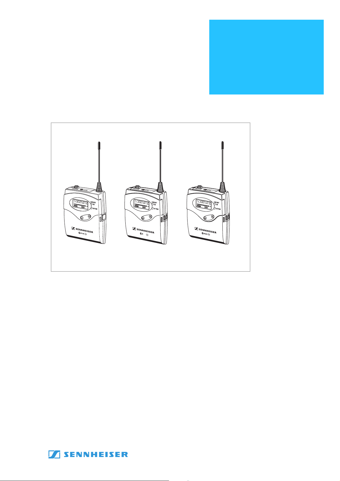
SK 100 G2
SK 300 G2
SK 500 G2
SA 280205
300
SK 100 G2 SK 300 G2 SK 500 G2
Short description
The SK x00 G2 bodypack transmitter has 8 channel banks with up to 20
preset channels (presets) and one freely adjustable frequency bank. With a
switching bandwidth of 36MHz 1440 frequencies can be selected in the
UHF band.
Features
• Pilot tone squelch for interference-free operation
• Mute function
• HDX compander system
• Charging contacts integrated in transmitter (does not apply to SK 100 G2)
• Backlighting of display with one keystroke
• Battery status display
• Robust metal housing
• Key-lock function
Subject to alterations
Sennheiser electronic GmbH & Co. KG • 30900 Wedemark
Phone: +49 (5130) 600 0 • Fax: +49 (5130) 600 300 1/27
Page 2

Safety requirements
Observe safety regulations.
Observe ESD instructions while handling electrostatically endangered components.
Only skilled persons are allowed to alter and repair. For repairs and exchanges only
approved components according to the current spare parts list are allowed.
For safety and certification reasons it is forbidden to alter the product without
authorisation. Otherwise, the person who has altered the product is liable for any
consequential damage.
repairs/exchanges The following instructions for overhaul and testing must be followed.
In case of unusual problems please contact your Sennheiser distributor.
For safety reasons unauthorised modifications and changes are not permitted.
SK 100 G2, SK 300 G2, SK 500 G2
2/27 02/2005
Page 3

Content
1 Controls and indicators..................................................................................4
2 Technical data.................................................................................................5
2.1 General.................................................................................................................... 5
2.2 AF characteristics.................................................................................................. 6
2.3 RF characteristics.................................................................................................. 7
3 Exploded view.................................................................................................8
4 Test and alignment instructions ............................................................... 10
4.1 Measuring and test equipment ....................................................................... 10
4.2 Measuring set-up................................................................................................ 10
4.3 Special service tools ........................................................................................... 11
4.4 Test table ............................................................................................................. 12
4.5 Reading out / Changing of device data via infrared adaptor.................... 15
5 Circuit diagrams........................................................................................... 17
Block diagram...................................................................................................................17
Mainboard, circuit diagram, part 1/3 .......................................................................... 18
Mainboard, circuit diagram, part 2/3 .......................................................................... 19
Mainboard, circuit diagram, part 3/3 .......................................................................... 20
RF board, circuit diagram, part 1/2..............................................................................21
RF board, circuit diagram, part 2/2..............................................................................22
Mainboard, interconnector assignment, part 1/2..................................................... 23
Mainboard, interconnector assignment, part 2/2..................................................... 24
RF board, interconnector assignment.......................................................................... 25
Mainboard, printed circuit board, solder side ............................................................26
Mainboard, printed circuit board, component side................................................... 26
RF board, printed circuit board, component side ...................................................... 27
RF board, printed circuit board, solder side................................................................27
SK 100 G2, SK 300 G2, SK 500 G2
02/2005 3/27
Page 4
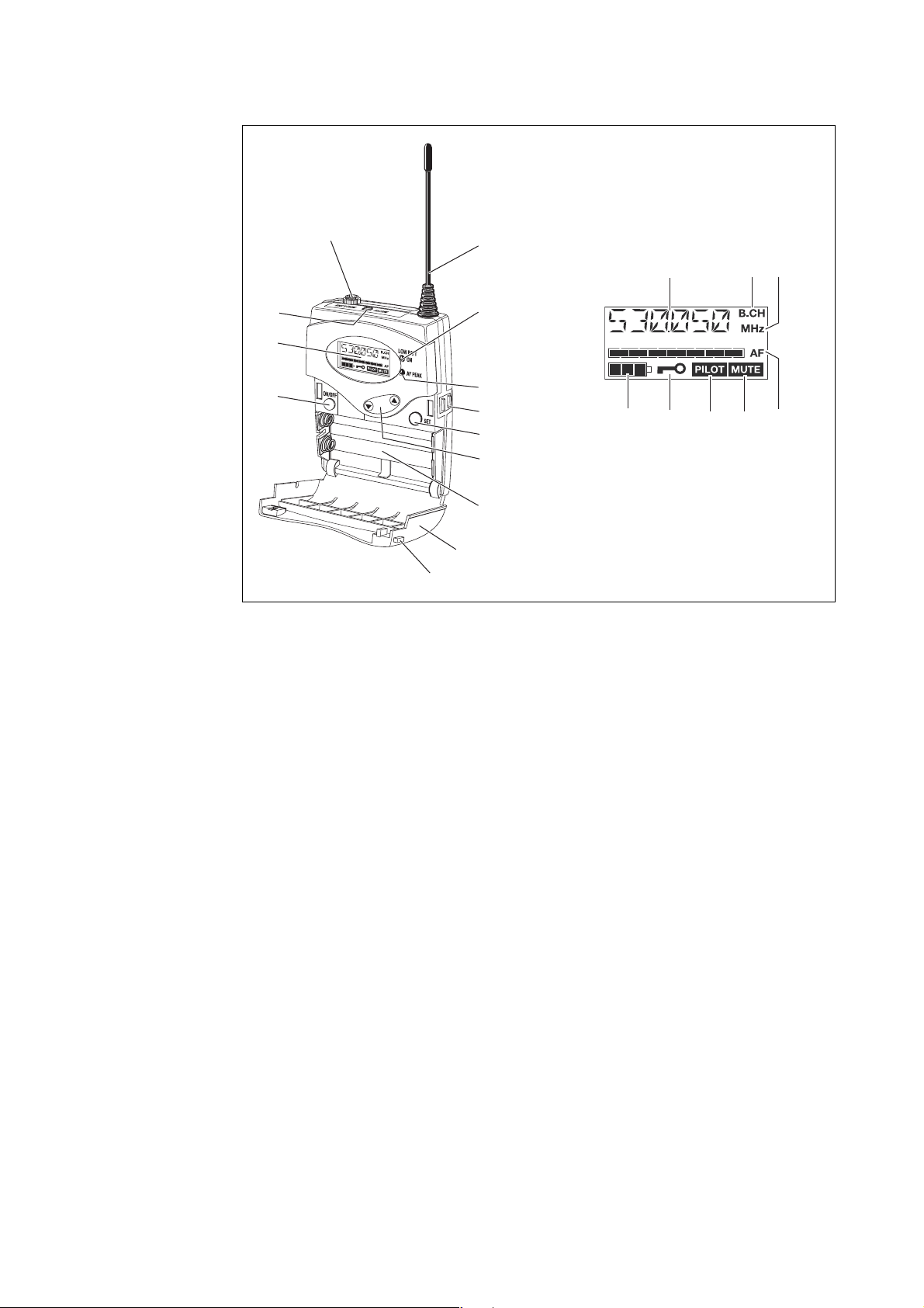
1 Controls and indicators
쐂
쐃
씈
쐉
쐈
쐅
Transmitter elements
쐎
쐇
쐋
쐏
쐄
쐆
쐊
쐃
Display elements
쐇
쐃 Microphone and line input
(MIC/LINE)
쐇 Antenna
쐋 Operation and battery status
indication, red LED (ON/LOW BAT)
쐏 Audio peak indication,
yellow LED (AF PEAK)
쐄 Charging contacts
(not SK 100 G2)
쐂 SET button (also save function)
쐆 / rocker button (UP/DOWN)
쐊 Battery compartment
쐎 Battery compartment cover
쐅 Unlocking button
쐈 ON/OFF button
쐉 LC display
씈 MUTE switch
쐃 Alphanumeric display of the
transmit frequency
쐇 Symbol for channel bank and
channel number
쐋 Frequency unit
쐏 7-step level display for audio
signal „AF“
쐄 „MUTE“ display (audio input is
muted)
쐂 „PILOT“ display (pilot tone
transmission is activated)
쐆 Lock mode icon (lock mode is
activated)
쐊 4-step battery status display
4/27 02/2005
SK 100 G2, SK 300 G2, SK 500 G2
Page 5

2 Technical data
2.1 General
Power supply voltage __________________ 2 batteries, type mignon AA; 1.5V
or battery pack BA 2015; 2.4V
Nominal voltage ______________________ +2.4V
Operating voltage _____________________ +1.8VDC to +3.1V
Switch-off threshold
when powered by batteries _________ +1.8V
when powered by BA 2015 accupack__ +2.0V
Switch-on threshold ___________________ +2.2V
Current consumption
at nominal voltage________________ ≤170mA
with transmitter switched off _______ ≤250µA
Operating time
when powered by batteries
or accupack _____________________ ≥8 hours
Battery status indication________________ 100%, 70%, 30%, low battery
Programming interface _________________ integrated infrared interface
Temperature range ____________________ -10°C to +55°C
Dimensions in mm_____________________ 82 x 63 x 23
Weight incl. batteries __________________ approx. 200g
Compliant with
Europe _________________________CE 0682
USA ___________________________FCC ID: DMOB2EUVL
Canada ________________________IC: 2099A-G2SK
Japan _________________________R202Y2378511; R202Y2378512;
R202B2378531; R202B2378532
DC
DC
DC
DC
DC
SK 100 G2, SK 300 G2, SK 500 G2
02/2005 5/27
Page 6

2.2 AF characteristics
Audio input LINE / MIC _________________ jack socket; 3.5mm
AF transmission range
Microphone_____________________ 40Hz to 18kHz (±3dB)
Japan: 40Hz to 15kHz (±3dB)
Line __________________________ 80Hz to 18kHz (±3dB)
Japan: 80Hz to 15kHz (±3dB)
AF sensitivity levels ___________________ 0 to -30dB
(also refer to input level on page 11)
Compander system ___________________ Sennheiser HDX
Preemphasis ________________________ HDX-dependent
Input impedance
Microphone_____________________ ≥10kW
Line __________________________ ≥ 1MW;
parallel 470pF, guitar-optimised
Total harmonic distortion
(at nominal deviation, 1kHz) ____________ ≤0.9%
Signal-to-noise ratio
(referring to peak deviation) ____________ 110dB(A) via HDX system
Max. input voltage (peak deviation)
Microphone_____________________ 1.8Veff (unw)
Line __________________________ 2.4Veff
SK 100 G2, SK 300 G2, SK 500 G2
6/27 02/2005
Page 7

2.3 RF characteristics
Modulation __________________________ Wideband FM, F8W
Number of transmission frequencies
(tunable in steps of 25kHz)______________ 1440
Frequency ranges in MHz _______________ 518-554
626-662
740-776
774-810 (Japan)
786-822
834-870
Number of frequency banks with
preset channels (presets)
SK 100 G2 ______________________ 8 banks with 4 channels each
SK 300 G2 ______________________ 8 banks with 8 channels each
SK 500 G2 ______________________ 8 banks with max. 20 channels
Freely adjustable frequency bank
(tunable in steps of 25kHz)
SK 100 G2 ______________________ 1 bank, 4 tunable channels
SK 300 G2 ______________________ 1 bank, 8 tunable channels
SK 500 G2 ______________________ 1 bank, 20 tunable channels
Switching bandwidth __________________ ≤36MHz
Harmonic emissions ___________________ ≤1µW
Spurious wave emissions
in the range from 47MHz to 862MHz__ ≤4nW
all other frequencies < 1GHz ________ ≤250nW
Channel grid _________________________ n x 25kHz
Frequency stability within temperature range ≤±10kHz
Intermodulation distance (±400 kHz)
at antenna distance ³10cm ______________ ≥36dB
Nominal deviation _____________________ ±24kHz
Peak deviation (at 1kHz) ±48kHz / Japan: <±40kHz
RF transmitting power max. at 50W _______ 30mW, +0.8dB/-3dB
Japan: 10mW, +0.8dB/-3dB
Covered bandwidth according to ETSI
at -20dBc_______________________ 140kHz
at -60dBc_______________________ 200kHz
Pilot tone
Frequency ______________________ 32.766kHz ±7.6Hz
Deviation _______________________ 2kHz ± 0.5kHz
Carrier signal-to-noise ratio referring to
peak deviation within switching
bandwidth___________________________ 75dB(A)
eff
SK 100 G2, SK 300 G2, SK 500 G2
02/2005 7/27
Page 8
3 Exploded view
003
002
002
001
011
023
017
018
002
002
010
022
022
012
(SK 100 G2)
002
016
008
008
(SK 300 G2,
SK 500 G2)
014
020
019
015
007
(SK 300 G2,
SK 500 G2)
019
007
(SK 100 G2)
004
005
013
006
009
SK 100 G2, SK 300 G2, SK 500 G2
8/27 02/2005
Page 9

Pos Description
001 Housing complete
002 Lens screw
003 Clamp
004 Cover, LCD
005 Cover, LOW BAT
006 Cover, infrared
007 SK 100 G2: plug right
SK 300 G2 / SK 500 G2: double charging contact
008 SK 100 G2: plug left
SK 300 G2 / SK 500 G2: single charging contact
009 Battery cover
010 Axle
011 Antenna
012 PCB RF
013 Battery case
014 PCB mainboard
015 LC display complet
016 Flat cable, 20 pin
017 Slide button, black
018 Rocker switch, black
019 Knob
020 Shielding cup
021 Label
022 Lens screw
023 Slottet nut
SK 100 G2, SK 300 G2, SK 500 G2
02/2005 9/27
Page 10

4 Test and alignment instructions
4.1 Measuring and test equipment
• 1 Spectrum analyzer (up to at least 3GHz)
• 1 AF signal generator
• 1 Multimeter
• 1 Laboratory power supply
• 1 AF level meter
• 1 RF power meter
• 1 RF measuring demodulator
• 1 Frequency counter
• 1 PC with service software ew G2)
Reference
Read out / modified the unit data via infrared adaptor. See also chapter “Reading
out / Changing of device data via infrared adaptor” on page 15.
4.2 Measuring set-up
230.00 MHz
AF generator
+
Laboratory
power supply
Multimeter
Pins of the battery case
See“Mainboard, printed circuit board,
component side” page 26.
NTC pin
AF IN
1)
DC IN
+
RF OUT
GND
LINE
MIC
IR
SK x00 G2
Spectrum analyzer
230.00 MHz
Measuring demodulator
RF power meter
Frequency counter
AF level meter
PC with service software ew G2
1) Note: AF IN: Ground modification of the phone jack:
- If you feed in the MIC signal you have to ground the LINE connector of the phone jack
- If you feed in the LINE signal you have to ground the MIC connector of the phone jack.
SK 100 G2, SK 300 G2, SK 500 G2
10/27 02/2005
Page 11

4.3 Special service tools
Service set for service software ew G2 (Part-No. 094739)
Infrared adaptor
Verwendung im Kapitel:
“Reading out / Changing of device data via infrared adaptor” on
page 15
SK 100 G2, SK 300 G2, SK 500 G2
02/2005 11/27
Page 12

4.4 Test table
Sequence
1 Visual inspection
1.1 MIC/LINE jack
1.2 MUTE slide control
1.3 / button
1.4 Battery
1.5 Charging contacts
1.6 Antenna contacts
1.7 Flat ribbon cables
Type of measurement/adjustment
socket
(S204 /S206),
SET button (S202),
ON/OFF (S208)
button
compartments
(not SK 100 G2)
to RF PCB
and terminal strips
Signal input Device settings Mesuring
point/ test
Required
value
Remarks
point
–– ––Contacts are
not twisted, no
hairline cracks
at the solder
points, no
mechanical
damage
–– ––See 1.1
–– –Buttons on
motherboard
spring back
See 1.1
–– ––See 1.1
–– ––See 1.1
–– ––See 1.1
–– ––No mechanical
damage, locked
2 Motherboard: current and voltage measurement
2.1 Current
2.2 Current
2.3 Rated voltage See 2.2 See 2.2 BK+ / BK- +2.4V
2.4 Operating voltage See 2.2 See 2.2
2.5 DC to DC converter
2.6 Switch-on/switch-off thresholds
2.6.1 Switch-on threshold
2.6.2 Switch-on threshold
2.6.3 Switch-off
2.6.4 Switch-off
Attention
The buttons S204, S206, S202, and S208 on the motherboard may be damaged, if you press them using sharp-edged flat
or pointed objects (e.g. the tip of a ballpoint pen). Only use objects with end-rounded tips that will not damage the
buttons.
consumption when
transmitter is
switched off
consumption when
in operation
voltage
when powered by
battery
when powered by
accupack
threshold when
powered by battery
threshold when
powered by
accupack
– „POWER“ = OFF Connected in
Supply +2.4VDC via
battery contacts
See 2.2 See 2.2 TP224/ GND +5,3V
See 2.2 See 2.2 See 2.5 +1.8V
See 2.2;
SK OFF: Connect the NTC
contact to ground via
isolated wire, then
switch on SK again:
See page 26
See 2.2 See 2.2 See 2.5 +1.8V
See 2.6.2 See 2.2 See 2.5 +2.0V
„POWER“ = ON;
(press button for approx
3 seconds)
See page 26
See 2.2 See 2.5 +2.2V
series to
BK+ battery
contact
See page 26
See 2.1 ≤170mA LC display is
BK+ / BK- +1.8V
≤220µA;
typ. 180µA
+3.1V
+5,7V
DC
DC
DC
DC
DC
DC
DC
DC
DC
to
to
Current limitation of laboratory power
supply unit:
ION = 300mA
switched off.
Test points see
page 26
–
–
–
–
LED LOW BAT
has to flash
LED LOW BAT
has to flash
SK 100 G2, SK 300 G2, SK 500 G2
12/27 02/2005
Page 13

Sequence
Type of measurement/adjustment
Signal input Device settings Mesuring
3 RF module
See “Measuring set-up” page 10.
Removing the RF module:
1. Loosen the lens-head screw on the RF PCB (see exploded view, pos. 22).
2. Remove the RF module (maintain the motherboard connection via flat ribbon cable).
Re-establishing the ground connection between RF module and motherboard:
Connect the M6 point on the component side of the RF PCB and the P4 point on the component side of the motherboard.
For this purpose, solder a stranded wire with a length of 10cm between the points M6 and P4.
3.1 Supply voltage RF
PCB
Supply +2.4 V
battery contacts
DC
via
„POWER“ = ON;
(press button for approx.
3 seconds)
3.2 Transmission
frequency
See 3.1 Pilot = „OFF“
Mute = Aus
3.3 Measuring / balancing the PLL voltage
Attention
The buttons S204, S206, S202, and S208 on the motherboard may be damaged, if you press them using sharp-edged or
pointed objects (e.g. the tip of a ballpoint pen). Only use objects with end-rounded tips that will not damage the buttons.
3.3.1 Centre range limit See 3.1 Use „TUNE“ to set the
centre transmission
frequency
3.3.2 Lowest range limit See 3.1 Use „TUNE“ to set the
lowest transmission
frequency
3.3.3 Uppermost range
limit
See 3.1 Use „TUNE“ to set the
uppermost transmission
frequency
3.4 Measuring / balancing the RF output power
Required
point/ test
value
point
RF module
TP72/GND
Without
antenna at
TP8/ direkt
ground GND
+5.1V
+5.35V
to
DC
DC
Transmission
frequency =
receive
frequency
±10kHz
TP3 +2.5V
+2.9V
TP3 +0.9V
+2.3V
DC
DC
DC
DC
to
to
TP3 +2.9VDC to
+4.2V
DC
Remarks
See page 27
See 3.4
Avoiding
measuring
errors
Balancing via
C114
Balancing via
C114
Balancing via
C114
How to avoid measuring errors:
1. Desolder the antenna before starting the measurement.
2. Measure against a direct ground point on TP8.
3. Only use shielded measuring lines with an impedance of 50O and a length of 50cm.
3.4.1 Mean RF output
See 3.1 Spectrum analyser or
power
3.4.2 Highest RF output
See 3.1 Spectrum analyser or
power
3.4.3 Lowest RF output
See 3.1 Spectrum analyser or
power
3.5 Nominal deviation
LINE
AF generator at jack
socket (1kHz, 270mV)
3.6 Peak deviation LINE AF generator at jack
socket (1kHz, 1.08V)
3.7 S/N ratio referring
to peak deviation
3.8 THD at nominal
24kHz
Mod: OFF
See 3.4 AF level meter
deviation
power measuring device;
set centre transmission
frequency (ft=fm)
power measuring device;
set highest transmission
frequency (ft=fh)
Without
antenna to
TP8 / direct
ground GND;
Japan: J200
test socket
15mW to
38mW /
12dBm to
15.8dBm
Japan: 5mW to
10mW / 7dBm
to 10dBm
–
power measuring device;
set lowest transmission
frequency (ft=fl)
Set „SENSIT“ to -10dB See 3.4.1 < ±24kHz Pay attention
to the pin
Set „SENSIT“ to -10dB See 3.4.1 < ±4kHz
Japan:
±40kHz
AF level meter
See 3.4.1
≤ 60dB(A)
MUTE= „ON“
assignment of
the jack socket:
See “Measuring set-up”
page 10.
–
eff
See 3.4.1 0.08% to 1.2% –
THD measuring
Mod: ON
SK 100 G2, SK 300 G2, SK 500 G2
02/2005 13/27
Page 14

3.9 Noise voltage
distance
3.10 MIC/LINE input level
Note
Please pay attention to the pin assignment of the jack socket: See “Measuring set-up” page 10.
3.10.1 MIC input level at
nominal deviation
Supply +2.4VDC via
battery contacts
Supply +2.4VDC via
battery contacts;
AF generator at
MIC/LINE: 1kHz:
external filter ON:
20Hz and 20kHz
AF level meter;
Mod: OFF
AF level meter
PILOT „OFF“
See 3.4.1 ≥40 dB
See 3.4.1 ±24kHz
unw.peak
Tap on microphone, press
buttons, touch
housing /
antenna
–
680mV
170mV
42mV
18mV
3.10.2 LINE input level at
nominal deviation
4 Measuring the pilot tone
4.1 Pilot tone frequency Supply +2.4V
5 Display module
Attention
The buttons S204, S206, S202, and S208 on the motherboard may be damaged, if you press them using sharp-edged or
pointed objects (e.g. the tip of a ballpoint pen). Only use objects with end-rounded tips that will not damage the buttons.
5.1 Visual inspection of
all display elements
5.2 Checking of
automatic display
deactivation
5.3 Display
Battery status
See 3.9.1;
2100mV
700mV
270mV
120mV
battery contacts
Supply +2.4VDC via
battery contacts
See 5.1 See 5.1 – Backlighting
See 5.1
DC
via
Set „SENSIT“ to
- 30dB
- 20dB
-10dB
0dB
AF level meter
PILOT „OFF“
Set „SENSIT“ ti
- 30 dB
- 20 dB
-10 dB
0 dB
AF level meter
Pilot tone: „ON“
„POWER“ = ON;
(press button for approx.
3 seconds)
See 5.1 –
See 3.4.1 ±24kHz
See 3.4.1 32.766kHz
± 7.6Hz
–
–
–– –
–
switches off
after approx.
15 seconds
–
Number of bars: 0
Number of bars: 1
Number of bars: 2
Number of bars: 3
5.4 Display key-lock See 5.1 See 5.1;
5.5 Display „PILOT“ See 5.1 See 5.1
5.6 Display „MUTE“ See 5.1 See 5.1;
5.7 Display of audio
level
5.8 AF display at
nominal deviation
5.9 AF display at peak
deviation
1.8V
to 2.0V
DC
2.0VDC to2.3V
2.3VDC to 2.6V
2.6VDC to 3.0V
See 5.1
AF signal to MIC/LINE
See 3.5
Mod: ON
See 3.6
Mod: ON
DC
DC
DC
DC
Use „SET“ to activate the
key-lock
0 bars
1 bar
2 bars
3 bars
– Key symbol is
displayed
Low battery
30 %
70 %
100 %
–
– PILOT symbol
Use „SET“ to activate the
pilot tone
ist displayed
– MUTE symbol
Press „MUTE“ button
See 5.1
– AF display
is displayed
– All AF display = „0“
– All AF display = full deflection;
yellow "PEAK" LED is on.
SK 100 G2, SK 300 G2, SK 500 G2
14/27 02/2005
Page 15

4.5 Reading out / Changing of device data via infrared adaptor
4.5.1 Overview
You may read out and change data via the infrared adaptor. The Sennheiser service software supports the
following tasks you may want to perform:
• Reading out the current software version and, if necessary, carrying out of a software update (file "*.s19").
• Commissioning the receiver after a hardware replacement (e. g. replacing of a board).
• Changing the current frequency table.
• Changing / resetting the receivers's factory settings.
4.5.2 Required hardware
You will need the Sennheiser service package for reading in and out of device data
(“See “Special service tools” page 11.“):
For portable devices:
• Infrared adaptor for reading out / in data (e. g. SK 100 transmitter)
For stationary devices:
• RS232/RS485 converter with mains adaptor
• RS232 cable for connection of PC and converter
• RS485 cable for connection of receiver and converter
You may order the service package directly from Sennheiser:
Service package for ew G2 software, ID no. 094739, price group 161
4.5.3 Required software
You may download the service software free of charge from the Sennheiser homepage on the Internet.
In order for you to use the software, you will need the operating system Microsoft® Windows 98™ or higher
and a free COM port (RS232).
4.5.4 Information on the service software
Operating instructions for the service software are available in PDF format. These operating instructions
contain information on commissioning of the service package and reading out and in of device data.
After installation of the software, you will find the instruction manual in the Windows menu [Start].
SK 100 G2, SK 300 G2, SK 500 G2
02/2005 15/27
Page 16

4.5.5 Commissioning after replacing a board
After you have fitted a new board into the device, you have to write the new data (e. g. a new frequency table)
to the device.
Requirements
• You have replaced the defective board (e. g. the RF board of the transmitter/receiver),
• You have installed and launched the service software.
Writing of device data
Perform the following steps:
1. Put the infrared adaptor of the service set in front of the transmitter.
2. Connected the transmitter to the power supply (2.4V
3. Switch on the transmitter.
4. Start the service software
5. Click the [Auto Detect] button.
Result: Your connected device has been detected.
6. In the "Info" register, click the [EXECUTE ALL] button.
Result: All device data are read out. If all the data have been read out successfully, the message "Success"
is displayed.
Note: If you perform individual actions in the "Info" or "Service" registers, you have to return the device
into the operational status afterwards. For this reason, finally click the [Close Device] button.
7. Go to the "Service" register.
8. Click the [EXECUTE ALL] button.
Result: The new device data are written. If all the data have been written successfully, the message
"Success" is displayed.
DC
)
27
Result
You have successfully written the new data to the device. These new data now correspond to the
new factory settings for you device.
You will find these data in the directory "D:\Sennheiser\ew G2 service pakkage" in the files "Defaults.dat"
and "FreqTable.dat" or "FreqTableIEM.dat".
You will find detailed information in the G2 service software's online help. After installation of the
software, you will find the online help in the Windows menu [Start].
SK 100 G2, SK 300 G2, SK 500 G2
16/27 02/2005
Page 17

5 Circuit diagrams
A
ANTENN
Q206
Q200,Q202,Q208
Q100,Q102,Q104
RF-BOARD
RF
VCO
BUFFER
MOD
Temp.
Stab.
PLL
REF
U32
030903Prl1015
4
U102
HDX
COMPANDOR
U100
MAIN-BOARD
AUDIO
MUTE
Q100,
Q106
PILOT
f = 32.768 kHz
Y202
2
GAIN
MAIN
uC
U200
+10.5V
+5.5V
3
Y203
Q220U400
DC
D212
D202
S202
S204
DC
= 4 MHz
REF
f
S206
S208
U204 Q214
PEAK
ON/LoBatt
INFRARED
TRANSCEIVER
Battery
42
MIC / LINEGUIT.
LCD-BOARD
30
LCD
ON-OFF
SET/UP/DOWN
D204
Block diagram
SK 100 G2, SK 300 G2, SK 500 G2
02/2005 17/27
Page 18

MOD
R194
1.0KJ
C164
0.47uM16V
17
2
6
VCC
C144
R162
Vref
C150
33u6V3
10pJ
470KJ
4
100KJ
R148
1SS355
1.0uM10V
5
BC847PN
Q114
330RJ
R130
100RJ
+5.5V
C166
R156
R160
47pJ
9
10k10k
7
3
G
47KJ
15KJ
Q112
R116
D102
BAV99W
2.2KJ
R180
6
1.0nK
C130
BC817W
123
U102
3.8k
4
*
R170
Q102
4
470KJ
2
Q114
R118
10
GND
SA575DK
5
C158
5.6KJ
AF_LEV
GAIN_0
100KJ
R168
470KJ
1
BC847PN
Q108
BC817W
C118
10KJ
R124
BC847PN
3
5
6
47KJ
R114
220nK
1.0nK
Q102
R108
BC847PN
2
100KJ
94120
060804Lew0920
R192
33,2KFSK100/SK300/SK500
10KF
R188
10KF
14KF 14KF
R184 R190
27.4KF
18.2KF
R180
5.6KJ
8.2KJ
Vers.
Differing for lower bandwidth(Japan):
*
SK100-J/SK500-J 43.2KF
C154, R186
** not mounted
1
R112
470KJ
U102
-
SA575DK
+
4
19
18
R192
*
R190
*
R188
*
C154
22KJ
R186
220pK
R184
**
**
*
U102
SA575DK
1.0nK
R122
7.15KF
5.6KJ
U100
+10.5V
6
R152
R132
C108
+
1
C146
NJM4580V
7
8
v+
-
2
680RJ
1.0KJ
+10.5V
100nJ
C106
v-
R172
R164
100pJ
C148
10k10k
HS601T
11
13
G
+10.5V
Q110
3.8k
16
TP423
BC817W
R140
1.0uM10V
SA575DK
U102
C136
R154
180KJ
C142
15
1.0uM10V
D104
12V
100KJ
C124
R196
R136
1.0uJ
1.0uM10V
1.0MJ
C122
330KJ
BC847S2Q122
BC847S2Q118
+10.5V
U100
1.0uM10V
NJM4580V
R134
100KJ
BC847S1Q122
10KJ
R176
C140
4.7u10V
10KJ
R174
BC847S1Q118
R166
604RF
R158
22nJ
C132
C128
0.47uM16V
TP4
1
8
4
v-
v+
-
1
+
3
2
C116
R128
1.0KJ
100nJ
C110
1
14
Vref
12
L104
33.2KF
10KF
10KF
18.2KF
3
3
2
1.0uM10V
4
+
5
1.0KJ
470KJ
100pJ
C162
1.0nF
C160
1.0nF
C156
R182
15KF
-
R178
100KJ
2.2nK
C134
C126
R144
15KJ
6.8KJ
R126
100KJ
R120
15KJ
R110
100KJ
R106
1.0uM10V
C152
+5.5V
4.7u10V
C120
Q106
R146
4.7u10V
BC807W
1.0MJ
R104
+5V
680RJ
R142
C114
Q100
20
8
C138
R150
680RJ
1.0uM10V
BC850BW
D100
C104
100nJ
R102
R100
15KJ
J101
TP2
L102
FA1278
HS601T
330KJ
L100
TP3TP1
C102
123
HS601T
0.22uM20V
C100
470pK
+10.5V
C112
100nK
GAIN_1
Mainboard, circuit diagram, part 1/3
SK 100 G2, SK 300 G2, SK 500 G2
18/27 02/2005
Page 19

+5VDI G
OUTIN
GND
U208
RN5RL5ATR
23
+10.6V
2.2uZ
C402
TP224
10RJ
R408
L208
10UK
2.2uZ
C401
C250
2
K2
3
D215
1
BAT54- S
A1
12
2.2uZ
D208
C403
22u
L206
1.0MJ
R370
+UBATT
12
D213
BAT60A
TP419
3
4
4
*
*
*
P3
P5
HALTER
TP421
MCK
27pJ
C214
**
Y200
4MHz
C206
100pJ
27pJ
R270
C208
CL190SR
D202
+5V
R214
TP228
ON/LOW BAT
10uM
C268
1
100nK
R384
1.0MF
MBR0520
U204
R382
4.7MJ
R350
LADE-
2.2MJ
R310
470RJ
33nK
C204
4.7KJ
150u6V3
C266
10uM
C254
10KJ
R386
**
C278
4
7FB8Vc9
SW
Vout
LTC3401
Vin
SHDN
2
3
10
220RJ
L202
KONTAKT
680KJ
C230
R348
220nK
L200
Y203
4MHz
C212
10nK
R280
10KJ
GAIN_1
GAIN_0
/PILOT
+5V
10uM
C270
3
OUTIN
GND
U206
NJU7241
ON/OFF NC
2154
-UBATT
22UM
C252
R392
C256
**
R388
**
R390
294KF
C248
4.7pB
C242
1.0nK
33KJ
R374
1.0MJ
R381
5
GND
Rt1MODE/SYNC
PGOOD
33KJ
R372
6
10uM
C240
100pJ
C228
10nK
C226
L204
HM470
HM470
-BK
+BK
680KJ
100nK
R352
BAT_TEL
1.0MJ
R312
BB439
100pJ
D206
C216
+4.9VDD
R282
10MJ
TXD
R278
RXD
R276
R274
R272
R224
/LED_RED
3R1
LCD01
2R1
LCD02
1R1
LCD03
C258
49
50
51
52
53
54
55
56
57
58
59
60
61
62
63
64
*
100nK
1.0MJ
D210
BAV99W
R376
-UBATT
C234
100pJ
C232
1*2
P3
R314
TP422
+4.9VDD
VDD
VSS
BP0
BP1
BP2
+5.5V
47KJ
100pJ
2
1
R
LADE-
KONTAKT
+5VDIG
0.0R
VDDA
OSC1
OSC2
CGMXFC
PTB0/TxD
PTB1/RxD
PTB2/T1CH0
PTB3/T1CH1
PTB4/T2CH0
PTB5/T2CH1
+10.6V +10.5V
Q214
SI2301DS
PWR_OFF
*
P5
*
C218
C220
48
VREFL
PTD4/KBI4/T1CLK
BC847PN
Q208
R414
+3.3V
+5.5V
HALTER
+UBATT
R336
33u6V3
1.0uK
46
47
VREFH
PTB7/ADC5
470KJ
R422
Q218
100KJ
10nK
C224
AF_LEV
R318
44
45
PTB6/ADC4
R416
R410
1.0MJ
1.0MJ
BC847S
+5V
EE_WP
BAT_TEL
R354
R320
42
43
PTA6/ADC2
PTA7/ADC3
U200
MC68HC908LJ24
47KJ
Q208
BC817W
Q219
R369
/LED_YEL
TP214
R322
41
PTA4/ADC0
PTA5/ADC1
BC847PN
R412
BC847S
Q218
R418
150RJ
S202
S204
UP
SET
TP218
TP216
R324
3x1.0KJ
39
40
PTA3/KBI3
470KJ
R378
S206
DOWN
TP220
R326
R328
38
PTA1/KBI1
PTA2/KBI2
R420
220KJ
1.0KJ
ID_R
S208
ON
R330
37
PTA0/KBI0
1.0MJ
PEAK
100RJ
TP226
C236
35
36
PTC7/FP26
D212
C238
10nK
10nK
3.3MJ
R307
**
3.3MJ
R305
**
3.3MJ
R303
**
3.3MJ
R301
**
1.0nK
C303
10nK
C302
10nK
C301
10nK
C300
34
PTC5/FP24
PTC6/FP25
+5V
CL190TLY
+4.9VDD
LCD30
4R9
33
PTD0/SS/CALIN
Q222
BC807W
ID_V
R368
R364
LCD29
3R9
R400
C244
C260
33KJ
R394
Y202
41.2KF
Q210
41.2KF
R356
RF_ON
LCD28
2R9
R342
RST
32
IRQ
31
PTC4/FP23
30
PTC3/FP22
29
PTC2/FP21
28
PTC1/FP20
27
PTD1/MISO
26
PTD2/MOSI
25
PTC0/FP19
24
PTE7/FP18
23
PTE6/FP17
22
PTE5/FP16
21
PTE4/FP15
20
PTE3/FP14
19
PTE2/FP13
18
PTD3/SPSCK/CALOUT
17
1.0MJ
100nK
2.2nK
C272
32.768kHz
BC807W
100KJ
TP212
R402
+4.9VDD
3.3MJ
R311
4R8
3R8
2R8
1R8
4R7
3R7
2R7
1R7
4R6
3R6
2R6
/PILOT
100KJ
2.2KJ
R424
C274
R398
3.3MJ
Q216
2.2nK
+5V
R298
TP210
R288
10nK
BC847PN
220KJ
R344
PLL_LD
10KJ
LCD_LIGHT
R559
R396
C276
R399
2.2KJ
3
PLL_/CS
R308
LCD27
LCD26
LCD25
LCD24
PWR_OFF
LCD23
LCD22
LCD21
LCD20
LCD19
LCD18
LCD17
**
4.7KJ
4.7KJ
10nK
U202
VIN
1
2.2KJ
R346
R309
**
10KJ
TP230
D204
CHIPLED-GRN
+5.5V
D200
R406
20KN
10KJ
R560
C501
1.0nK
C264
1.0nK
Q216
R380
C246
R3111N30
VSS
VOUT
3.3MJ
1SS355
MOD
123
**
**
BC847PN
1.0MJ
33pJ
2
330RJ
R306
Q204
R268
BC847S
2.2MJ
R300
2.2MJ
C202
Q204
R302
BC847S
22KJ
1.0uK
not mounted
**
P5
P1 P3
* variable parts
R304
220KJ
94121
061204Lew1230
C256 C264 C278 C501
R301 R303 R305 R307
R309 R388 R560
Y200
n.m.
89533
n.m.
89576
m.
n.m.
SK100
SK100-J
SK300/500
SK300/500-J
R212
1.0MJ
Q217
+5V
1.0MJ
R200
*
P1
R202
BC847S
1.0MJ
R210
NTC
470KJ
Q217
BC847S
1.0MJ
R216
+4.9VDD
ON/OFF
BP3/FP01PTD5/KBI5/T2CLK
FP13FP24FP35FP46FP57FP68FP79FP810PTD6/KBI6/SCL11PTD7/KBI7/SDA12FP913FP1014PTE0/FP1115PTE1/FP12
2
1R3
2R3
3R3
4R3
2R4
3R4
1R4
R228
100RJ
1
LCD05
C200
TP420
LCD06
1.0nK
LCD07
LCD08
+5V
LCD09
LCD10
2.2MJ
R204
S200
SSSS812-B-2B
LCD04
R203
32
4R4
LCD11
R208
R206
1R5
LCD12
22KJ
22KJ
R246
R248
US_CLK
BUS_DAT
2R5
LCD13
3R5
LCD14
4R5
LCD15
16
LCD16
1R6
R556
0.0R
R558
0.0R
TP208
Mainboard, circuit diagram, part 2/3
SK 100 G2, SK 300 G2, SK 500 G2
02/2005 19/27
Page 20

n.m.
n.m.
n.m.
n.m.
U400
RPM873-E4-V
+3.3V
GND1NC2VCC3GND4PW5RXD6
1.0uK
C400
C500
22pJ
TXD7
R510
TXD
LEDA8
100KJ
R520
1.0MJ
R508
47RJ
+5.5V
R514
Q220
BC850BW
RXD
100RJ
**
R518
220KJ
10KJ
R516
22KJ
R512
TP416
version
+5V +3.3V
*
R503
*
R502
*
R501
*
R500
41.2KF
82.5KF
165KF
330KF
m.
n.m.
n.m.
m.m.
n.m.
n.m.
n.m.
n.m.
n.m. n.m.
n.m.
R500 R501 R502 R503
2481
Mainboard, circuit diagram, part 3/3
SK300/500
SK100-J
SK100
*
R518
** not mounted
SK300/500-J
94122
260504Prl1610
version code is only in use for -J
30FLZ-SM1-TB
J400
123456789
LCD05
LCD06
LCD08
LCD07
101112131415161718192021222324252627282930
LCD09
LCD10
LCD11
LCD12
LCD13
LCD14
LCD15
LCD17
LCD16
LCD18
LCD19
LCD20
LCD21
LCD22
LCD23
LCD25
LCD24
LCD26
LCD27
LCD29
LCD28
LCD04
LCD30
LCD03
LCD02
TP414
TP404
TP402
TP400
TP424
LCD01
J402
1
RF_ON
J402
4
+5.5V
7
J402
+5V
11
J402
MCK
J402
13
PLL_LD
J402
20
J402
9
ON/OFF
PLL_/CS
J402
10
6
BUS_DAT
J402
J402
12
BUS_CLK
J402
J40215J402
14
18
MOD
J402
J4025J402
3
19
ID_V
ID_R
EE_WP
TP426
TP425
TP418
TP412
TP410
TP408
TP406
SK 100 G2, SK 300 G2, SK 500 G2
20/27 02/2005
Page 21

+5.5V
g
L222
RF_ON
+5V
10nK
C238
HS601T
L218
HG102
10uM
C232
R216
18RJ
**
R214
2.74KF
Q206
BC857S
Current-Control
R213
33.2KF
R210
470KJ
C142
10nK
+5.2V
L116
HS601T
HS601T
L114
C130
100nK
L112
HS601T
R122
68RJ
8mA
C118
100nK
R116
1.8KJ
C106
100pJ
C14
2.2u6V3
R12
10KJ
1
R8
20K
2
3
DEVIATION
MOD
R2
1.0MJ
**
TP8
J300
**
C225
R215
1.0MJ
Q204
BC817W
R212
C140
4mA
C126
L108
Q100
BC857S
R110
100KJ
R108
220RJ
R104
330RJ
*
ANTENNA_2
Pout= 30mW
USED FOR SK
TP8
0.0R
R328
**
R329
IN OUT
**
MM8430
3
120RJ
R327
**
0.0R
R324
**
TP204
10nK
C226
TP202
L210
HS601T
Q206
BC857S
C210
220KJ
C200
1.0nK
C138
10nK
*
47RJ
R136
2.2pB
C132
12KJ
R126
3.3pB
C124
220nJ
Q100
BC857S
R114
47pJ
C117
15KJ
R112
220nJ
L102
470pK
C102
100KJ
R102
C12
180pJ
R11
180RJ
*
R10
0.0R
**
S2
SSSS212-12
**
R246
100KJ
ANTENNA_1
Pout= 30mW
USED FOR SR/SKM/SKP
**
1.0nK
1.0KJ
15KJ
R140
BBY58
100RN
1
C110
*
TP7
**
J200
MM8430
**
J202
MM9329
**
10pJ
C224
**
**
0.0R
R220
**
10nK
L214
12.5nJ
L212
*
*
10pC
C216
**
1
C217
1.0pB
**
Q208
BFG520W/X
C220
**
0.65-2.5p
*
4.7KJ
R218
C208
L206
*
L204
22nJ
R208
330RJ
*
R206
L200
*
R204
0.0R
HS601T
Q200
BFG520W/X
4
1
2
3
4.7RJ
R138
10pC
C134
100RJ
22RJ
R132
BFS480
Q104
6.8KJ
10nK
R128
R124
100RJ
L110
10RJ
R120
1.0pB
2.7pB
C120
C122
1.0pBC116
*
*
2/10p
C114
*
*
L106
*
12.5nJ
1.8pB
L104
C108
0.5pB
*
D102
BBY58
ON/OFF
R228
R224
27nJ
3
R219
220nJ
2.2pB
C246
L228
0.0R
*
6.8nD
**
0.0R
R229
IN OUT
**
***
2
3
120RJ
R227
**
L224
0.0R
6.8nD
**
C240
L220
6.8nD
**
**
C236
C234
180pJ
*
L216
12nJ
C230
*
*
C222
4
2
C212
2.2pB
*
10RJ
L208
1.5pB
18nJ
C206
2.2pB
4
1
3
4.7KJ
15nJ
L202
C202
2.7pB
R226
1
3.3pB
2.2pB
2.2pB
10nK
100RN
C218
HS601T
2
Q202
C231
*
BFG520W/X
: R226 R326
0.0R
R230
**
*** never mounted
8.2pC
C242
**
180pJ
10nK
PA
TP200
1.6VDC
RF-Parts shown SK Range 4 (786-822 MHz)
RF-Driver
RF-Switch
C136
1.0nK
BufferVCO
220RJ
R134
Q104
BFS480
R130
6.8KJ
L111
47uN
D110
D108
BB565
*
BB565
*
1
2
1
2
1
2
1
2
D106
D104
BB565
BB565
L100
220nJ
220nJ
C104
0.22u20V
R106
2.2KJ
1.0nK
C100
R100
1.0KJ
R16
C10
10nK
TP3
C6
R6
2.2KJ
0.47u20VT
*
C346
2.2pB
0.0R
R326
***
2
*
8.2pC
C342
C228
10nK
C214
10nK
470pK
C204
R202
R200
4.7pB
C128
1.0nK
Q102
BFS520
R118
1.0KJ
1.5KJ
2.2pB
C112
*
D100
MUTE
MUTE
+Batt
470RJ
TP72
C18
C8
C4
C2
**
L70
R70
11mA
L20
**
ON/OFF
1.0pB
0.47u16V
15u6V3
150u6V3
+5.2V
Q70
BC807W
HG102
10RJ
+5.5V
TP29
TS102
+BAT
+5V
R14
TP1
1SS355
D70
1
2
R86
100KJ
Q74
C76
10uM
R76
100KJ
R74
R72
TP70
C72
10nK
10nK
C70
R20
0.0R
**
1.0nK
C75
S1
SKQLLC
**
C48
C50
10nK
L30
HG102
C38
100pJ
C32
10nK
R38
100RJ
C30
100nK
R30
0.0R
2.2KJ
R4
2.7KJ
**
Q74
BC847PN
BC847PN
22KJ
10KJ
-Batt
*
C74
R71
L21
**
10nK
C44
3
GND
4
GND
5
fin
6
fin
7
C34
TP30
U30
M24C01
R80
R78
470pK
Q72
0.0R
TP31
R21
TS102
-BAT
47RJ
R64
47pJ
1
2
FLo
CPo
U32
LMX2316
Vcc1
OSC8GND
9CE10
1.0nK
R40
330RJ
MCK
EE_WP
*
R34
0.0R
*
8
VDD
A01A12A23GND
C78
15u6V3
R88
2.2MJ
R84
1.0KJ
22KJ
10KJ
*
Q72
*
BC847S
PLL_/CS
0.0R
**
C42
16
Vp
Vcc2
Fo/LD
LE
Data
Clock
22pJ
C33
BUS_CLK
*
R36
R32
100RJ
5
6WP7
SCL
SDA
4
R82
22KJ
BC847S
BUS_CLK
BUS_DAT
C46
15u6V3
R60
10KJ
*
10nK
15
14
13
12
11
R42
100RJ
BUS_DAT
BUS_CLK
100RJ
EEPROM
TP25
AKKU
0.0R
R22
**
-BAT
+BAT
L22
**
HG102
TP37TP35
TP21
TP19
TP17
TP33
TP15
MOD
MUTE
ON/OFF
MCK
PLL_LD
+5V
+5.5V
TP5
TP5
TP11
TP10
TP12
EE_WP
R68
4.7KJ
C56
R62
10KJ
*
R44
100RJ
BUS_DAT
C52
R58
100nK
22RJ
R46
RF_ON
R56
100RJ
PLL_/CS
1.0nK
TP9
22RJ
100nK
C40
R54
33KJ
C36
R52
100KJ
R66
4.7MJ
*
Q30
R65
BC847PN
33KJ
Q30
BC847PN
PLL_LD
NOTE: U30, R32, R34, R36, R60,
R62, R66 mounted if necessary
301104Prl0800
41.2KF
R808
*
e)(Version)
82.5KF
R804
*
(Ran
165KF
R802
*
330KF
R801
*
41.2KF
88421421
R908
**
Code Parts
82.5KF
R904
**
165KF
R902
**
330KF
R901
**
TP22
8
2
18
3
16
5
14
15
12
10
6
9
20
13
11
7
17
4
1
19
TP13
10nK
R50
100KJ
20FLZ-RSM1-TB
J1
RF board, circuit diagram, part 1/2
SK 100 G2, SK 300 G2, SK 500 G2
02/2005 21/27
Page 22

R808R219
X
X
0R
902 918
7
X
X
2K7
0R
0R
15p
18R
0R
X
100K
TS102 TS102 HG102
-
R804
-
R802C110
CODE PARTS
X
R801
3p3
C234
22n
L216
180p
C231
5p6
C230
47n
L214
POWER-AMP
18n5
L212
2p2
C212
47R
33n
DRIVER
L206
R208
330R
0R
R204
4p7
C138
BUFFER
L106
D110
BB565
D108
BB565
3p9
C122
VCO
6p8
C120
2p7
C116
10p
C114
2p7
C112
4p7 18n5
-
C108
330R
R104
R11
270R
-
-
X
X- X
2p2786-822
3p3
15n
12n
180p
180p
2p2
2p7
33n
27n
12n5
12n5
2p2
2p2
22R
10R
18n
18n
330R
330R
4p7
4p7740-776
18n5
12n5 -
BB565 -
BB565 -
1p0
1p5
2p7
4p7
1p0
1p5
10p
10p
-
-
1p8
2p2
-
330R
330R
220R
180R
-
X
-
X
2p7
8n2
180p
2p7
22n
12n5
2p2
18n
330R
4p7 10R
12n5
BB565
BB565
1p0
2p7
1p0
10p
-
1p8
-
330R
180R
-
-2p2
X
-
3p3
18n
180p
3p9
39n
12n5
2p2
33R
33n
0R0R0R0R0R
4p7
18n5
BB565
2p2
5p6
10p
1p0 -
3p3 330R
-
330R
220R
-
X
X
-
2p2
12n
180p
2p2
27n
12n5
2p2
10R
18n
330R
4p7
12n51p0
BB565 BB565
1p0
2p7
20p
-
1p8
-
330R
180R
-
X
X
X
2p2
8n2
180p
1p8
18n
8n0
2p2
10R
18n
330R
0R
4p7
12n5
BB565
BB565
1p0
2p7
1p0
3p
-
1p8
-
330R
180R
X
3p3
18n
180p
5p6
39n
2p2 18n5
47R
33n
0R 330R
4p7
BB565 BB5653p9 18n5
2p2
10p220R 330R - 1p5 6p83p9
X
3p3
18n
180p
4p7
33n
18n5
2p2
33R
33n
330R
0R
4p7
18n53p9 BB565 BB565
-
- 2p7220R 330R 10p 6p82p7
XXX
X
3p3
15n
180p
2p7
33n
12n5
2p2
22R
18n
330R
0R
4p7
-
-1p5 18n5
-220R 4p71p5330R - 10p2p2
X
X
3p3
15n
180p
2p7
33n
12n5
22R 2p2
18n
330R
0R
4p7
18n51p5 -
-
-330R 1p5 4p7220R -2p2 10p
-
M6
NUT
-
R904R902
-
X
-
-
R246
0R
R329 R901R229
0R
R328
---
0R
R324
CODE PARTS
-
J202
-
-
R230R227 J200 R327 J300
-
-
L228
R228
-
C242
3p3
C240
-
-
L224
R224
C224
6n8
R220
L220
18R
R216
C220
6p8
C217
18p
C216
---
L22
-
L21
-
L20
R20 R21 R22
0R
R4 R908
1K5
-
R2 R10
C2
-
S2
-
S1
Freq.
(MHz)
518-554
1
-
-
-
-
-----
-----
X
X
-
-
-
0R
0R
0R
0R
-
0R
0R
-
-
-
-
-
-
-
-
-
-
-
-
3p3
3p3
-
-
-
-
6n8
6n8
18R
18R
-----
3p3
4p7
18p
10p
-
-
-
-
0R
0R
2K7
2K7
-
-----
-
-
-
-
-
626-662
740-776
2
3-
-
-
-
-
--
X
X
-
-
-
-
0R
0R
0R
0R
-
0R
0R
-
-
-
-
-
-
-
-
-
-
-
-
3p3
3p3
-
-
-
6n8
6n8
18R
18R
-
1p0
2p7
10p
10p
-
-
---
-
-
0R
0R
2K7
2K2
-
-
-
-
-
-
-
830-866
786-822
5
4
-
-
-
-
-
X
X
-
X
-
-
0R
0R
0R
-
33R -
0R
0R
-
-
-
-
-
-
-
-
-
-
-
-
3p3
3p3
-
-
---
6n8
6n8
18R
18R
-
--
1p0
10p
---
-
-
-
-
0R
0R
2K7
2K7
-
-
-
-
-
-
902-918
774-810
7
6(J)
-
-
X
-
X
-
-
-
-
-
-
X
-
-
-----
-
-
3p3
-
0R
6n8
33R
6p8
27p
-
-
-
390R
-
150u
-
---
518-554
1
-
---
X
---
X
-
-
-
-
---
X
-
---
-
-
3p3
-
0R
6n8
27R
-
6p8
15p
-
-
---
-
470R
-
150u
-
626-662
2
-
-
---
-
X
-
X
-
-
X
-
-
-
-
3p3
-
6n8
27R
4p7
8p2
-
-
-
-
510R
-3
150u
-
-
X
-
-
-----
-
---
-
X
-
-
not used
-
3p3
280105Prl1315
-
0R
6n8
27R
3p3
10p
-
-
-
-
470R
-
150u
-
-
-
X
-
-
-
-
-
X
-
-
-
3p3
-
0R
6n8
27R
---
3p3
10p
-
-
-
510R
-
150u
-
-
XXX
X
-
---
X-
0R
-
-
3p3
100R
0R0R0R
6n8
27R
---
3p3
10p
-
-
-
470R
-
150u
-
NOTE: U30 R32 R34 R36 R60 R62 R66 R226 R326 C246 C342 C346 mounted if necessary
740-776
830-866
774-810
786-822
5
4
6(J)
X
-
-
-
X
-
-
X
X
X
-
-
100K
-
-
---
---
-
-
-
X
-
-
-
-
-
0R
---
8n2
-
12p
4p7
3p3
-
-
6n8
6n8
6n8
18R
27R
-
8p2
10p 2p7
18p
-
-
TS102 TS102 HG102
-
-
1K5
470R
-902-918
-
150u
XX
-
-
518-554X626-662
1
7
XXX
-
-
-
-
X
X
X
X
---
100K
100K
-
-
-
-
-
-
-
-
0R
0R
0R
4n7
8p2
1p0
4p7
-
-
0R0
5p6
0R
6n8
18R
18R
-
-
5p6
1p8
18p
10p
TS102 TS102 HG102
TS102 TS102 HG102
-
-
2K7
2K7
-
-
---
---
X
X
X
X
740-776
2
3
X
-
-
-
-
XX
X
X
-
100K
100K
-
-
-
-----
-----
-
-
-
-
-
-
0R
0R830-866
0R
0R
2p2
2p7
---
-
-
-
10p
3p9
0R
0R
18R
18R
-
-
3p3
2p7
18p
18p
TS102 TS102 HG102
TS102 TS102 HG102
-
-
2K2
2K7
-
-
X
XX
X
786-822
4
5
X
-
-
-
-
100K
---
-
-
0R
-
0R
2p7
100R X
10p
0R
18R
--
-
2K7
-
X
X
774-810
6(J)
RANGE
Freq.
(MHz)
626-662
518-554 -
2-4
COMPONENTS SK DIFFERING IN FREQUENCY RANGES
*
1
RANGE
830-866
902-918
576-612
9
696-732
670-706
COMPONENTS SK/SR/SKM/SKP DIFFERING FOR VARIANTS AND FREQUENCY RANGES
10811
**
556-592
774-810
3
7
6(J)
5
Version SK
MOUNTED NOT MOUNTED
Version SR
X =
- =
Version SKM
RF board, circuit diagram, part 2/2
SK 100 G2, SK 300 G2, SK 500 G2
22/27 02/2005
-
-
6p
TS102 TS102 HG102
Page 23

Mainboard, interconnector assignment, part 1/2
SK 100 G2, SK 300 G2, SK 500 G2
02/2005 23/27
Page 24

Mainboard, interconnector assignment, part 2/2
SK 100 G2, SK 300 G2, SK 500 G2
24/27 02/2005
Page 25

RF board, interconnector assignment
SK 100 G2, SK 300 G2, SK 500 G2
02/2005 25/27
Page 26

r
9
P1
R120
Q100
P4
D100
L100
C102
R104
Q106
R116
C166
NTC
C112
R124
C118
R142
R112
R108
C114
R114
C120
R406
R560
C100
R102
R130
Q108
D102
R106
C264
C276
Q102
R118
R126
J101
R132
8
C501
R559
R396
R156
R122
R170
R148
R146
Q112
R144
C116
R128
R168
Q114
C130
R150
L102
R100
C126
R246
R162
C110
C108
B
R206
R152
J402
R160
U100
C104
R248
C128
R110
R208
R298
R136
R308
R288
R134
C106
R342
R311
R140
R305
R307
C303
C302
R158
R166
C122
C124
S200
Q219
C301
C132
R196
R309
C300
R164
R154
R303
R344
Q110
R378
R301
C140
R346
C138
D104
R369
C238
Q122
1
R322
R176
C134
C220
R368
C218
R172
V
R500
R306
R354
U202
Q118
C142
Q210
R364
R318
R174
C144
C148
C164
e
R501
R502
C236
R336
R352
C224
R320
C230
R314
L104
R178
C136
8
R503
R356
R300
D200
C270
C158
R180
U102
R194
R302
R268
C258
R376
C202
U206
C150
C160
Q204
D210
R304
C268
U208
C402
C146
C152
C154
R186
R184
R192
Q214
R182
C156
C162
BK
C232
C266
R392
R188
R190
L204
C226
R408
D215
D213
C234
R381
C228
R386
C403
C401
R388
C278
R382
R384
L202
L208
R350
R390
C254
C240
C256
C250
P5
D208
C242
C252
U204
C248
R374
P3
R372
R370
Mainboard, printed circuit board, component side
TP408
TP416
-
L206
4
TP228
D212
D202
+
S204
TP216
TP224
R210
R216
S202
TP214
1
TP419
TP226
R520
Q217
TP422
TP421
C204
R202
R200
R1
TP426
L
89623
C216
R312
D206
L200
R348
C212
R280
R278
R276
R274
R272
R224
R214
R212
R204
R228
C200
S206
TP218
R310
C214
TP230
R3
R203
R282
TP400
R4
TP418
TP425
TP402
R270
C206
C208
D204
U200
R5
TP404
R324
R326
J400
R328
R508
R330
U400
R512
R514
C500
R510
TP414
Y200
Y203
Q220
R422
TP410
C400
R516
R518
R420
Q218
R418
TP406
TP210TP212
R9
R558
R556
R8
R7
R6
TP220
R402
Q208
R414
R416
Q222
R400
TP4
TP420
S208
TP208
R412
R410
TP2
TP424
Isolierte Litze/
isolated wire
TP423
C244
R424
R399
R394
C260
Q216
C272
C274
C246
R398
R380
TP3
Y202
TP1
Mainboard, printed circuit board, solder side
SK 100 G2, SK 300 G2, SK 500 G2
26/27 02/2005
Page 27

M201
M6
J200
R226
R227
R228
L228
L22
R22
R230
C246
R246
R224
C224
L224
C242
R229
M10
C236
C206
C240
C234
L216
C222
C212
R219
C208
L206
R220
L220
TP200
L204
R208
R206
Q202
L208
C231
C230
Q208
L202
L214
R218
C210
R212
Q204
C204
C202
C220
C218
C225
L212
L210
R215
R210
R204
C216C217
R216
Q206
R213
L200
R214
R202
Q200
C214
C226
C228
C200
R200
R808
R804
R802
R801
TP202
L218
C232
RAN.
RAN.
R130
R134
C136
C132
R140
M9
4
4
1
1
L111
R124
C138
R138
8
8
2
2
L110
C124
C126
R128
Q104
C134
R908
R904
R902
R901
R120
C120
Q102
R122
R132
R126
R136
L114
C140
L108
R112
R116
C118
L112
L116
C128
C130
C122
C116
Q100
C117
C2
VERS.
VERS.
C112
R118
R114
C110
L102
R108
D100
R110
C102
C106
C142
R8
L106
C108
R104
D108
D102
R102
L100
R100
C4
D104
C100
L104
R106
C114
D106
D110
C104
M301
89613 B
89613 B
RF board, printed circuit board, component side
R10
C14
TP12
R12
R11
TP10
TP21
TP13
TP33
TP23
TP25
S2
R71
Q72
C78
R86
R82
C6
L70
Q74
R72
C74
C8
C70
C72
D70
R84
R74
TP72
C10
R76
R6
R50
Q70
C12
C52
C46
TP3
TP70
R64
R65
C76
C36
R66
R56
TP1
J1
Q30
R4
C40
R14
R52
C42
R58
R62
R60
R16
R46
C44
R54
U32
C38
R44
R42
TP11
C18
R68
C34
C33
C32
R70
R2
R88
R80
R78
S1
R40
C50
TP35
TP19
TP5
L222
C238
C56
R36
TP17
R30
R38
L30
C48
R20
L20
TP204
C75
TP15
R34
R32
TP30
TP9
U30
C30
89613 L
TP22
C342
J300
R329
C346
R324
R326
R327
R328
TP8
TP37
TP7
R21
L21
TP29
M3
M2
TP31
GND
RF board, printed circuit board, solder side
SK 100 G2, SK 300 G2, SK 500 G2
02/2005 27/27
 Loading...