

Hex Half-Bridge Driver
NCV7723B
The NCV7723B is a six channel half−bridge driver with protection
features designed specifically for automotive and industrial motion
control applications. The product has independent controls and
diagnostics, and the drivers can be operated in forward, reverse, brake,
and high impedance states. The device is controlled via a 16 bit SPI
interface and is daisy chain compatible. Outputs 1 and 2 can be
controlled through an external PWM signal.
www.onsemi.com
Features
• Low Quiescent Current Sleep Mode
• High−Side and Low−Side Drivers
Connected in Half−Bridge Configurations
• Integrated Freewheeling Protection (LS and HS)
• 500 mA Typical, 1.1 A Peak Current
DS(on)
= 0.8 W (Typ)
• R
• OUT1 and OUT2 External PWM Control
• 5 MHz SPI Communication
• 16 Bit Frame Error Detection
• Daisy Chain Compatible with Multiple of 8 bit Devices
• Compliance with 3.3 V and 5 V Systems
• Undervoltage and Overvoltage Lockout
• Per Channel Fault Reporting
• Overcurrent Protection
• Overtemperature Protection
• Underload Detection (HS and LS)
• Exposed Pad Package
• NCV Prefix for Automotive and Other Applications Requiring
Unique Site and Control Change Requirements; AEC−Q100
Qualified and PPAP Capable
• This is a Pb−Free Device
MARKING
DIAGRAM
NCV7723B
AWLYWWG
SSOP24 NB EP
CASE 940AK
NCV7723B = Specific Device Code
A = Assembly Location
WL = Wafer Lot
Y = Year
WW = Work Week
G = Pb−Free Package
ORDERING INFORMATION
See detailed ordering and shipping information on page 23 of
this data sheet.
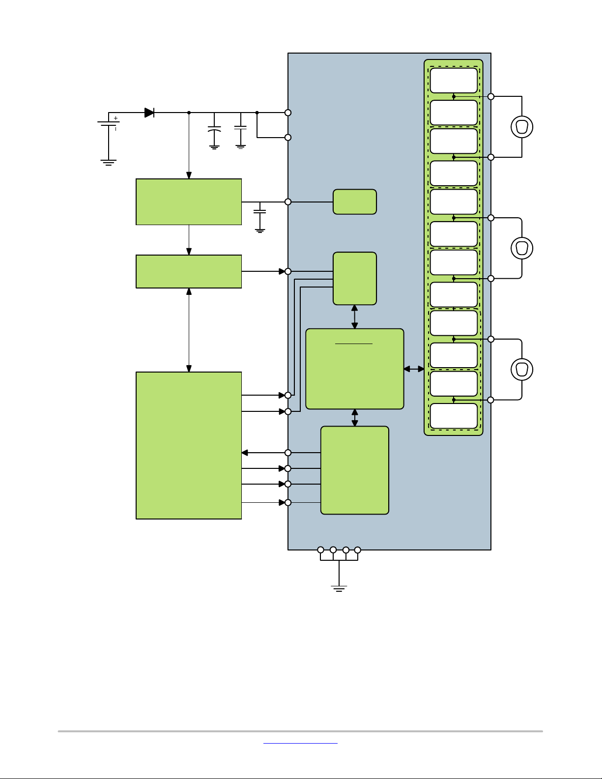
Typical Applications
• Automotive
• Industrial
• DC Motor Management for HVAC Application
© Semiconductor Components Industries, LLC, 2018
February, 2020 − Rev. 1
1 Publication Order Number:
NCV7723B/D
NCV7723B
13.2 V
10 mF 0.1 mF
Voltage
Regulator
Watchdog
VS1
VS2
VCC
0.1 mF
EN
PWM1
PWM2
NCV7723B
Power On
Reset
Control
Logic
Protection:
Under Load
Over Temperature
Under−voltage
Over−voltage
Over Current
High−side
Driver
Low−side
Driver
HS
LS
HS
LS
HS
LS
HS
LS
High−side
Driver
Low−side
Driver
OUT1
OUT2
OUT3
OUT4
OUT5
OUT6
uC
SO
SI
SCLK
CSB
16−Bit
Serial
Data
Interface
GND
Figure 1. Typical Application
www.onsemi.com
2
NCV7723B
VS1
EN
VCC
SO
SCLK
CSB
PWM1
PWM2
VS
ENABLE
POR
SI
VS1,
VS2
Overvoltage
BIAS
SPI and 16 Bit Logic Control
Lockout
Fault
Reporting
VS1
VS1
VS2
VS2
Charge
Pump
Control
Logic
Fault
DRIVE1
Wave Shaping
Wave Shaping
VS
HS+ LS Under Load
Overcurrent
Thermal Warning &
Shutdown
DRIVE 2
DRIVE 3
DRIVE 4
VS
High Side
Driver
OUT1
Low Side
Driver
OUT2
OUT3
OUT4
Undervoltage
Lockout
GND
GND
OUT1
OUT5
NC
VCC
SO
EN
NC
OUT6
OUT4
GND
SI
GND
GND
GND
Figure 2. Block Diagram
1
2
3
4
5
6
7
8
9
10
11
12 13
EPAD
VS2
24
23
22
21
20
19
18
17
16
15
14
VS1
VS2
GND
OUT2
NC
VS1
SCLK
CSB
PWM2
PWM1
VS2
NC
OUT3
GND
DRIVE 5
DRIVE 6
OUT5
OUT6
Figure 3. Pinout – SSOP24 NB EP
www.onsemi.com
3

NCV7723B
PIN FUNCTION DESCRIPTION The pin−out for the Half−Bridge Driver in SSOP24 NB EP package is shown in the table below.
Pin#
SSOP24
1 GND Ground. Must be connected to other GND pins externally.
2 OUT1 Half−bridge output 1
3 OUT5 Half−bridge output 5
4 NC No Connection. This pin should be isolated from any traces or via on the PCB board.
5 SI 16 bit serial communication input. 3.3 V / 5 V (TTL) Compatible − internally pulled down.
6 VCC Power supply input for Logic.
7 SO 16 bit serial communication output. 3.3 V / 5 V Compliant
8
9 NC No Connection. This pin should be isolated from any traces or via on the PCB board.
10 OUT6 Half−bridge output 6
11 OUT4 Half−bridge output 4
12 GND Ground. Must be connected to other GND pins externally.
13 GND Ground. Must be connected to other GND pins externally.
14 OUT3 Half−bridge output 3
15 NC No Connection. This pin should be isolated from any traces or via on the PCB board.
16 VS2 Power Supply input for outputs 3, 4, and 6. This pin must be connected to VS1 externally.
17 PWM1 External PWM input for output 1. 3.3 V / 5 V (TTL) Compatible − internally pulled down. Connect to ground or
18 PWM2 External PWM input for output 2. 3.3 V / 5 V (TTL) Compatible − internally pulled down. Connect to ground or
19
20 SCLK Serial communication clock input. 3.3 V / 5 V (TTL) Compatible − internally pulled down.
21 VS1 Power Supply input for outputs 1, 2, and 5. This pin must be connected to VS2 externally.
22 NC No Connection. This pin should be isolated from any traces or via on the PCB board.
23 OUT2 Half−bridge output 2
24 GND Ground. Must be connected to other GND pins externally.
EPAD Exposed Pad Connect to GND or leave unconnected.
Symbol Description
EN Enable − active high; wakes the device from sleep mode. 3.3 V / 5 V (TTL) Compatible − internally pulled down.
leave floating if unused.
leave floating if unused.
CSB Chip select bar − active low; enables serial communication operation. 3.3 V / 5 V (TTL) Compatible − internally
pulled up.
MAXIMUM RATINGS (Voltages are with respect to GND)
Rating
VSx Pin Voltage (VS1, VS2)
(DC)
(AC), t < 500 ms, Ivsx > −2 A
Pin Voltage (Vcc, SI, SCLK, CSB, SO, EN, PWM1, PWM2) VioMax −0.3 to 5.5 V
OUTx Pin Voltage
(DC)
(AC)
(AC), t < 500 ms, IOUTx > −1.1 A
(AC), t < 500 ms, IOUTx < 1 A
OUTx Pin Current (OUT1, ..., OUT6) IoutxImax −2.0 to 2.0 A
Junction Temperature Range T
Storage Temperature Range Tstr −55 to 150 °C
Peak Reflow Soldering Temperature: Pb−free 60 to 150 seconds at 217°C (Note 1) 260 °C
Stresses exceeding those listed in the Maximum Ratings table may damage the device. If any of these limits are exceeded, device functionality
should not be assumed, damage may occur and reliability may be affected.
1. See or download ON Semiconductor’s Soldering and Mounting Techniques Reference Manual, SOLDERRM/D.
Symbol Value Unit
VsxdcMax
VSxac
VoutxDc
VoutxAc
J
−0.3 to 45
−1.0
−0.3 to 45
−0.3 to 45
−1.0
1.0
−40 to 150 °C
V
V
www.onsemi.com
4
NCV7723B
ATTRIBUTES
Characteristic Symbol Value Unit
Short Circuit Reliability Characterization AECQ10x Grade A
ESD Capability
Human Body Model per AEC−Q100−002 VSx, OUTx
All Other Pins
Charged Device Model per AEC−Q100−011
Moisture Sensitivity Level MSL MSL2
Package Thermal Resistance – Still−air
Junction–to–Ambient (Note 2)
Junction–to–Board (Note 2)
2. Based on JESD51−7, 1.6 mm thick FR4, 2S2P PCB with 600 mm2 2 oz. copper and 18 thermal vias to 80x80 mm 1 oz. internal spreader
planes. Simulated with each channel dissipating 0.2 W.
RECOMMENDED OPERATING CONDITIONS
Parameter Symbol Min Max Unit
Digital Supply Input Voltage VCCOp 3.15 5.25 V
Battery Supply Input Voltage (VS1 = VS2) VSxOp 5.5 32 V
DC Output Current IxOp − 0.5 A
Junction Temperature TjOp −40 125 °C
Functional operation above the stresses listed in the Recommended Operating Ranges is not implied. Extended exposure to stresses beyond
the Recommended Operating Ranges limits may affect device reliability.
Vesd4k
Vesd2k
Vesd750
R
q
JA
R
Y
JBOARD
≥ ±4.0 kV
≥ ±2.0 kV
≥ ±750 V
32.1
21.8
°C/W
°C/W
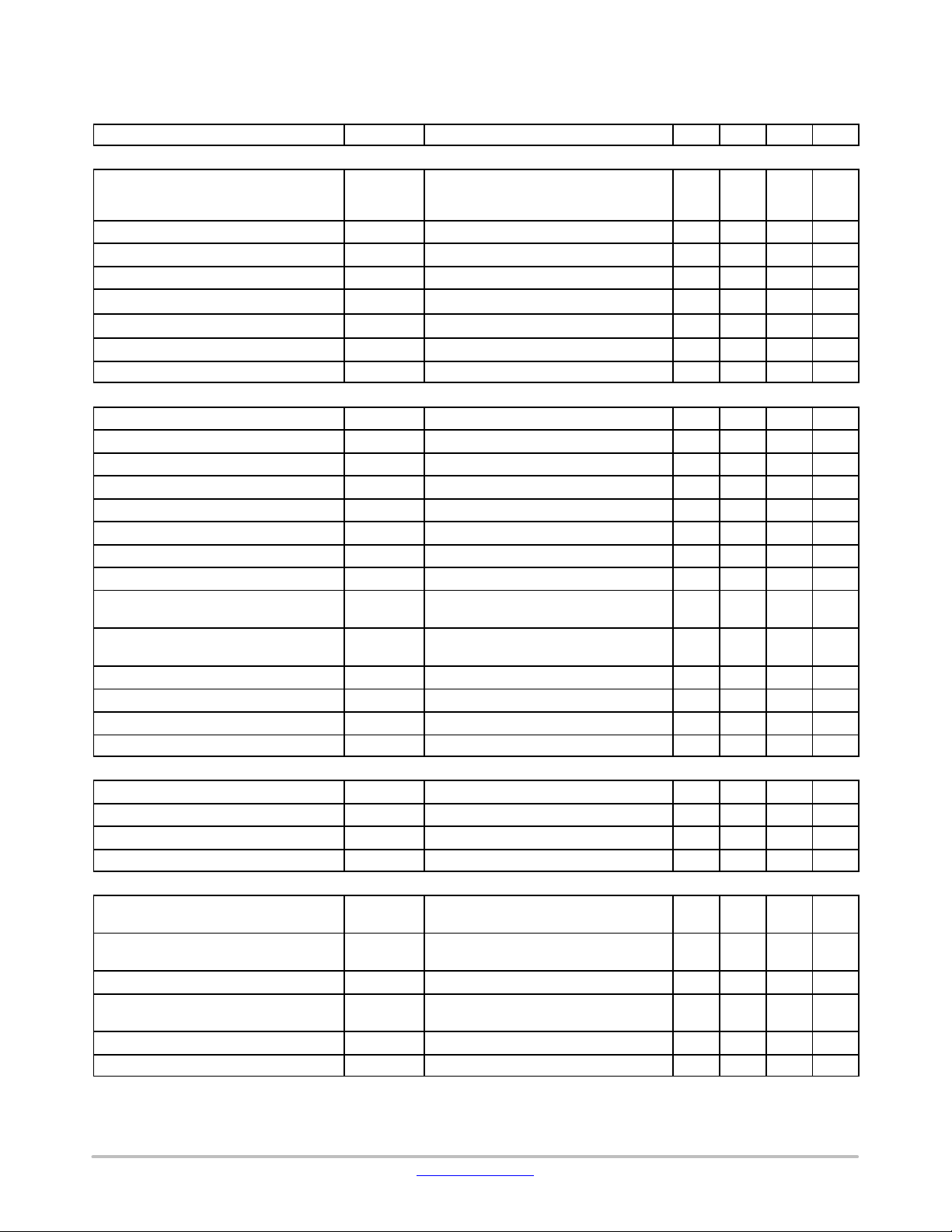
ELECTRICAL CHARACTERISTICS
(−40°C ≤ T
POWER SUPPLIES
Supply Current (VS1 + VS2)
Supply Current (VS1 + VS2)
Supply Current (Vcc)
Total Sleep Mode Current
VCC Power−on Reset Threshold VCCpor V
VSx Undervoltage Detection Threshold VSxuv VSx decreasing
VSx Undervoltage Detection Hysteresis VSxuHys 100 − 450 mV
VSx Overvoltage Detection Threshold VsXov VSx increasing
VSx Overvoltage Detection Hysteresis VSxoHys − 2.5 − V
DRIVER OUTPUT CHARACTERISTICS
Output High R
Output Low R
Source Leakage Current
≤ 150°C, 5.5 V ≤ VSx ≤ 40 V, 3.15 V ≤ VCC ≤ 5.25 V, EN = VCC, unless otherwise specified.)
J
Characteristic
Sleep Mode
Symbol Conditions Min Typ Max Unit
IqVSx85 VS1 = VS2 = 13.2 V, V
−40°C to 85°C
CC
= 0 V
IvsOp EN = VCC, 5.5V < VSx < 32 V
Active Mode
No Load,All Outputs Off
CSB = VCC, EN = SI = SCLK = 0 V
Sleep Mode
Active Mode
IqV
CC
IVCCOp
EN = CSB = V
−40°C to 85°C
, SI = SCLK = 0 V
CC
No Load, All Outputs Off
IqTot Sleep Mode, −40°C to 85°C
I(VS1) + I(VS2) + I(VCC)
VS1 = VS2 = 13.2 V, No Load
increasing − 2.70 2.90 V
CC
VSx increasing
VSx decreasing
(source) RDSonHS Iout = −500 mA, Vs = 13.2 V
DS(on)
(sink) RDSonLS Iout = 500 mA, Vs = 13.2 V
DS(on)
IsrcLkg13.2
IsrcLkg28
V
= 3.15 V
CC
V
= 3.15 V
CC
V
= 5 V, OUT (1−6) = 0 V, EN = 0/5 V
CC
VSx = 13.2 V
VSx = 28 V
− 1.0 2.5
−
0.5 1.0 mA
−
1.0
2.5
−
1.5
3.0
− 2.0 5.0
3.5
4.1
4.3
4.5
4.7
3.7
32
29.53633.54037.5
− 0.8 1.8
− 0.8 1.8
−1.0
−2.0−−
−
−
mA
mA
mA
mA
V
V
W
W
mA
mA
www.onsemi.com
5
NCV7723B
ELECTRICAL CHARACTERISTICS
(−40°C ≤ T
DRIVER OUTPUT CHARACTERISTICS
Sink Leakage Current
Overcurrent Shutdown Threshold (Source) IsdSrc V
Overcurrent Shutdown Threshold (Sink) IsdSnk V
Over Current Delay Timer TdOc 10 25 50
Underload Detection Threshold (Low Side) IuldLS
Underload Detection Threshold (High Side)
Underload Detection Delay Time TdUld V
Body Diode Forward Voltage IbdFwd If = 500 mA − 0.9 1.3 V
DRIVER OUTPUT SWITCHING CHARACTERISTICS
High Side Turn On Time
High Side Turn Off Time ThsOff
Low Side Turn On Time TlsOn
Low Side Turn Off Time TlsOff
High Side Rise Time ThsTr
High Side Fall Time ThsTf
Low Side Rise Time TlsTr
Low Side Fall Time TlsTf
High Side Off to Low Side On
Non−Overlap Time
Low Side Off to High Side On
Non−Overlap Time
PWM High to High Side On Time ThsOnPWM
PWM Low to High Side Off Time ThsOffPWM
PWM High to Low Side On Time TlsOnPWM
PWM Low to Low Side Off Time TlsOffPWM
THERMAL RESPONSE
Thermal Warning
Thermal Warning Hysteresis TwHy (Note 3) − 20 − °C
Thermal Shutdown Ts d (Note 3) 150 175 200 °C
Thermal Shutdown Hysteresis TsdHy (Note 3) − 20 − °C
LOGIC INPUTS − EN, SI, SCLK, CSB, PWM1, PWM2
Input Threshold High
Input Hysteresis − SI, SCLK, CSB, PWM1,
PWM2
Input Hysteresis − EN VthENHys 150 400 800 mV
Pull−down Resistance − EN, SI, SCLK,
PWM1, PWM2
Pull−up Resistance − CSB RpuCSB CSB = 0 V 50 125 250
Input Capacitance Cinx (Note 3) − − 15 pF
≤ 150°C, 5.5 V ≤ VSx ≤ 40 V, 3.15 V ≤ VCC ≤ 5.25 V, EN = VCC, unless otherwise specified.) (continued)
J
Characteristic UnitMaxTypMinConditionsSymbol
IsnkLkg13.2
IsnkLkg28
IuldHS
ThsOn
ThsOffLsOn
TlsOffHsOn
OUT (1−6) = VSx = 13.2 V
OUT (1−6) = VSx = 28 V
= 5 V, VSx = 13.2 V −2.0 −1.5 −1.1 A
CC
= 5 V, VSx = 13.2 V 1.1 1.5 2.0 A
CC
V
= 5 V, VSx = 13.2 V
CC
V
= 5 V, VSx = 13.2 V −7.5 −2.5 − mA
CC
= 5 V, VSx = 13.2 V 200 350 600
CC
Vs = 13.2 V, R
Vs = 13.2 V, R
Vs = 13.2 V, R
Vs = 13.2 V, R
Vs = 13.2 V, R
Vs = 13.2 V, R
Vs = 13.2 V, R
Vs = 13.2 V, R
Vs = 13.2 V, R
Vs = 13.2 V, R
Vs = 13.2 V, R
Vs = 13.2 V, R
Vs = 13.2 V, R
Vs = 13.2 V, R
load
load
load
load
load
load
load
load
load
load
load
load
load
load
= 70 W
= 70 W
= 70 W
= 70 W
= 70 W
= 70 W
= 70 W
= 70 W
= 70 W
= 70 W
= 70 W
= 70 W
= 70 W
= 70 W
−
−
− 2.5 7.5
− 120 165
− 20 45
− 120 165
− 35 75
10 30 50
10 30 50
10 30 50
10 30 50
5 − −
5 − −
− 120 165
− 20 45
− 120 165
− 35 75
V
= 5 V, EN = 0/5 V
CC
Twr (Note 3) 120 140 170 °C
Low
VthInH
VthInL
2.0
−
VthInHys 50 150 300 mV
Rpdx EN = SI = SCLK = V
CC
50 125 200
−
1.0
−
2.0
mA
mA
ms
mA
ms
ms
ms
ms
ms
ms
ms
ms
ms
ms
ms
ms
ms
ms
ms
−
−
0.6
−
V
V
kW
kW
www.onsemi.com
6

NCV7723B
ELECTRICAL CHARACTERISTICS
(−40°C ≤ T
LOGIC OUTPUT − SO
Output High
Output Low VsoL ISINK = 1.6 mA − − 0.4 V
Tri−state Leakage ItriStLkg CSB = 5 V −5 − 5
Tri−state Output Capacitance ItriStCout CSB = VCC, 0 V < V
SERIAL PERIPHERAL INTERFACE
SCLK Frequency
SCLK Clock Period TpClk V
SCLK High Time TclkH 1 85 − − ns
SCLK Low Time TclkL 2 85 − − ns
SCLK Setup Time TclkSup 3, 4 85 − − ns
SI Setup Time TsiSup 11
SI Hold Time TsiH 12
CSB Setup Time TcsbSup 5, 6
CSB High Time TcsbH (Note 4) 7
SO enable after CSB falling edge TenSo 8
SO disable after CSB rising edge TdisSo 9
SO Rise/Fall Time TsoR/F Cload = 40 pF (Note 3) − − 10 25 ns
SO Valid Time TsoV Cload = 40 pF (Note 3)
EN Low Valid Time TenL V
EN High to SPI Valid TenHspiV −
SRR Delay Between Consecutive Frames Tsrr (Note 5) −
Product parametric performance is indicated in the Electrical Characteristics for the listed test conditions, unless otherwise noted. Product
performance may not be indicated by the Electrical Characteristics if operated under different conditions.
3. Not production tested.
4. This is the minimum time the user must wait between SPI commands.
5. This is the minimum time the user must wait between consecutive SRR requests.
≤ 150°C, 5.5 V ≤ VSx ≤ 40 V, 3.15 V ≤ VCC ≤ 5.25 V, EN = VCC, unless otherwise specified.) (continued)
J
Characteristic UnitMaxTypMinConditionsSymbol
VsoH ISOURCE = −1 mA V
< 5.25 V (Note 3) − − 15 pF
CC
CC
0.6
–
Fclk − − − 5.0 MHz
= 5 V
CC
V
= 3.3 V −
CC
200
500
50
50
100
5.0
−
−
10
−
SCLK ↑ to SO 50%
= 5 V; EN H → L 50% to
CC
OUTx turning off 50%
−
10
−
150
− − V
mA
−
−
−
ns
−
− − ns
− − ns
− − ns
− −
ms
− 200 ns
− 200 ns
50 100 ns
− −
− 100
− −
ms
ms
ms
www.onsemi.com
7
NCV7723B
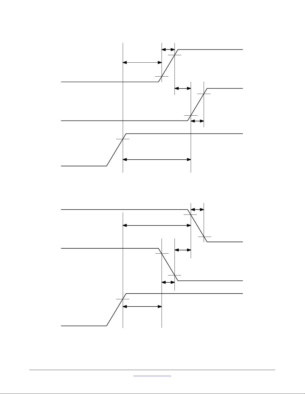
CHARACTERISTIC TIMING DIAGRAMS
TlsTr
TlsOff
90%
LS Turn OFF
HS Turn ON
CSB
LS Turn On
10%
TlsOffHsOn
90%
10%
ThsTr
90%
ThsOn
TlsTf
90%
TlsOn
HS Turn Off
CSB
10%
ThsOffLsOn
90%
10%
ThsTf
90%
ThsOff
Figure 4. Detailed Driver Timing
www.onsemi.com
8

NCV7723B
LS Turn On
HS Turn ON
PWMx
TlsTf
90%
TlsOnPWM
10%
90%
10%
ThsTr
90%
ThsOnPWM
LS Turn Off
HS Turn Off
PWMx
90%
TlsOffPWM
10%
90%
ThsOffPWM
TlsTr
90%
10%
ThsTf
Figure 5. Detailed Driver Timing (OUT1 / OUT2 PWM)
www.onsemi.com
9
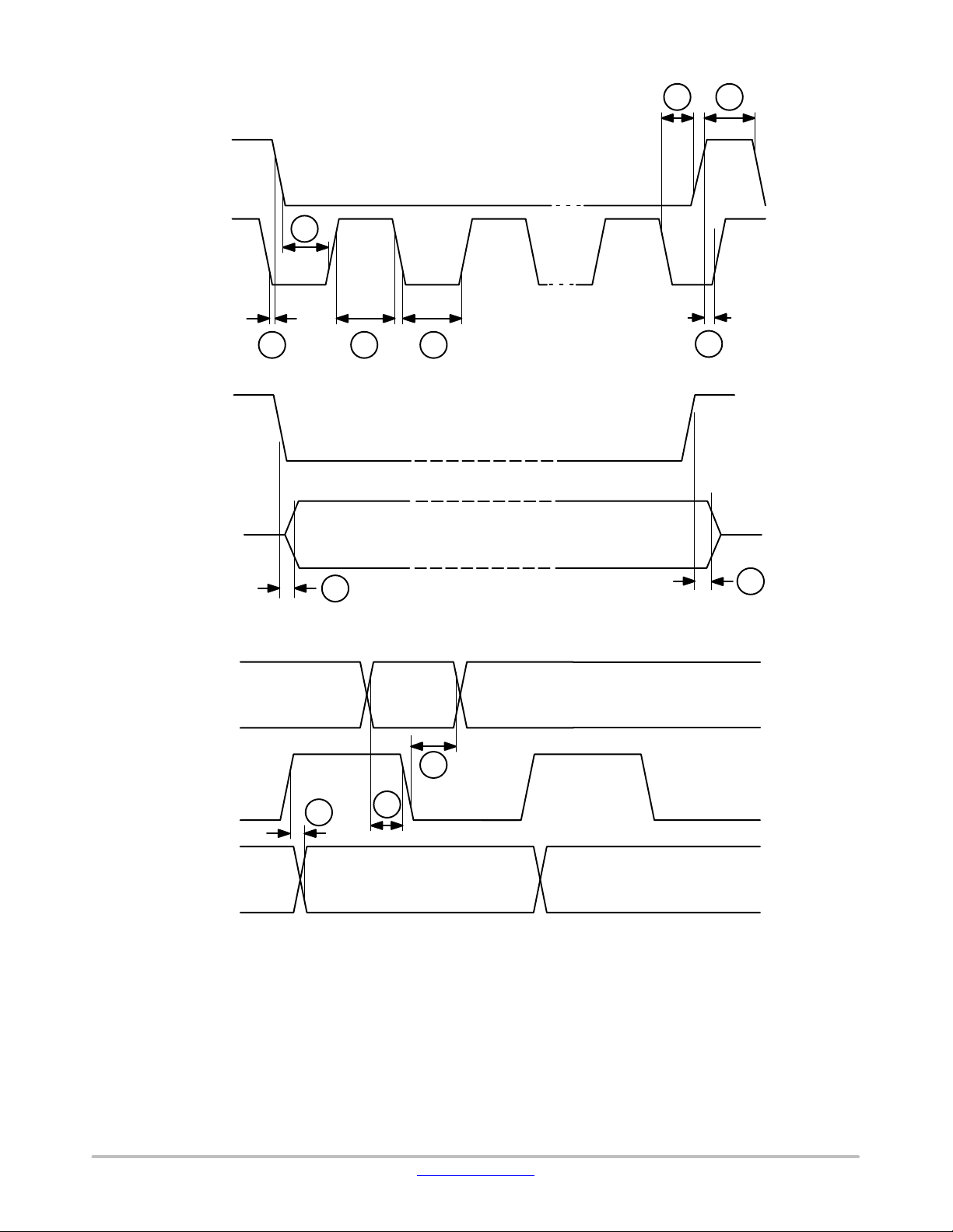
CSB
SCLK
NCV7723B
4 7
5
CSB
SO
SI
SCLK
3 1 2
8
12
10
11
6
9
SO
Figure 6. Detailed SPI Timing
www.onsemi.com
10

NCV7723B
TYPICAL PERFORMANCE GRAPHS
3.5
3.0
2.5
2.0
1.5
1.0
0.5
IqTot, TOTAL SLEEP MODE CURRENT (mA)
1.8
1.6
1.4
(W)
1.2
DS(on)
R
1.0
0.8
0
VSx = 13.2 V
1.40
VSx = 13.2 V
VSx = 13.2 V
VCC = 5.25 V
VCC = 5 V
1.38
1.36
1.34
1.32
CURRENT (mA)
1.30
CC
1.28
150°C
25°C
1.26
VCC = 3.15 V
0 100
15050−50
1.24
1.22
ACTIVE MODE V
1.20
−40°C
TEMPERATURE (°C) VCC VOLTAGE (V)
Figure 7. IqTot vs. Temperature Figure 8. I(VCC) Active Mode vs. V(VCC)
1.0
If = 0.5 A
0.95
0.9
HSx
LSx
0.85
LSx
0.8
HSx
5.55.04.54.03.53.0
0.6
TEMPERATURE (°C)
Figure 9. R
DS(on)
1.7
1.6
1.5
1.4
VSx = 13.2 V
= 5.0 V
V
1.3
CC
IsdSrc, IsdSnk OVERCURRENT (A)
1.2
TEMPERATURE (°C)
Figure 11. Overcurrent vs. Temperature Figure 12. Leakage vs. Temperature
0.75
BODY DIODE FORWARD VOLTAGE (V)
150100500−50
TEMPERATURE (°C)
vs. Temperature Figure 10. Body Diode vs. Temperature
0.2
VSx = 13.2 V
LSx
HSx
0.18
0.16
0.14
(mA)
0.12
0.1
snkLkg
, I
0.08
0.06
srcLkg
I
0.04
0.02
150100500−50
0
= 5 V
V
CC
I
snk
I
src
TEMPERATURE (°C)
150100500−50
150100500−50
www.onsemi.com
11

NCV7723B
DETAILED OPERATING DESCRIPTION
General Overview
The NCV7723B is comprised of twelve NMOS power
drivers. The drivers are arranged as six half−bridge output
channels, allowing for three independent full−bridge
configured loads. Output control and status reporting is
handled via the SPI (Serial Peripheral Interface)
communications port. OUT1 and OUT2 can be controlled
with an external PWM signal.
Each output is characterized for a typical 0.5 A DC load
and has a maximum 2.0 A surge capability (at VSx =
13.2 V). Maximum allowable junction temperature is
150°C and may constrain the maximum load current and/or
limit the number of drivers active at once.
An active−high enable function (EN) allows global
control of the outputs and provides a low quiescent current
sleep mode when the device is not being utilized. An internal
pull−down resistor is provided on the input to ensure the
device enters sleep mode if the input signal is lost.
After EN transitions from low to high, the V
POR cycle
CC
will proceed and bring the device into normal operation. The
device configuration registers can then be programmed via
SPI. Bringing EN low clears all registers (no configuration
or status data is stored), disables the drivers, and enters sleep
mode.
SPI Communication
16−bit full duplex SPI communication has been
implemented for device configuration, driver control, and
reading the status data. In addition to the 16−bit status data,
a pseudo−bit (PRE_15) can also be retrieved from the SO
output.
The device must be enabled (EN = H) for SPI
communication. The SPI inputs are TTL compatible and the
SO output high level is defined by the applied V
CC
. The
active−low CSB input has a pull−up resistor and the
remaining inputs have pull−down resistors to bias them to
known states when SPI communication is inactive.
The latched thermal shutdown (TSD) status bit PRE_15
is available on SO until the first rising SCLK edge after CSB
goes low. The following conditions must be met for a valid
TSD read to be captured:
1. SCLK and SI are low before the CSB cycle;
2. CSB transitions from high to low;
3. CSB setup time (TcsbSup: Figure 6, #5) is
satisfied.
Figure 13 shows the SPI communication frame format,
and Tables 1 and 2 define the command input and diagnostic
status output bits.
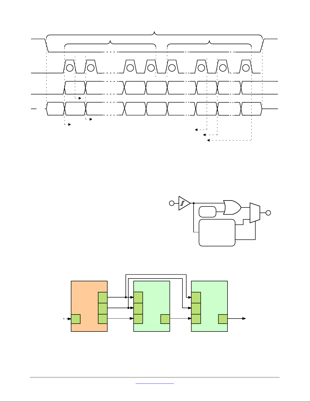
CSB
SI
SCLK
SO
PRE_15
PSEUDO−BIT
SRR HBSEL ULDSC
15 14 13 0
OCS PSF ULDTSD TW
Figure 13. SPI Communication Frame Format
Communication is implemented as follows and is also
illustrated in Figures 13 and 15:
1. SI and SCLK are set low before the CSB cycle.
2. CSB goes low to begin a serial data frame;
pseudo−bit PRE_15 is immediately available at
SO.
3. SI data is shifted in on every rising edge of SCLK,
starting with the most significant bit (MSB), SRR.
4. SI data is recognized on every falling edge of the
SCLK.
B[12:7] → HBEN[6:1]
B[12:7] → HBST[6:4]
Communication is implemented as follows and is also
illustrated in Figures 13 and 15:
1. SI and SCLK are set low before the CSB cycle.
2. CSB goes low to begin a serial data frame;
pseudo−bit PRE_15 is immediately available at
SO.
3. SI data is shifted in on every rising edge of SCLK,
starting with the most significant bit (MSB), SRR.
4. SI data is recognized on every falling edge of the
SCLK.
B[6:1] → HBCNF[6:1]
B[6:1] → HBST[3:1]
OVLO
www.onsemi.com
12

NCV7723B
Table 1. SPI COMMAND INPUT DEFINITIONS
Channels 6 – 1
Bit# Name Function Status* Scope
15 SRR Status Register Reset** 1 = Reset Global Status Reset
14 HBSEL*** Half Bridge Selection Reserved −
13 ULDSC Underload Shutdown Control 1 = Enabled Per Half−Bridge Operation
12 HBEN6 Enable Half−Bridge 6
11 HBEN5 Enable Half−Bridge 5
10 HBEN4 Enable Half−Bridge 4
9 HBEN3 Enable Half−Bridge 3
8 HBEN2 Enable Half−Bridge 2
7 HBEN1 Enable Half−Bridge 1
6 HBCNF6 Configure Half−Bridge 6
5 HBCNF5 Configure Half−Bridge 5
4 HBCNF4 Configure Half−Bridge 4
3 HBCNF3 Configure Half−Bridge 3
2 HBCNF2 Configure Half−Bridge 2
1 HBCNF1 Configure Half−Bridge 1
0 OVLO VSx Overvoltage Lockout 1 = Enabled Global Lockout
*All command input bits are set to 0 at V
**Latched faults are cleared and outputs can be re−programmed if no fault exists after SRR asserted.
***HBSEL enables channel group selection for family devices with more than 6 channels. In the NCV7723B it is recommended to set the HBSEL
bit to 0.
power−on reset.
CC
0 = Hi−Z
1 = Enabled
0 = LS On, HS Off
1 = LS Off, HS On
Per Half−Bridge
Per Half−Bridge
www.onsemi.com
13
NCV7723B
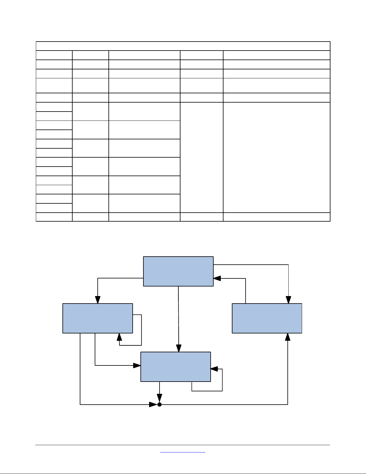
Table 2. SPI STATUS OUTPUT DEFINITIONS
Channels 6 – 1
Bit# Name Function Status* Scope
PRE_15 TSD Latched Thermal Shutdown 1 = Fault Global Notification; Per Half−Bridge Operation
15 OCS Latched Overcurrent Shutdown 1 = Fault Global Notification; Per Half−Bridge Operation
14 PSF
13 ULD Underload Detect 1 = Fault Global Notification; Per Half−Bridge Operation
12
11
10
9
8
7
6
5
4
3
2
1
0 TW Thermal Warning 1 = Fault Global Notification; Per Half−Bridge Operation
*All status output bits are set to 0 at Vcc power−on reset (POR).
HBSTx[1:0] bits are priority encoded to provide the status information of each of the half−bridge outputs. Figure 14 shows the priority encoding
state diagram for the HBSTx[1:0] bits.
HBST6[1:0] Half Bridge 6 Output Status
HBST5[1:0] Half Bridge 5 Output Status
HBST4[1:0] Half Bridge 4 Output Status
HBST3[1:0] Half Bridge 3 Output Status
HBST2[1:0] Half Bridge 2 Output Status
HBST1[1:0] Half Bridge 1 Output Status
VS1 and/or VS2
Undervoltage or Overvoltage
1 = Fault Global Notification; Global Operation
0x00b – Output
Disabled
0x01b − OCS
0x10b − ULD
0x11b − Output
Enabled
Per Half−Bridge
PSF, TSD
HBENx = ‘0’
Power On Reset
Under
Load
ULD
“10”
Over
Current
*PSF Recovery: VSx rising above the undervoltage threshold or falling below the overvoltage threshold (OVLO = 1)
**TSD Recovery: Sending SRR after junction temperature has fallen below the thermal shutdown threshold
PSF
TSD
Output Enabled
“11”
Over
Current
OCS
“01”
HBENx = ‘1’
PWMx = ‘1’
PSF Recovery*
TSD Recovery**
Output Disabled
“00”
(default)
PSF
TSD
SRR = ‘1’
Power On Reset
Figure 14. SO HBSTx [1:0] Priority Encoding State Diagram
www.onsemi.com
14

NCV7723B
Priority Encoding
If an under load event precedes an over current event on
the same half−bridge, the device will report HBSTx = ‘10’
and then HBSTx = ‘01’ as shown in Figure 14. An over
current event preceding an under load event will report
HBSTx = ‘01’ since there is no direct path from the OCS
state to the ULD state. Thus an over current shutdown fault
must be cleared before an underload fault is reported on the
same half−bridge.
Frame Error Detection
The NCV7723B employs frame error detection to help
ensure input data integrity. SCLK is compared to an n x 8 bit
counter and a valid frame (CSB H−L−H cycle) has integer
multiples of 8 SCLK cycles. For the first 16 bits shifted into
SI, SCLK is compared to a modulo16 counter (n = 2), and
SCLK is compared to a modulo 8 counter (n = 1, 2, ...m)
thereafter. This variable modulus allows for daisy chain
operation with devices using different word lengths.
The last 16 bits clocked into SI are transferred to the
NCV7723B’s data register if no frame error is detected,
otherwise the entire frame is ignored and the previous input
data is preserved.
Daisy Chain Operation
Daisy chain operation is possible with multiple 16−bit and
8−bit devices that have a compatible SPI protocol. The clock
phase and clock polarity with respect to the data for all the
devices in the chain must be the same as the NCV7723B.
CSB and SCLK are parallel connected to every device in
the chain while SO and SI are series connected between each
device. The master’s MOSI is connected to the SI of the first
device and the first device’s SO is connected to the next
device’s SI. The SO of the final device in the chain is
connected to the master’s MISO.
The hardware configuration for the NCV7723B daisy
chained with an 8−bit SPI device is shown in Figure 15.
A24−bit frame made of 16−bit word ‘A’ and 8−bit word ‘B’
is sent from the master. Command word B is sent first
followed by word A. The master simultaneously receives
status word B first followed by word A. The progression of
data from the MCU through the sequential devices is
illustrated in Figure 15.
Compliance with the illustrated frame format is required
for proper daisy chain operation. Situations should be
avoided where an incorrect multiple of 8 bits is sent to the
devices, but the frame length does not cause a frame error in
the devices. For example, the word order could be
inadvertently interleaved or reversed. Invalid data is
accepted by the NCV7723B in such scenarios and possibly
by other devices in the chain, depending on their frame error
implementation. Data is received as a command by the
device at the beginning of the chain, but the device at the end
of the chain may receive status data from the preceding
device as a command.
MISO
MCU
Master
CSB
SCLK
MOSI
CMD [x, n] = Command Word to Device ‘x’, Length ‘n’
STA [x, n] = Status Word from Device ‘x’, Length ‘n’
NCV7723B
16−bit Device
CSB
SCLK
SO
STA [A, 16]
CMD [B, 8]
CMD [B, 8]
+
CMD [A, 16]
Figure 15. Daisy Chain Configuration
SI
Device A
8−bit Device
CSB
SCLK
SI
+
Device B
SO
STA [B, 8]
+
STA [A, 16]
www.onsemi.com
15
CSB
NCV7723B
24 bit Frame
Word B − 8 bits Word A − 16 bits
SCLK
SI
TSDSO MSB
7 6 1 0 15
MSB
SI data is recognized on the falling SCLK. edge
SO data is shifted out on the rising SCLK edge.
Modulo 16 counter begins on the first rising SCLK edge after CSB goes low.
Modulo 16 counter ends − 16 bit word length valid.
Modulo 8 counter begins on the next rising SCLK edge.
Modulo 8 counter ends − 8 bit word length valid. valid n*8 bit frame.
Figure 16. Daisy Chain – 24 bit Frame Format
TSD Bit in Daisy Chain Operation
The SO frame is designed to allow TSD status retrieval in
a daisy chain configuration using NCV7723B or other
devices with identical SPI functionality. The TSD status bit
is OR’d with SI and then multiplexed with the device’s usual
status data (Figure 17).
CSB is held high and SI and SCLK are held low by the
master before the start of the SPI frame. TSD status is
immediately available as bit PRE_15 at SO (SO = TSD)
when CSB goes low to begin the frame. The usual status data
(SO = STA) becomes available after the first rising SCLK
edge.
The TSD status automatically propagates through the
chain from the SO output of the previous device to the SI
input of the next. This is shown in Figures 18 and 19, first
without a TSD fault in either device (Figure 18), and then
subsequently with a latched TSD fault (TSD = 1) in device
“A” propagating through to device “B” (Figure 19).
0
LSB
LSB
LSB
LSB
8 7
MSB
MSB
Since the TSD status of any device propagates
automatically through the entire chain, it is not possible to
determine which device (or devices) has a fault (TSD = 1).
The usual status data from each device will need to be
examined to determine where a fault (or faults) may exist.
SI
TSD
SO
SI
SPI
SEL
Figure 17. TSD SPI Link
M
U
X
SO
MISO
MCU
Master
NCV7723B
CSB
SCLK
MOSI
1 → 0
0
0
CSB
SCLK
SI
Device A
No TSD No TSD
SO
Figure 18. Daisy Chain Without TSD Fault
www.onsemi.com
16
Z → 0
CSB
SCLK
SI
NCV7726B
or NCV7723B
Device B
SO
Z → 0

NCV7723B
NCV7723B
CSB
SCLK
SI
Latched TSD No TSD
MISO
MCU
Master
CSB
SCLK
MOSI
1 → 0
0
0
Figure 19. Daisy Chain With TSD Fault
Power Up/Down Control
The V
V
CC
power−up/down. V
supply input powers the device’s logic core. A
CC
power−on reset (POR) function provides controlled
POR initializes the command input
CC
and status output registers to their default states (0x00), and
ensures that the bridge output and SO drivers maintain Hi−Z
as power is applied. SPI communication and normal device
operation can proceed once V
rises above the POR
CC
threshold and EN remains high.
The VS1 and VS2 supply inputs power their respective
output drivers (refer to Figure 2 and the PIN FUNCTION
DESCRIPTION). The VSx inputs are monitored to ensure
that the supply stays within the recommended operating
range. If the VSx supply moves into either of the VS
undervoltage or overvoltage regions, the output drivers are
switched to Hi−Z but command and status data is preserved.
Output drivers will remain on if OVLO = 0 during an
overvoltage condition.
Driver Control
The NCV7723B has the flexibility to control each
half−bridge driver channel via SPI. Actual driver output
state is determined by the command input and the current
fault status bits.
High−side (HSx) and low−side (LSx) drivers of the same
channel cannot be active at the same time, and non−overlap
delays are imposed when switching between HSx and LSx
drivers in the same channel, preventing current
shoot−through.
After the device has powered up and the drivers are
allowed to turn on, the drivers remain on until commanded
off via SPI or until a fault condition occurs.
PWM Control
Outputs 1 and 2 can be controlled in two ways: through
normal SPI control (see Table 1) or from an external PWM
signal. OUT1 can be turned on/off using the HBEN1 bit or
NCV7726B
or NCV7723B
CSB
SCLK
Device A
SO
Z → 1
SI
Device B
SO
Z → 1
applying a logic level signal to pin 17 (PWM1). OUT2 can
be turned on/off using the HBEN2 bit or applying a logic
level signal to pin 18 (PWM2). Simplified logic functions
are shown below in Figure 20.
PWM Example: Turn on OUT1 High Side
To use OUT1 High Side with external PWM control,
perform the following steps:
1. Send command 0b0000000000000010 (0x0002)
♦ Configures OUT1 to High Side (HBCNF1)
♦ Disables OUT1 SPI Enable (HBEN1)
2. Apply logic level PWM signal to PWM1
To use OUT1 Low Side with external PWM, set the
HBCNF1 bit to 0 during step 1.
HBCNFx
HSx
HBENx
PWMx
LSx
PWMx HBENx HBCNFx HSx LSx OUTx
0 0 x OFF OFF Z
x 1 0 OFF ON Low
x 1 1 ON OFF High
1 x 0 OFF ON Low
1 x 1 ON OFF High
Figure 20. PWM Control Logic
VS
OUTx
GND
www.onsemi.com
17
NCV7723B
DIAGNOSTICS, PROTECTIONS, STATUS REPORTING AND RESET
Overview
The NCV7723B employs diagnostics designed to prevent
destructive overstress during a fault condition. Diagnostics
resolved. Table 4 shows output states during faults and
output recovery modes, and Table 5 shows the status
memory and memory clear modes.
are classified as either supervisory or protection functions
(Table 3). Supervisory functions provide status information
about device conditions. Protection functions provide status
Table 3. DIAGNOSTIC CLASSES AND FUNCTIONS
information and activate fault management behaviors.
Diagnostics resulting in output shutdown and latched status
may depend on a qualifier and may require user intervention
for output recovery and status memory clear. Diagnostics
resulting in output lockout and non−latched status (VSOV
or VSUV) may recover and clear automatically. Output
configurations can be changed during output lockout.
Outputs assume the new configurations or resume the
HBSTx[1:0] Supervisory Half−Bridge X Output Status
previous configurations when an auto−recover fault is
Table 4. OUTPUT STATE VS. FAULT AND OUTPUT RECOVERY
Fault Qualifier OUTx State OUTx Recovery OUTx Recovery Scope
TSD − → Z Send SRR All Outputs
OCS − → Z Send SRR All Outputs
PSF – VSOV
PSF – VSUV − → Z → Y
ULD
TW − Unaffected − −
*OUTx returns to its previous state (Yn) or new state (Yn+1) if fault is removed.
OVLO = 1 → Z → Y
OVLO = 0 Unaffected − −
ULDSC = 1 → Z Send SRR All Outputs
ULDSC = 0 Unaffected − −
| Y
n
n+1
| Y
n
n+1
Name Class Function
TSD Protection Thermal Shutdown
OCS Protection Overcurrent Shutdown
PSF Protection Under/overvoltage Lockout
(OVLO = 1)
ULD Protection Underload Shutdown
TW Supervisory Thermal Warning
Auto* All Outputs
Auto* All Outputs
Table 5. STATUS MEMORY VS. FAULT AND MEMORY CLEAR
Fault Qualifier Status Memory Memory Clear Memory Clear Scope
TSD − Latched Send SRR Global
OCS − Latched Send SRR Global
PSF – VSOV OVLO = X Non−Latched Auto* Global
PSF – VSUV
ULD ULDSC = X Latched Send SRR Global
TW − Non−Latched Auto* Global
*Status memory returns to its no−fault state if fault is removed.
−
Status Information Retrieval
Current status information is retrieved during each SPI
frame. To preserve device configuration and output states,
the previous SI data pattern must be sent during the status
retrieval frame.
Status information is prevented from being updated
during a SPI frame but new status becomes available after
CSB goes high at the end of the frame provided the frame did
not contain an SRR request. Status information includes
both global and per channel fault notification. To determine
the channel(s) affected after detecting a global fault,
examine driver output status and input configuration.
Non−Latched Auto* Global
Status Register Reset − SRR
Sending SRR = 1 clears status memory and re−activates
faulted outputs for all channels. The previous SI data pattern
must be sent with SRR to preserve device configuration and
output states.
At the rising edge of CSB, the SRR function is activated
and an internal timer (Tsrr) is started. Tsrr is the minimum
time the user must wait between consecutive SRR requests.
If a fault is still present when SRR is sent, protection will be
re−engaged and shutdown will recur. The status registers can
also be reset by toggling the EN pin or by VCC power−on
reset.
www.onsemi.com
18

NCV7723B
Diagnostics Details
The following sections describe individual diagnostics
and behaviors. In each description and illustration, a SPI
frame is assumed to always be valid and the SI data pattern
sent for HBCNFx and HBENx is the same as the previous
frame. Actual results can depend on asynchronous fault
events and SPI clock frequency and frame rate.
Undervoltage Lockout
Global Notification, Global Operation
Undervoltage detection and lockout control is provided
by monitoring the VS1, VS2 and VCC supply inputs.
Undervoltage hysteresis is provided to ensure clean
SO
Status
Output
State
SI
OUTx
LS
X
?
?
OUTx
LS
No
Fault
No Fault
OUTx GND
OUTx
LS
PSF
PSF
ALL
Z
detection transitions. Undervoltage timing is shown in
Figure 21.
Undervoltage at either VSx input turns off all outputs and
sets the power supply fail (PSF) status bit. The outputs return
to their previously programmed state and the PSF status bit
is cleared when VSx rises above the hysteresis voltage level.
SPI communication is available and programmed output
enable and configuration states are maintained if proper
VCC is present during VSx undervoltage. Output enable and
configuration states can also be programmed during VSx
undervoltage if proper VCC is present, and state changes
will take effect as VSx rises above the undervoltage
threshold level.
OUTx
LS
No
Fault
No
Fault
OUTx GND
OUTx
HS
Z
?
ALL
Z
OUTx
HS
0x00
0x00
OUTx
HS
No
Fault
No
Fault
OUTx VS
VSx
VSUV
Vcc
Figure 21. Undervoltage Timing
Overvoltage Lockout
Global Notification, Global Operation
Overvoltage detection and lockout control is provided by
monitoring the VS1 and VS2 supply inputs. Hysteresis is
provided to ensure clean detection transitions. Overvoltage
timing is shown in Figure 22. Overvoltage at either VSx
input turns off all outputs if the overvoltage lockout input bit
is set (OVLO = 1) and sets the power supply fail (PSF) status
bit (see Tables 4 and 5). The outputs return to their
previously programmed state and the PSF status bit is
cleared when VSx falls below the hysteresis voltage level.
VccUV
t
Output enable and configuration states can also be
programmed during an overvoltage lockout event but will
not change state until VSx falls below the overvoltage
threshold level.
NOTE: to reduce stress, it is recommended to operate the
device with OVLO bit asserted to ensure that the
drivers turn off during a load dump scenario. If
OVLO = 0 during an overvoltage condition,
outputs will remain on and the PSF status bit will
be set.
www.onsemi.com
19

NCV7723B
SO
Status
Output
State
VSx
SI
OUTx ON
OVLO = 0
X
?
?
OUTx
ON
No
Fault
No
Fault
OUTx
ON
PSF
PSF
OUTx
ON
VSOV
Figure 22. Overvoltage Timing
Overcurrent Shutdown
Global and per Channel Notification
Per Half−Bridge Operation
Overcurrent detection and shutdown control is provided
by monitoring each HS and LS driver. Overcurrent timing is
shown in Figure 23. Overcurrent in either driver starts a
channel’s overcurrent delay timer (TdOc). If overcurrent
exists after the delay, both drivers are latched off and the
OUTx ON
OVLO = 1
No
Fault
No
Fault
OUTx
ON
PSF
PSF
ALL
VSOV
OUTx
OFF
No
Fault
No
Fault
OUTx
Z
ON
No
Fault
OUTx Z
t
global overcurrent (OCS) status bit is set. The channel’s
corresponding HBSTx[1:0] bits are also set to “01” to
indicate an OCS fault. Note that OCS fault reporting has
priority over other faults as shown in Figure 14. The global
OCS bit and individual channel bits are cleared and channels
are re−activated by sending SRR = 1.
A persistent overcurrent cause should be resolved prior to
re−activation to avoid repetitive stress on the drivers.
SI
SO
Status
Output
State
Output
Current
OUTx ON
SRR = 0
No
Fault
No
Fault
OUTx
ON
OUTx
ON
No
Fault
TdOc
OUTx
ON
OCS
OCS
OUTx Z
IsdSxx
Figure 23. Overcurrent Timing
OUTx ON
SRR = 1
OCS
OUTx
ON
No
Fault
No
Fault
OUTx
ON
OUTx
ON
OCS
OCS
OUTx Z
TdOc
t
www.onsemi.com
20

NCV7723B
Underload Shutdown
Global and per Channel Notification
Global Shutdown Control, Per Half−Bridge Operation
Underload detection and shutdown control is provided by
monitoring each half bridge driver. Underload timing is
shown in Figure 24. Underload at any driver starts the global
underload delay timer. If underload occurs in another
channel after the global timer has been started, the delay for
any subsequent underload will be the remainder of the timer.
If underload exists after the global delay timer and if the
underload shutdown (ULDSC) command bit is set, both
HSand LS drivers are latched off and the global underload
SO
Status
Output
State
Output
Current
SI
LSx ON
ULDSC = 0
No
Fault
No Fault
OUTx
ON
LSx
ON
No
Fault
TdUld TdUld
LSx ON
SRR = 1
ULD
ULD
OUTx GND
(ULD) status bit is set along with the corresponding per
channel status bits HBSTx[1:0] set to “10”. Drivers will
remain on if the ULDSC input bit is 0 (see Table 4 and 5).
The global ULD bit and per channel HBSTx bits are cleared
and channels are re−activated by sending SRR = 1.
NOTE: underload may result from a fault (e.g. open−load)
condition or normal circuit behavior (e.g. L/R
tau). In motor applications it is often desirable to
actively brake the motor by turning on both HS or
LS drivers in two half−bridge channels which may
result in an underload condition as current decays.
LSx
ON
No
Fault
No Fault
OUTx GND
No
Fault
IuldLS
LSx ON
ULDSC = 1
ULD
LSx ON
SRR = 1
ULD
ULD
OUTx
Z
TdUld
Figure 24. Underload Timing
t
www.onsemi.com
21

Thermal Warning and Thermal Shutdown
NCV7723B
Global Notification, Per Half−Bridge Operation
Thermal warning (TW) and thermal shutdown (TSD)
detection and control are provided for each half−bridge by
monitoring the driver pair’s thermal sensor. Thermal
hysteresis is provided for each of the warning and shutdown
functions to ensure clean detection transitions. Software
polling of the TW bit allows for avoidance of thermal
shutdown since TW notification precedes TSD notification.
Thermal warning and shutdown timing is shown in
Figure 25.
SI
SO
Status
Output
State
T
TSD
OUTx
ON
No
Fault
No
Fault
J
OUTx
ON
TW
TW
OUTx ON
OUTx
ON
No
Fault
No
Fault
The TW status bit is set when a half−bridge’s sensor
temperature exceeds the warning level (T
> Twr), and the
J
bit is automatically cleared when sensor temperature falls
below the warning hysteresis level (T
< TwHy). A channel’s
J
output state is unaffected by TW.
When sensor temperature exceeds the shutdown level
(T
> Tsd), the channel’s HS and LS drivers are latched off,
J
the TW bit is/remains set, and the TSD (PRE_15) bit is set.
The TSD bit is cleared and all affected channels are
re−activated (T
OUTx
ON
TW
TW
< TsdHy) by sending SRR = 1.
J
OUTx ON
SRR = 1
TSD
TW
TSD
TW
TsdHy
OUTx ON
SRR = 1
TW
TW
OUTx Z
TW
OUTx
ON
TWR
TwHy
Figure 25. Thermal Warning and Shutdown Timing
The latched thermal shutdown (TSD) information is
available on SO after CSB transitions from high to low and
before the first rising SCLK edge. The following procedures
must be met for a true TSD reading:
1. SCLK and SI are low before the CSB cycle.
Violating these conditions will results in an
t
undetermined SPI behavior or/and an incorrect
TSD reading.
2. CSB transitioning from high to low.
3. CSB setup time (TcsbSup) is satisfied and the data
is captured before the first SCLK rising edge.
www.onsemi.com
22

NCV7723B
†
THERMAL PERFORMANCE ESTIMATES
Figure 26. Transient R(t) vs. Pulse Time for 2 oz Spreader
ORDERING INFORMATION
Device Package Shipping
NCV7723DQBR2G SSOP24 NB EP
(Pb−Free)
†For information on tape and reel specifications, including part orientation and tape sizes, please refer to our Tape and Reel Packaging
Specifications Brochure, BRD8011/D.
2500 / Tape & Reel
www.onsemi.com
23

MECHANICAL CASE OUTLINE
PACKAGE DIMENSIONS
SCALE 1:1
2X
NOTE 4
D
A
B
TOP VIEW
SIDE VIEW
NOTE 8
D2
BOTTOM VIEW
5.63
13
24X
A1
EE1
b
M
0.12 DC
E2
NOTE 8
2X
24X
0.20 C
NOTE 5
PIN 1
REFERENCE
0.10 C
0.10
M
0.15 DC
NOTE 6
24
112
e
NOTE 6
A
C
A-B
RECOMMENDED
SOLDERING FOOTPRINT
SSOP24 NB EP
CASE 940AK
C
A-B0.20
D
H
A1
0.20 C
2X 12 TIPS
A-B
A2
SEATING
C
PLANE
M
0.15 DC
ISSUE O
L
DETAIL A
NOTE 7
h
c
END VIEW
A-B
L1
DATE 24 APR 2012
NOTES:
1. DIMENSIONING AND TOLERANCING PER ASME
Y14.5M, 1994.
2. CONTROLLING DIMENSION: MILLIMETERS.
3. DIMENSION b DOES NOT INCLUDE DAMBAR
PROTRUSION. DAMBAR PROTRUSION SHALL
BE 0.10 MAX. AT MMC. DAMBAR CANNOT BE
L2
GAUGE
PLANE
SEATING
C
PLANE
DETAIL A
h
LOCATED ON THE LOWER RADIUS OF THE
FOOT. DIMENSION b APPLIES TO THE FLAT
SECTION OF THE LEAD BETWEEN 0.10 TO 0.25
FROM THE LEAD TIP.
4. DIMENSION D DOES NOT INCLUDE MOLD
FLASH, PROTRUSIONS OR GATE BURRS. MOLD
FLASH, PROTRUSIONS OR GATE BURRS SHALL
NOT EXCEED 0.15 PER SIDE. DIMENSION D IS
DETERMINED AT DATUM PLANE H.
5. DIMENSION E1 DOES NOT INCLUDE INTERLEAD
FLASH OR PROTRUSION. INTERLEAD FLASH
OR PROTRUSION SHALL NOT EXCEED 0.25 PER
SIDE. DIMENSION E1 IS DETERMINED AT DATUM PLANE H.
6. DATUMS A AND B ARE DETERMINED AT DATUM
PLANE H.
7. A1 IS DEFINED AS THE VERTICAL DISTANCE
FROM THE SEATING PLANE TO THE LOWEST
POINT ON THE PACKAGE BODY.
8. CONTOURS OF THE THERMAL PAD ARE UNCONTROLLED WITHIN THE REGION DEFINED
BY DIMENSIONS D2 AND E2.
M
MILLIMETERS
DIM MIN MAX
A 1.70
---
A1 0.00 0.10
A2 1.651.10
b 0.19 0.30
c 0.09 0.20
D 8.64 BSC
D2 5.28 5.58
E 6.00 BSC
E1 3.90 BSC
E2 2.44 2.64
e 0.65 BSC
h 0.25 0.50
L 0.40 0.85
L1 1.00 REF
L2 0.25 BSC
M 0 8
__
GENERIC
MARKING DIAGRAM*
XXXXXXXXXG
AWLYYWW
24X
1.15
2.84
6.40
XXXX = Specific Device Code
A = Assembly Location
WL = Wafer Lot
YY = Year
WW = Work Week
G = Pb−Free Package
(Note: Microdot may be in either location)
*This information is generic. Please refer to
device data sheet for actual part marking.
Pb−Free indicator, “G” or microdot “G”, may
or may not be present. Some products may
24X
0.40
1
0.65
PITCH
DIMENSIONS: MILLIMETERS
not follow the Generic Marking.
DOCUMENT NUMBER:
DESCRIPTION:
ON Semiconductor and are trademarks of Semiconductor Components Industries, LLC dba ON Semiconductor or its subsidiaries in the United States and/or other countries.
ON Semiconductor reserves the right to make changes without further notice to any products herein. ON Semiconductor makes no warranty, representation or guarantee regarding
the suitability of its products for any particular purpose, nor does ON Semiconductor assume any liability arising out of the application or use of any product or circuit, and specifically
disclaims any and all liability, including without limitation special, consequential or incidental damages. ON Semiconductor does not convey any license under its patent rights nor the
rights of others.
© Semiconductor Components Industries, LLC, 2019
98AON79998E
SSOP24 NB EP
Electronic versions are uncontrolled except when accessed directly from the Document Repository.
Printed versions are uncontrolled except when stamped “CONTROLLED COPY” in red.
PAGE 1 OF 1
www.onsemi.com

ON Semiconductor and are trademarks of Semiconductor Components Industries, LLC dba ON Semiconductor or its subsidiaries in the United States and/or other countries.
ON Semiconductor owns the rights to a number of patents, trademarks, copyrights, trade secrets, and other intellectual property. A listing of ON Semiconductor’s product/patent
coverage may be accessed at www.onsemi.com/site/pdf/Patent−Marking.pdf
ON Semiconductor makes no warranty, representation or guarantee regarding the suitability of its products for any particular purpose, nor does ON Semiconductor assume any liability
arising out of the application or use of any product or circuit, and specifically disclaims any and all liability, including without limitation special, consequential or incidental damages.
Buyer is responsible for its products and applications using ON Semiconductor products, including compliance with all laws, regulations and safety requirements or standards,
regardless of any support or applications information provided by ON Semiconductor. “Typical” parameters which may be provided in ON Semiconductor data sheets and/or
specifications can and do vary in different applications and actual performance may vary over time. All operating parameters, including “Typicals” must be validated for each customer
application by customer’s technical experts. ON Semiconductor does not convey any license under its patent rights nor the rights of others. ON Semiconductor products are not
designed, intended, or authorized for use as a critical component in life support systems or any FDA Class 3 medical devices or medical devices with a same or similar classification
in a foreign jurisdiction or any devices intended for implantation in the human body. Should Buyer purchase or use ON Semiconductor products for any such unintended or unauthorized
application, Buyer shall indemnify and hold ON Semiconductor and its officers, employees, subsidiaries, affiliates, and distributors harmless against all claims, costs, damages, and
expenses, and reasonable attorney fees arising out of, directly or indirectly, any claim of personal injury or death associated with such unintended or unauthorized use, even if such
claim alleges that ON Semiconductor was negligent regarding the design or manufacture of the part. ON Semiconductor is an Equal Opportunity/Affirmative Action Employer. This
literature is subject to all applicable copyright laws and is not for resale in any manner.
. ON Semiconductor reserves the right to make changes without further notice to any products herein.
PUBLICATION ORDERING INFORMATION
LITERATURE FULFILLMENT:
Email Requests to: orderlit@onsemi.com
ON Semiconductor Website: www.onsemi.com
TECHNICAL SUPPORT
North American Technical Support:
Voice Mail: 1 800−282−9855 Toll Free USA/Canada
Phone: 011 421 33 790 2910
Europe, Middle East and Africa Technical Support:
Phone: 00421 33 790 2910
For additional information, please contact your local Sales Representative
◊
www.onsemi.com
1
 Loading...