

Page 1
Primary Side PWM
Controller for Low Power
Offline SMPS
NCP1362
The NCP1362 is a highly integrated primary side quasi−resonant
flyback controller capable of controlling rugged and
high−performance off−line power supplies.
Thanks to a Novel Method this new controller saves the secondary
feedback circuitry for Constant Voltage and Constant Current
regulation, achieving excellent line and load regulation without
traditional opto coupler and TL431 voltage reference.
The NCP1362 operates in valley lockout quasi−resonant peak
current mode control mode at high load to provide high efficiency.
When the power on the secondary side starts to diminish, the
controller automatically adjusts the duty−cycle then at lower load the
controller enters in pulse frequency modulation at fixed peak current
with a valley switching detection. This technique allows keeping the
output regulation with tiny dummy load. Valley lockout at the first 4
valleys prevent valley jumping operation and then a valley switching
at lower load provides high efficiency.
Features
• Constant Voltage Primary−Side Regulation < ±5%
• Constant Current Primary−Side Regulation < ±5%
• LFF and BO Feature on a Dedicated Pin:
♦ BO Detection
♦ LFF for CC Regulation Improvement
• Quasi−Resonant with Valley Switching Operation
• Optimized Light Load Efficiency and Stand−by Performance
• Maximum Frequency Clamp (No Clamp, 80, 110 and 140 kHz)
• Cycle by Cycle Peak Current Limit
• Output Voltage Under Voltage and Over Voltage Protection
(UVP or OVP)
• Secondary Diode or Winding Short−Circuit Protection
• Wide Operation V
• Low Start−up Current
• CS & V
/ZCD Pin Short and Open Protection
S
• Internal Temperature Shutdown
• Internal and Fixed Frequency Jittering for Better EMI Signature
• Dual Frozen Peak Current to Both Optimize Light Load Efficiency
(10% Load) and Stand−by Performance (No−load)
• Fault Input for Severe Fault Conditions, NTC Compatible for OTP
• These are Pb−Free Devices
Applications
• Low Power ac−dc Adapters for Routers and Set−Top Box
• Low Power ac−dc Adapters for Chargers
Range (up to 28 V)
CC
www.onsemi.com
8
1
SOIC−8
CASE 751AZ
MARKING DIAGRAM
8
P1362yy
ALYW
G
1
IC (Pb−Free)
P1362yy = Specific Device Code
A = Assembly Location
L = Wafer Lot
Y = Year
W = Work Week
G = Pb−Free Package
Vs/ZCD
COMP
Fault
ORDERING INFORMATION
See detailed ordering and shipping information on page 28 of
this data sheet.
(See page 28)
PINOUT DIAGRAM
1
CS
(Top View)
BO/LFF
VCC
GND
DRV
© Semiconductor Components Industries, LLC, 2019
March, 2021 − Rev. 3
1 Publication Order Number:
NCP1362/D
Page 2
NCP1362
Ac
Ac
0
1
2
3
4
NCP1362
VS/ZCD
COMP
Fault
CS
BO/LFF
VCC
GND
DRV
2
3
5
4
8
7
6
5
3
2
1
0
1
Out
RTN_Out
0
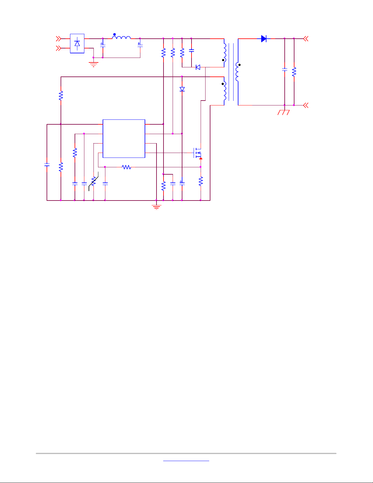
Figure 1. NCP1362 Typical Application Schematic for AC Input Voltage
www.onsemi.com
2
Page 3
NCP1362
V
Vs /
ZCD
Comp
CS
UVLO
V
cc
V
ref_CC
VCC and Logic
Management of
double hiccup
Zero Crossing &
Signal Sampling
CC
Control
V
V
DbleHiccup
POReset
EN_UVP
Sampled V
dd
CC (Reset)
CC (OVP)
out
SS
FB_CC
FB _CV
126% V
V
UVP
UVP_Cmp
EN_UVP
OTA
V
ref_CV1
Peak current
V
DD
I
CS
V
I
CS_EN
Control
1/Kcomp
DD
V
Jitter
LEB 1
V
ILIM
POReset
DbleHiccup
LEB2
Counter
V
CS(Stop )
CS pin Open (VCS>1.2
V) & Short ( V
I
CS_EN
mV) detection is
activated at each startup
POReset
Double_Hiccup_ends
Blanking
QR multi−mode
Valley lockout &
Valley Switching &
VCO management
Control Law
&
Primary Peak
Current Control
OVP_Cmp
4 clk
Counter
OVP
ref_CV1
UVP
DbleHiccup
FB Reset
Max_Ipk reset
Count
Reset
Counter
4 clk
SCP
<50
CS
V
CC(OVP )
OCP
Timer
Reset Timer
FB
UVP
SCP
S
Q
R
OCP
CS pin Fault
Reset
Soft Start
R
S
I
%VBO
SS
BO_EN
BO_DIS
BO_OK
High_Line
UVLO
S
Q
R
POReset
Fault
Q
SS
end
Note:
OVP: Over Voltage Protection
UVP: Under Voltage Protection
OCP : Over Current Protection
SCP: Short Circuit Protection
t
LEB1>tLEB2
FeedForward
V
cc
Clamp
V
fault( OVP)
V
Fault (OTP)
V
fault(EN )
Line
V
V
V
BO (EN)
BO (ON)
HL( on)
BO/LFF
DRV
GND
V
DD
fault(OTP)
I
Fault
fault(clamp)
R
fault(clamp)
V
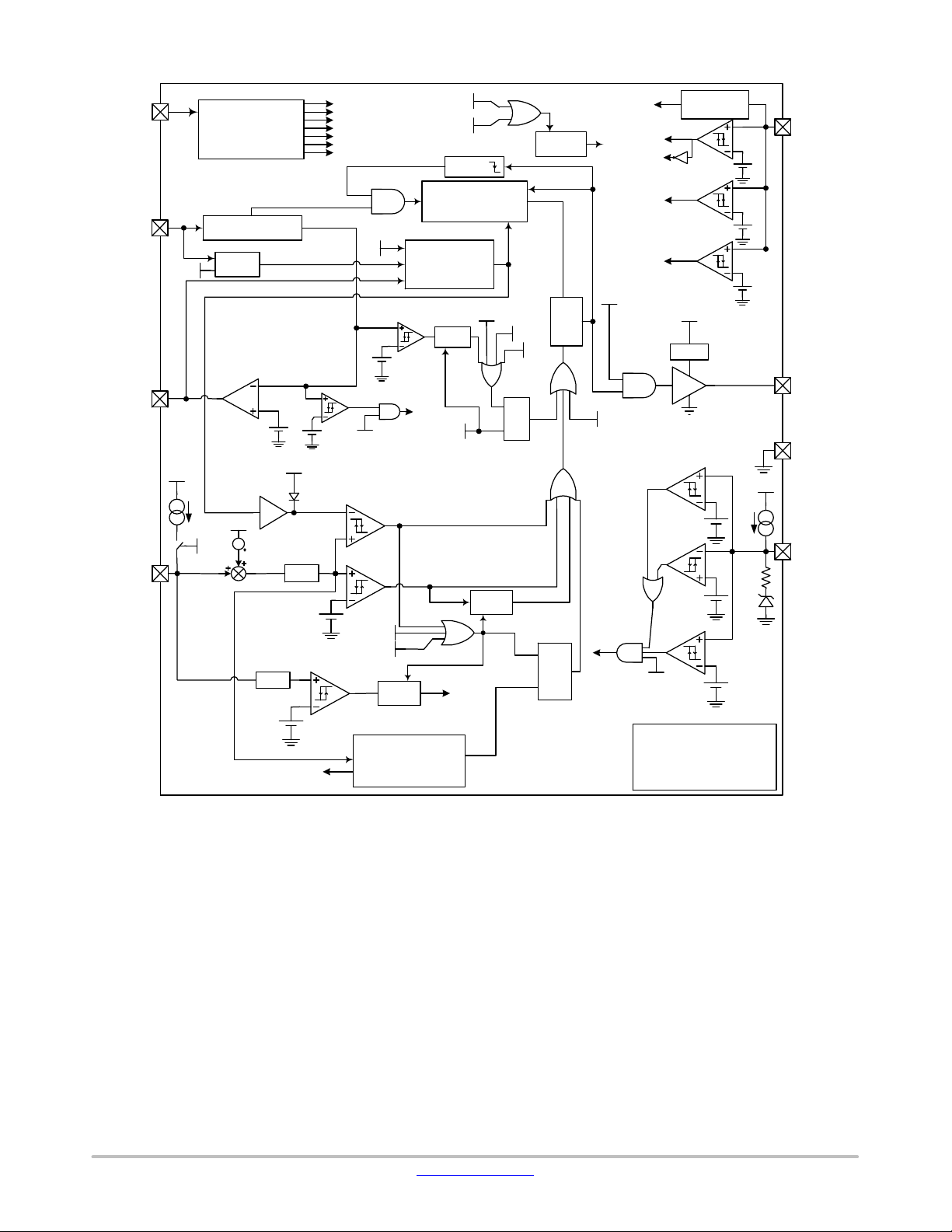
Figure 2. Functional Block Diagram
www.onsemi.com
3
Page 4
NCP1362
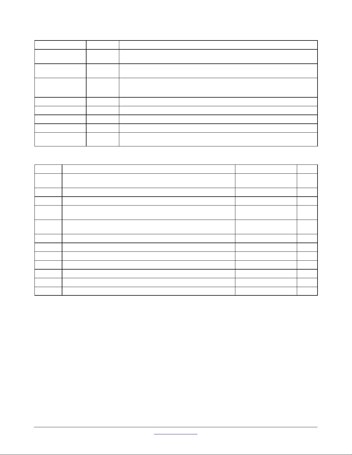
Table 1. PIN FUNCTION DESCRIPTION
Pin Name Function
1 Vs/ZCD Connected to the auxiliary winding; this pin senses the voltage output for the primary regula-
2 Comp This is the error amplifier output. The network connected between this pin and the ground
3 Fault The controller enters in fault mode if the voltage of this pin is pulled above or below the fault
4 CS This pin monitors the primary peak current.
5 DRV The driver’s output to an external MOSFET gate.
6 GND Ground reference.
7 V
CC
8 BO/LFF Detects too low input voltage conditions (Brown−Out). Also voltage pin level is used for build-
Table 2. MAXIMUM RATINGS (Note 1)
Symbol
V
CC(MAX)
I
CC(MAX)
DVCC/Dt
E
V
MAX
I
MAX
V
DRV(MAX)
I
DRV(MAX)
R
θ
T
J(MAX)
Stresses exceeding those listed in the Maximum Ratings table may damage the device. If any of these limits are exceeded, device functionality
should not be assumed, damage may occur and reliability may be affected.
1. This device contains latch−up protection and exceeds 100 mA per JEDEC Standard JESD78.
2. V
DRV
Maximum Power Supply voltage, VCC pin, continuous voltage
Maximum current for V
Maximum slew rate on V
Single Pulse Avalanche Rating 120 mJ
as
Maximum voltage on low power pins (except pins DRV and VCC)
Current range for low power pins (except pins DRV and VCC)
Maximum driver pin voltage, DRV pin, continuous voltage
Maximum current for DRV pin
Thermal Resistance Junction−to−Air, 2.0 oz Printed Circuit Copper Clad 190 °C/W
J−A
Maximum Junction Temperature 150 °C
Operating Temperature Range −40 to +125 °C
Storage Temperature Range −60 to +150 °C
Human Body Model ESD Capability per JEDEC JESD22−A114F 2 kV
Machine Model ESD Capability (All pins except DRV) per JEDEC JESD22−A115C 200 V
Charged−Device Model ESD Capability per JEDEC JESD22−C101E 500 V
is the DRV clamp voltage V
tion and detects the core reset event for the Quasi−Resonant mode of operation.
adjusts the regulation loop bandwidth.
thresholds. A precise pullup current allows direct interface with an NTC thermistor. Fault detection triggers a latch.
This pin is connected to an external auxiliary voltage and supplies the controller.
ing Line FeedForward compensation for improving Constant Current regulation tolerance.
Rating Value Unit
−0.3 to 28
pin
CC
pin during start−up phase +0.4
CC
Internally limited
−0.3, 5.5
−2, +5
DRV(high)
when VCC is higher than V
DRV(high)
. V
is VCC otherwise.
DRV
−0.3, V
(Note 2)
DRV
−300, +500
V
mA
V/ms
V
mA
V
mA
www.onsemi.com
4
Page 5
NCP1362
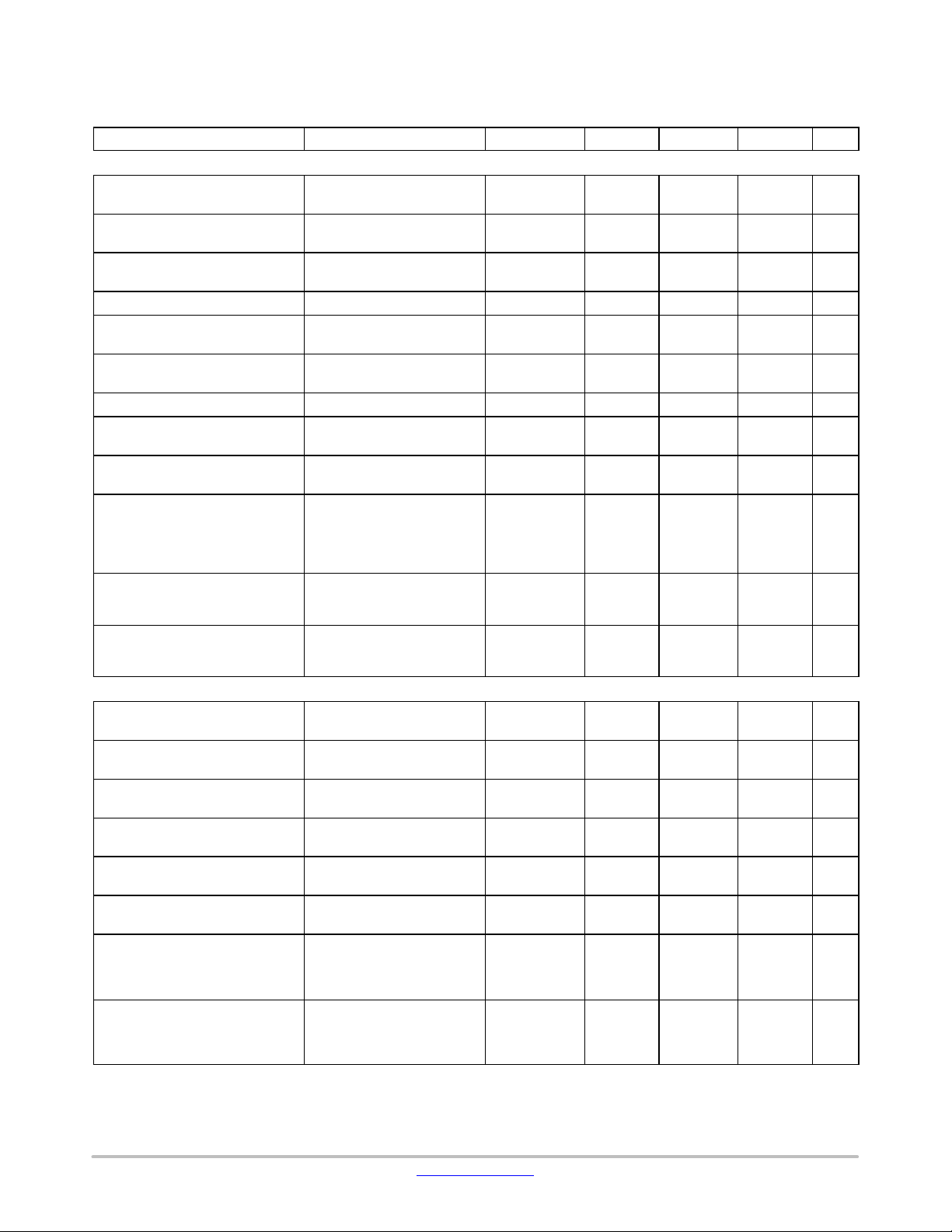
Table 3. ELECTRICAL CHARACTERISTICS
(V
= 12 V, For typical values Tj = 25°C, for min/max values Tj = −40°C to +125°C, Max Tj = 150°C, unless otherwise noted)
CC
Characteristics
SUPPLY SECTION AND VCC MANAGEMENT
Level at which Driving Pulses
V
CC
are Authorized
VCC Level at which Driving Pulses
VCC increasing V
VCC decreasing V
are Stopped
Internal Latch/Logic Reset
Level
Internal Autorecovery Reset Level (Note 4) V
Hysteresis above V
Hiccup in Latch Mode
Hysteresis below V
before Latch Reset
CC(off)
CC(off)
for Fast
Over Voltage Protection Over Voltage threshold V
Start−up Supply Current,
Controller Disabled or Latched
Internal IC Consumption, Steady
State
Internal IC Consumption in
Minimum Frequency Clamp
Internal IC Consumption in Fault
VCC < V
increasing from 0 V
FSW = 65 kHz
C
VCO mode, FSW = f
V
Autorecovery mode I
Mode (after a fault when VCC
decreasing to V
Internal IC Consumption in Fault
Mode (after a fault when V
decreasing to V
CC(off)
CC(off)
)
Latch mode I
CC
)
CURRENT COMPARATOR
Current Sense Voltage
Threshold
V
V
Cycle by Cycle Leading Edge
Blanking Duration
Cycle by Cycle Current Sense
Propagation Delay
Timer Delay before Detecting an
Overload Condition
VCS > (V
DRV turn−off
When CS pin w V
(Note 3)
Threshold for Immediate Fault
Protection Activation
Leading Edge Blanking
Duration for V
Maximum Peak Current Level at
which VCO Takes Over or Frozen
Peak Current
CS(stop)
V
0.6 V < V
(other possible options on
demand)
Minimum Peak Current Level V
V
(other possible options on
demand)
Product parametric performance is indicated in the Electrical Characteristics for the listed test conditions, unless otherwise noted. Product
performance may not be indicated by the Electrical Characteristics if operated under different conditions.
3. The timer can be reset if there are 4 DRV cycles without overload or short circuit conditions.
4. Guaranteed by Design.
Condition Symbol Min Typ Max Unit
16.5 18 19.5 V
6.0 6.5 7.0 V
− 6.25 − V
0.6 − − V
− 0.2 − V
0.15 0.30 0.50 V
24 26 28 V
– 5.4 7.0
– 1.6 2.3 mA
–
–
325
210
– 2.0 2.2 mA
– 1.0 1.2 mA
0.76 0.8 0.84 V
250 320 380 ns
– 50 110 ns
50 70 90 ms
1.10 1.20 1.30 V
− 120 − ns
− 250 − mV
− 65 − mV
= 1 nF
L
Comp
f
VCO(min)
f
VCO(min)
C
= 1 nF
L
Comp
increasing
CS
increasing
CS
increasing
CS
Comp
CC(on)
= GND
= 1 kHz
= 200 Hz
= V
Comp(max)
ILIM
Comp
< 0.2 V
& V
CC
VCO(min)
,
+ 100 mV) to
ILIM
< 1.9 V
,
CC(on)
CC(off)
V
CC(reset)
CC(reset_auto)
V
CC(latch_hyst)
V
CC(reset_hyst)
CC(OVP)
I
CC(start)
I
CC(steady)
I
CC(VCO)
CC(auto)
CC(latch)
V
ILIM
t
LEB1
t
ILIM
T
OCP
V
CS(stop)
t
LEB2
V
CS(VCO)
V
CS(STB)
mA
mA
430
370
www.onsemi.com
5
Page 6

NCP1362
Table 3. ELECTRICAL CHARACTERISTICS
(VCC = 12 V, For typical values Tj = 25°C, for min/max values Tj = −40°C to +125°C, Max Tj = 150°C, unless otherwise noted)
Characteristics UnitMaxTypMinSymbolCondition
REGULATION BLOCK
Internal Voltage Reference for
Constant Current Regulation
Internal Voltage Reference for
Constant Voltage Regulation
TJ = 25°C
−40°C < T
TJ = 25°C
−40°C < T
< 125°C
J
< 125°C
J
Error Amplifier Current
Capability
Error Amplifier Gain G
Error Amplifier Output Voltage Internal offset on Comp pin V
Internal Current Setpoint
Division Ratio
Valley Thresholds
Transition from 1
Transition from 2nd to 3rd Valley
Transition from 3rd to 4th Valley
Transition from 4
Transition from VCO to 4th Valley
Transition from 4th to 3rd Valley
Transition from 3rd to 2nd Valley
Transition from 2nd to 1st Valley
Minimal Difference between any
Two Valleys
Internal Dead Time Generation for
VCO Mode
Internal Dead Time Generation for
VCO Mode
Internal Dead Time Generation for
VCO Mode
Minimum Switching Frequency in
VCO Mode
st
to 2nd Valley
th
Valley to VCO
V
decreasing
Comp
V
decreasing
Comp
V
decreasing
Comp
V
decreasing
Comp
V
increasing
Comp
V
increasing
Comp
V
increasing
Comp
V
increasing
Comp
V
increasing or V
Comp
decreasing
Comp
Entering in VCO when
V
is decreasing and
Comp
crosses V
HVCOD
Leaving VCO mode when
V
is increasing and
Comp
crosses V
HVCOI
When in VCO mode –
1−kHz option
V
= 1.8 V
Comp
V
= 1.4 V
Comp
V
= 0.9 V
Comp
V
< 0.2 V
Comp
V
= GND
Comp
Option 1
Option 2
(other possible options on
demand)
Maximum Switching Frequency
Option 1
Option 2
Option 3
Option 4
Maximum On Time T
DEMAGNETIZATION INPUT – ZERO VOLTAGE DETECTION CIRCUIT and VOLTAGE SENSE
Threshold Voltage V
V
ZCD
V
Hysteresis V
ZCD
decreasing V
ZCD
increasing V
ZCD
Product parametric performance is indicated in the Electrical Characteristics for the listed test conditions, unless otherwise noted. Product
performance may not be indicated by the Electrical Characteristics if operated under different conditions.
3. The timer can be reset if there are 4 DRV cycles without overload or short circuit conditions.
4. Guaranteed by Design.
V
ref_CC
V
ref_CV1
I
EA
EA
Comp(max)
V
Comp(min)
V
Comp(offset)
K
Comp
V
H2D
V
H3D
V
H4D
V
HVCOD
V
HVCOI
V
H4I
V
H3I
V
H2I
DV
H
T
DT(start)
T
DT(ends)
T
DT
f
VCO(MIN)
f
MAX
on(max)
ZCD(TH)
ZCD(HYS)
0.98
0.97
2.450
2.425
1.00
1.00
2.500
2.500
1.02
1.03
2.550
2.575
− ±40 −
150 200 250
−
−
−
4.9
1.1
0
−
−
−
− 4 − –
−
−
−
−
−
−
−
−
2.50
2.30
2.10
1.90
2.50
2.70
2.90
3.10
−
−
−
−
−
−
−
−
176 − − mV
− 1.15 −
− 650 − ns
−
−
−
−
0.8
0.16
−
72
99
127
1.6
11
110
1000
1.0
0.200
No Clamp
80
110
140
−
−
−
−
1.2
0.24
−
88
121
153
32 36 40
25 45 70 mV
15 30 45 mV
V
V
mA
mS
V
V
ms
ms
kHz
kHz
ms
www.onsemi.com
6
Page 7
NCP1362
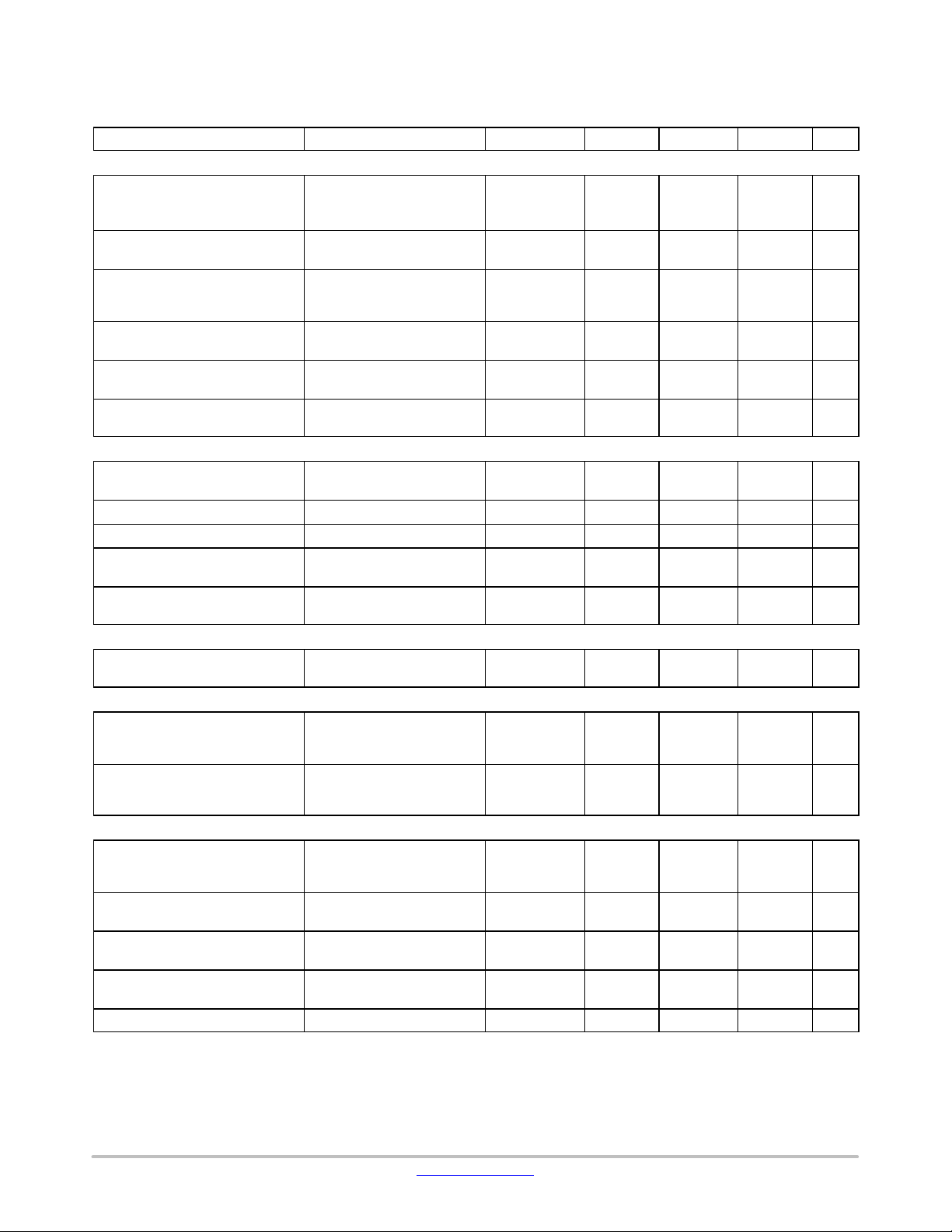
Table 3. ELECTRICAL CHARACTERISTICS
(VCC = 12 V, For typical values Tj = 25°C, for min/max values Tj = −40°C to +125°C, Max Tj = 150°C, unless otherwise noted)
Characteristics UnitMaxTypMinSymbolCondition
DEMAGNETIZATION INPUT – ZERO VOLTAGE DETECTION CIRCUIT and VOLTAGE SENSE
Threshold Voltage for Output
Short Circuit or Aux. Winding
Short Circuit Detection
After t
V
ZCD
BLANK_ZCD
< V
ZCD(short)
if
V
ZCD(short)
30 50 75 mV
Delay after On−time that the
V
/ZCD is still Pulled to Ground
S
Blanking Delay after On−time
(V
/ZCD Pin is Disconnected from
S
the Internal Circuitry)
Timeout after Last
Demagnetization Transition
Input Leakage Current VCC > V
Delay from Valley Detection to
DRV Low
When V
Comp
When V
Comp
When V
Comp
When V
Comp
CC(on) VZCD
DRV is low
> 1.7 V
< 1.7 V
> 1.7 V
< 1.7 V
= 4 V,
t
short_ZCD
t
BLANK_ZCD
t
out
I
ZCD
t
ZCD_delay
−
−
−
−
0.750
0.350
1.450
0.750
−
−
−
−
4.0 4.5 5.0
− − 0.1
− 290 − ns
ms
ms
ms
mA
DRIVE OUTPUT − GATE DRIVE
Drive resistance
DRV Sink − VCC = 8 V
DRV Source − V
Rise time C
Fall time C
= 1 nF, from 10% to 90% t
DRV
= 1 nF, from 90% to 10% t
DRV
DRV Low voltage VCC = V
= 220 pF, R
DRV High voltage VCC = V
= 220 pF, R
CC(off)
DRV
CC(OVP)
DRV
= 8 V
CC
+ 0.2 V, C
= 33 kW
− 0.2 V, C
= 33 kW
DRV
DRV
R
SNK
R
SRC
V
DRV(low)
V
DRV(high)
−
−
r
f
− 45 85 ns
− 30 65 ns
10
8
−
W
−
6.0 − − V
− 12.0 13.0 V
SOFT START
Internal Fixed Soft Start Duration
Current Sense peak current
rising from V
CS(VCO)
to V
ILIM
t
SS
3 4 5 ms
JITTERING
Frequency of the Jittering CS Pin
Source Current
Option 1
(other possible options on
f
jitter
1.2 1.5 1.8 kHz
demand)
Peak Jitter Voltage Added to
PWM Comparator
Option 1
(other possible options on
V
jittter
− 60 − mV
demand)
BROWN−OUT & LINE FEED FORWARD
Brown−out Function is Disabled
below this Level (before the 1
st
V
BO(en)
80 100 120 mV
DRV pulse only)
Pull−down Current Source on BO
Pin for Open Detection
Brown−out Level at which the
Controller Starts Pulsing
Brown−out Level at which the
Controller Stops Pulsing
Brown−out Filter Time t
V
BO(on)
V
BO(off)
I
BO
− 300 − nA
0.75 0.80 0.85 V
0.65 0.70 0.75 V
BO
− 50 −
ms
Product parametric performance is indicated in the Electrical Characteristics for the listed test conditions, unless otherwise noted. Product
performance may not be indicated by the Electrical Characteristics if operated under different conditions.
3. The timer can be reset if there are 4 DRV cycles without overload or short circuit conditions.
4. Guaranteed by Design.
www.onsemi.com
7
Page 8
NCP1362
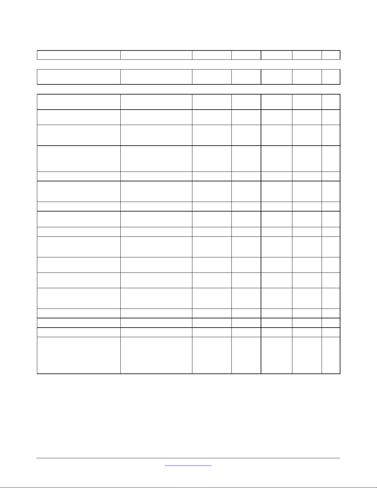
Table 3. ELECTRICAL CHARACTERISTICS
(VCC = 12 V, For typical values Tj = 25°C, for min/max values Tj = −40°C to +125°C, Max Tj = 150°C, unless otherwise noted)
Characteristics UnitMaxTypMinSymbolCondition
BROWN−OUT & LINE FEED FORWARD
Line Feed Forward Compensation
Gain
FAULT PROTECTION
Controller Thermal Shutdown
Device switching
(F
∼ 65 kHz) – Tj rising
SW
Thermal Shutdown Hysteresis Device switching
(F
∼ 65 kHz) − Tj falling
SW
Fault Level Detection for OVP Internal sampled V
increasing
V
= V
OVP
ref_CV1
Fault Level Detection for UVP →
Double Hiccup Autorecovery
Internal sampled V
decreasing
out
+ 26%
out
(UVP detection is disabled during
T
EN_UVP
)
Blanking Time for UVP Detection Starting after the Soft start T
Pull−up Current Source on CS Pin
for Open or Short Circuit Detec-
When VCS > V
CS_min
tion
CS Pin Open Detection CS pin open V
K
LFF
T
SHTDN(on)
T
SHTDN(off)
V
OVP
V
UVP
EN_UVP
I
CS
CS(open)
16 20 24
− 150 − °C
− 120 − °C
2.95 3.15 3.35 V
1.40 1.50 1.60 V
− 36 − ms
− 60 −
− 1.2 − V
mA/
V
mA
CS Pin Short Detection V
CS pin Short Detection Timer (Note 4) T
Fault Pin is Disabled below this
Level (before the 1
st
DRV pulse
V
CS_min
CS_short
Fault(EN)
− 50 75 mV
− 3 −
ms
80 100 120 mV
only)
Overvoltage Protection (OVP)
Threshold
Overtemperature Protection
(OTP) Threshold
OTP Pull−up Current Source V
Fault Input Clamp Voltage I
Fault Input Clamp Voltage I
Fault Filter Time t
Number of Drive Cycle before
Latch Confirmation
V
increasing V
Fault
V
decreasing V
Fault
= 0 V
Fault
T
= 25°C
j
= 110°C
T
j
= 0 mA (V
Fault
= 1 mA V
Fault
V
= V
Comp
V
CS
or Internal rebuilded
V
out
or 0.40 V < V
or V
> V
CS(stop)
> V
OVP
ZCD(short)
Comp(max)
Fault
Fault
< 3.00 V
= open) V
,
Fault(OVP)
Fault(OTP)
I
Fault(OTP)
I
Fault(OTP_110)
Fault(clamp)0
Fault(clamp)1
Fault(filter)
t
latch(count)
2.79 3.00 3.21 V
0.38 0.40 0.42 V
42.5
42.9
45.0
45.0
47.5
46.5
1.10 1.35 1.60 V
2.2 2.7 3.2 V
− 2 −
− 4 − −
mA
ms
Product parametric performance is indicated in the Electrical Characteristics for the listed test conditions, unless otherwise noted. Product
performance may not be indicated by the Electrical Characteristics if operated under different conditions.
3. The timer can be reset if there are 4 DRV cycles without overload or short circuit conditions.
4. Guaranteed by Design.
www.onsemi.com
8
Page 9
NCP1362
)
)
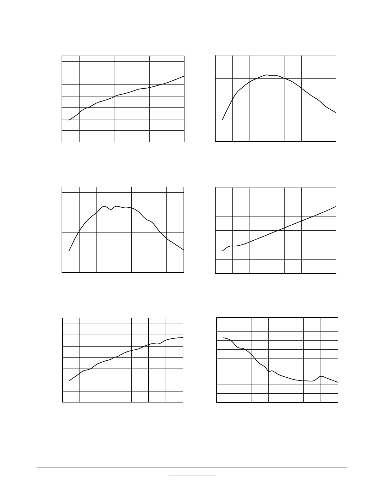
TYPICAL CHARACTERISTICS
18.09
18.07
18.05
(V)
18.03
CC(on)
18.01
V
17.99
17.97
17.95
−50 −25 0 25 50 75 100 125
TEMPERATURE (5C)
(V)
CC(reset)
V
6.292
6.287
6.282
6.277
6.272
Figure 3. V
vs. Junction Temperature Figure 4. V
CC(on)
6.59
6.585
6.58
(V)
6.575
CC(off)
V
6.57
6.565
6.56
−50 −25 0 25 50 75 100 125
TEMPERATURE (5C)
vs. Junction Temperature
CC(off)
5.2
4.7
4.2
(mA)
3.7
CC(start)
I
3.2
6.267
6.262
−50 −25 0 25 50 75 100 125
TEMPERATURE (5C)
Figure 5. V
0.808
0.806
0.804
(V)
0.802
ILIM
V
0.8
0.798
0.796
0.794
−50 −25 0 25 50 75 100 125
CC(reset
vs. Junction Temperature Figure 6. I
TEMPERATURE (5C)
Figure 7. V
vs. Junction Temperature Figure 8. t
ILIM
2.7
2.2
−50 −25 0 25 50 75 100 125
TEMPERATURE (5C)
vs. Junction Temperature
(ns)
LEB1
t
CC(start
316.5
316
315.5
315
314.5
314
313.5
313
312.5
312
−50 −25 0 25 50 75 100 125
TEMPERATURE (5C)
vs. Junction Temperature
LEB1
www.onsemi.com
9
Page 10
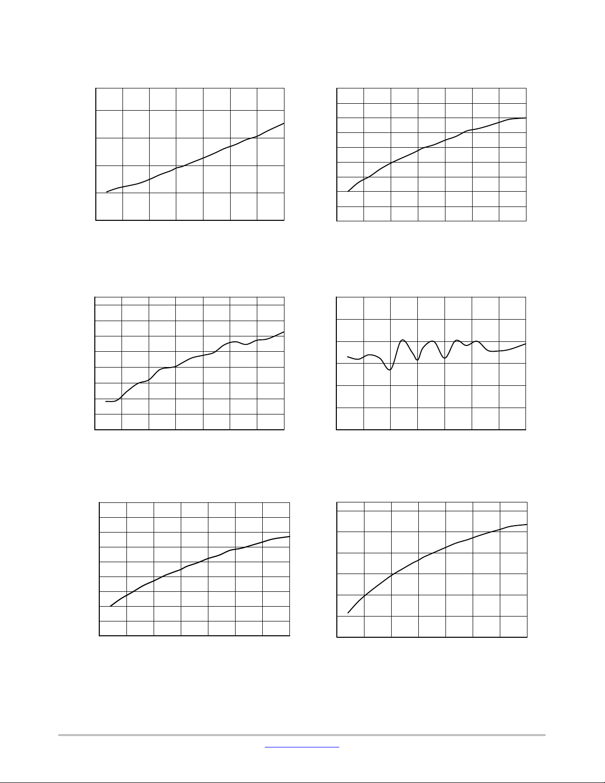
TYPICAL CHARACTERISTICS (Continued)
)
)
74
69
(ns)
64
ILIM
t
59
54
−50 −25 0 25 50 75 100 125
TEMPERATURE (5C)
NCP1362
1.209
1.207
1.205
1.203
(V)
1.201
1.199
CS(stop)
V
1.197
1.195
1.193
1.191
−50 −25 0 25 50 75 100 125
TEMPERATURE (5C)
Figure 9. t
254
253
252
251
(mV )
250
CS(VCO)
249
V
248
247
246
−50 −25 0 25 50 75 100 125
vs. Junction Temperature Figure 10. V
ILIM
TEMPERATURE (5C)
Figure 11. V
1.013
1.011
1.009
1.007
(V)
1.005
1.003
ref_CC
V
1.001
0.999
0.997
0.995
−50 −25 0 25 50 75 100 125
CC(VCO
vs. Junction Temperature Figure 12. V
TEMPERATURE (5C)
vs. Junction Temperature
CS(stop)
70
69.5
69
(mV )
68.5
CS(STB)
V
68
67.5
67
−50 −25 0 25 50 75 100 125
TEMPERATURE (5C)
vs. Junction Temperature
CS(STB
2.51
2.505
2.5
(V)
2.495
ref_CV1
V
2.49
2.485
2.48
−50 −25 0 25 50 75 100 125
TEMPERATURE (5C)
Figure 13. V
vs. Junction Temperature Figure 14. V
ref CC
www.onsemi.com
10
vs. Junction Temperature
ref CV1
Page 11
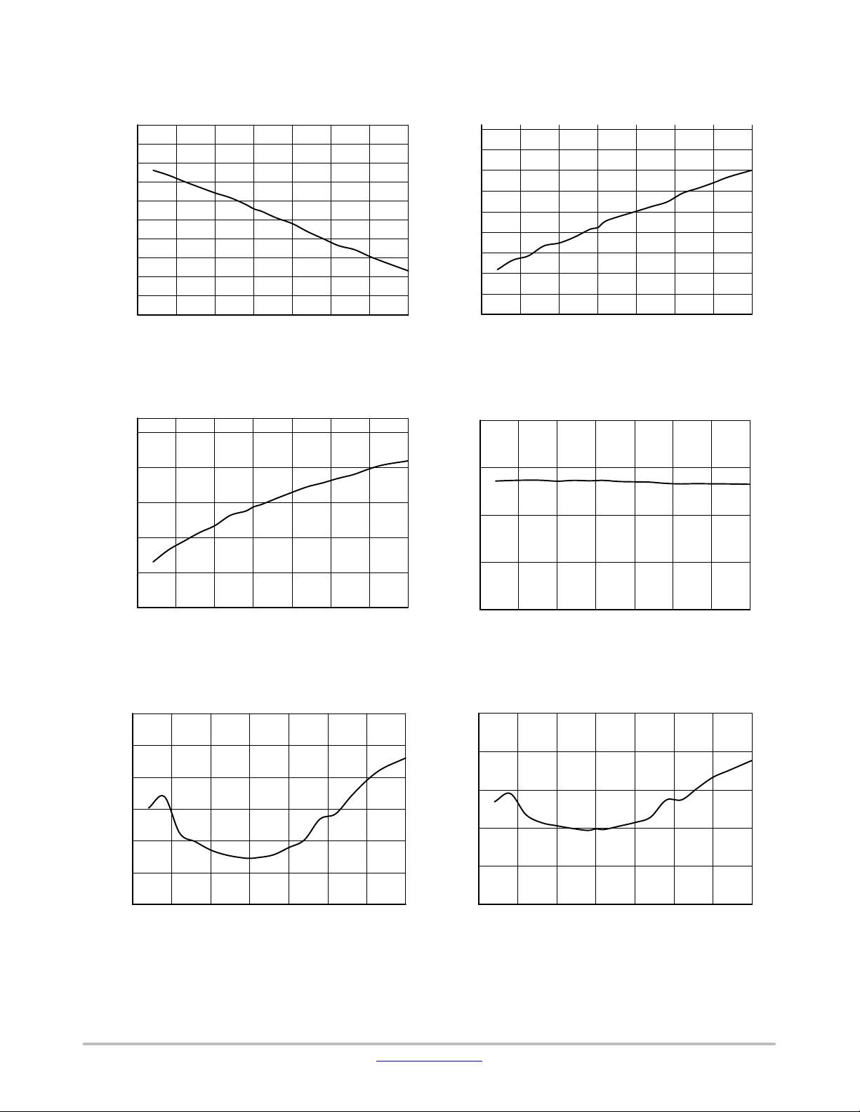
NCP1362
)
TYPICAL CHARACTERISTICS (Continued)
48
47.5
47
46.5
46
(mV)
45.5
45
ZCD(TH)
V
44.5
44
43.5
43
−50 −25 0 25 50 75 100 125
TEMPERATURE (5C)
Figure 15. V
3.17
3.16
3.15
(V)
OVP
V
3.14
ZCD(TH)
vs. Junction Temperature Figure 16. V
57.7
57.2
56.7
56.2
(mV)
55.7
55.2
54.7
ZCD(short)
V
54.2
53.7
53.2
−50 −25 0 25 50 75 100 125
TEMPERATURE (5C)
ZCD(short)
1.56
1.555
vs. Junction Temperature
(V)
1.55
UVP
V
3.13
3.12
−50 −25 0 25 50 75 100 125
TEMPERATURE (5C)
Figure 17. V
36.32
36.27
36.22
(ms)
36.17
EN_UVP
T
36.12
36.07
36.02
−50 −25 0 25 50 75 100 125
vs. Junction Temperature Figure 18. V
OVP
TEMPERATURE (5C)
Figure 19. T
vs. Junction Temperature Figure 20. V
EN UVP
(V)
BO(on)
V
1.545
1.54
-50 -25 0 25 50 75 100 125
TEMPERATURE (5C)
vs. Junction Temperature
UVP
0.84
0.839
0.838
0.837
0.836
0.835
−50 −25 0 25 50 75 100 125
TEMPERATURE (5C)
vs. Junction Temperature
BO(on
www.onsemi.com
11
Page 12
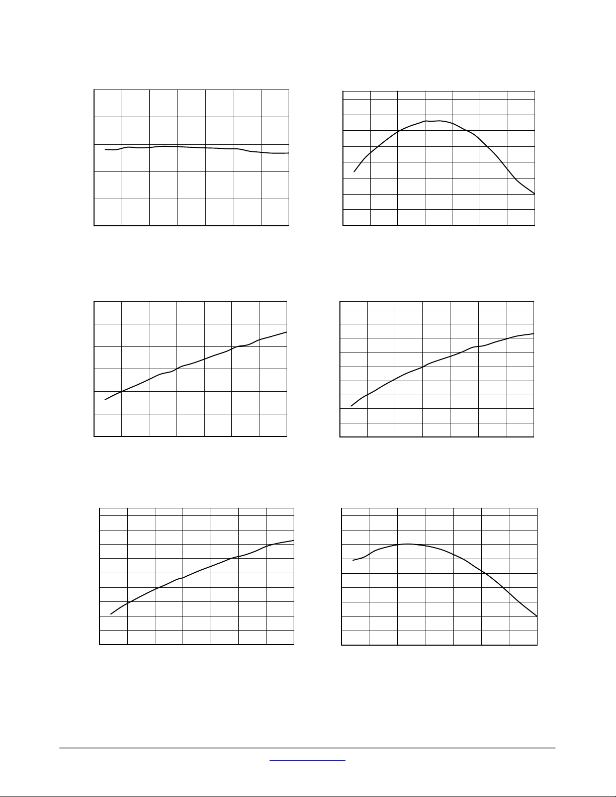
NCP1362
V
(V)
)
)
)
)
TYPICAL CHARACTERISTICS (Continued)
0.695
0.693
0.691
0.689
BO(off)
0.687
0.685
−50 −25 0 25 50 75 100 125
TEMPERATURE (5C)
Figure 21. V
106.5
105.5
104.5
vs. Junction Temperature Figure 22. K
BO(off)
(mV)
103.5
Fault(EN)
102.5
V
101.5
100.5
-50 -25 0 25 50 75 100 125
TEMPERATURE (5C)
Figure 23. V
Fault(EN
vs. Junction Temperature Figure 24. V
21.63
21.61
21.59
21.57
(mA/V)
21.55
LFF
K
21.53
21.51
21.49
21.47
−50 −25 0 25 50 75 100 125
TEMPERATURE (5C)
vs. Junction Temperature
LFF
3.011
3.006
3.001
2.996
(V)
2.991
2.986
Fault(OVP)
2.981
V
2.976
2.971
2.966
−50 −25 0 25 50 75 100 125
TEMPERATURE (5C)
Fault(OVP
vs. Junction Temperature
0.407
0.406
0.405
0.404
(V)
0.403
0.402
Fault(OTP)
0.401
V
0.4
0.399
0.398
−50 −25 0 25 50 75 100 125
TEMPERATURE (5C)
Figure 25. V
Fault(OTP
vs. Junction Temperature Figure 26. I
45.3
45.2
45.1
45
(mA)
44.9
44.8
Fault(OTP)
44.7
I
44.6
44.5
44.4
−50 −25 0 25 50 75 100 125
www.onsemi.com
12
TEMPERATURE (5C)
Fault(OTP
vs. Junction Temperature
Page 13

Table 4. FAULT MODES
Event Timer Protection Next Device Status Release to Normal Operation Mode
Overcurrent
V
> V
CS
ILIM
Winding Short
V
> V
CS
CS(stop)
CS Pin Fault:
Short & Open
ZCD Short
V
ZCD
t
BLANK_ZCD
< V
ZCD(short)
time
after
Low Supply
V
< V
CC
CC(off)
High Supply
V
> V
CC
CC(ovp)
OVP: V
UVP: V
when V
Internal V
out
Internal V
out
out
out
> 126% V
< 60% V
is Decreasing Only
out
ref_CV1
ref_CV1
,
Internal TSD
NOTE: Latching off protection available upon request.
OCP Timer Double Hiccup − Resume to normal operation: if 4 pulses from
4 Consecutive Pulses
with V
CS
> V
CS(stop)
Before Start−up
Immediate
4 Consecutive Pulses Double Hiccup Resume operation after Double Hiccup
10−ms Timer
10−ms Timer
4 Consecutive Pulses Double Hiccup Resume operation after Double Hiccup
4 Consecutive Pulses Double Hiccup Resume operation after Double Hiccup
10−ms Timer
NCP1362
FB Reset & then Reset timer
− Resume operation after Double Hiccup
Double Hiccup Resume operation after Double Hiccup
Double Hiccup Resume operation after Double Hiccup
Simple Hiccup Resume operation after Simple Hiccup
Double Hiccup Resume operation after Double Hiccup
Double Hiccup Resume operation after Double Hiccup &
T < (T
SHTDN(off)
)
www.onsemi.com
13
Page 14

NCP1362
APPLICATION INFORMATION
The NCP1362 is a flyback power supply controller
providing a means to implement primary side constant−
current regulation and secondary side constant−voltage
regulation. NCP1362 implements a current−mode
architecture operating in quasi−resonant mode. The
controller prevents valley−jumping instability and steadily
locks out in a selected valley as the power demand goes
down. As long as the controller is able to detect a valley, the
new cycle or the following drive remains in a valley. Thanks
to a dedicated valley detection circuitry operating at any line
and load conditions, the power supply efficiency will always
be optimized. In order to prevent any high switching
frequency two frequency clamp options are available.
• Quasi−Resonance Current−mode Operation:
implementing quasi−resonance operation in peak
current−mode control optimizes the efficiency by
switching in the valley of the MOSFET drain−source
voltage. Thanks to a proprietary circuitry, the controller
locks−out in a selected valley and remains locked until
the input voltage significantly changes. Only the four
first valleys could be locked out. When the load current
diminishes, valley switching mode of operation is kept
but without valley lock−out. Valley−switching
operation across the entire input/output conditions
brings efficiency improvement and lets the designer
build higher−density converters.
• Frequency Clamp: As the frequency is not fixed and
dependent on the line, load and transformer
specifications, it is important to prevent switching
frequency runaway for applications requiring maximum
switching frequencies up to 90 kHz or 130 kHz. Three
frequency clamp options at 80 kHz, 110 kHz or
140 kHz are available for this purpose. In case
frequency clamp is not needed, a specific version of the
NCP1362 exists in which the clamp is deactivated.
• Primary Side Constant Current Regulation: NCP1362
controls and regulates the output current at a constant
level regardless of the input and output voltage
conditions. This function offers tight over power
protection by estimating and limiting the maximum
output current from the primary side, without any
particular sensor.
V
OUT
V
NOM
0
Figure 27. Constant−Voltage & Constant−Current
CV Mode
Mode
I
NOM
CC Mode
I
OUT
• Soft−Start: 4−ms internal fixed soft start guarantees
a peak current starting from zero to its nominal value
with smooth transition in order to prevent any
overstress on the power components at each startup.
• Cycle−by−Cycle Peak Current Limit: If the max peak
current reaches the V
level, the over current
ILIM
protection timer is enabled and starts counting. If the
overload lasts T
delay, then the fault is detected and
OCP
the controller stops immediately driving the power
MOSFET. The controller enters in a double hiccup
mode before autorecovering with a new startup cycle.
• V
Over Voltage Protection: If the V
CC
reaches the V
CC(OVP)
threshold the controller enters in
CC
voltage
fault mode. Thus it stops driving pulse on DRV pin.
The part enters in double hiccup mode before resuming
operation.
• Winding Short−Circuit Protection: An additional
comparator senses the CS signal and stops the
controller if V
LEB: t
LEB2
reaches V
CS
+ 50% (after a reduced
ILIM
). Short circuit protection is enabled only if
4 consecutive pulses reach SCP level. This small
counter prevents any false triggering of short circuit
protection during surge test for instance. This fault is
detected and operations will be resumed like in a case
Over Voltage Protection.
of V
CC
• V
Over Voltage Protection: if the internally−built
out
output voltage becomes higher than V
(V
+ 26%) a fault is detected. This fault is
ref_CV1
OVP
level
detected and operations are resumed like in the
VCC Over Voltage Protection case.
• V
Under Voltage Protection: After each circuit power
out
on sequence, V
the startup timer T
UVP detection is enabled only after
out
. This timer ensures that the
EN_UVP
power supply is able to fuel the output capacitor before
checking the output voltage in on target. After this
startup blanking time, UVP detection is enabled and
monitors the Output voltage level. When the power
supply is running in constant−current mode and when
the output voltage falls below V
level, the controller
UVP
stops sending drive pulses and enters a double hiccup
mode before resuming operations.
• V
/ZCD Pin Short Protection: at the beginning of each
S
off−time period, the V
/ZCD pin is tested to check
S
whether it is shorted or left open. In case a fault is
detected, the controller enters in a double hiccup mode
before resuming operations.
• EMI Jittering: a low−frequency triangular voltage
waveform is added to the CS pin. This helps spreading
out energy in conducted noise analysis. Jittering is
disabled in frequency foldback mode.
• Frequency Foldback: In frequency foldback mode,
the system reduces the switching frequency by adding
some dead−time after the 4
th
valley is detected.
www.onsemi.com
14
Page 15

NCP1362
The controller will still run in valley switching mode
even when the FF is enabled.
• Temperature Shutdown: if the junction temperature
reaches the T
power MOSFET until the junction temperature
decreases to T
after a double hiccup mode.
level, the controller stop driving the
SHTDN
SHTDN(off)
, then the operation is resumed
• Brown−Out Detection: BO pin monitors bulk voltage
level via resistive divider and thus assures that the
application is working only for designed bulk voltages.
When BO pin is grounded before start−up
< V
(V
BO
dynamic frequency clamp are disabled.
), Brown−Out, Line FeedForward and
BO(en)
• Line FeedForward: By monitoring the voltage
available on BO pin it is possible to create a line
feedforward compensation in order to improve the
constant current accuracy.
• Fault Input: the NCP1362 includes a dedicated fault
input. It can be used to sense an overvoltage condition
and latch off the controller by pulling up the pin above
the upper fault threshold, V
Fault(OVP)
The controller is also disabled if the Fault pin voltage,
, is pulled below the lower fault threshold,
V
Fault
V
Fault(OTP)
, typically 0.4 V. The lower threshold is
normally used for detecting an overtemperature fault
(by the means of an NTC). If this pin is grounded
before start−up, then its associated feature are disabled.
, typically 3.0 V.
www.onsemi.com
15
Page 16
DETAILED APPLICATION INFORMATION
NCP1362
Start−up Sequence
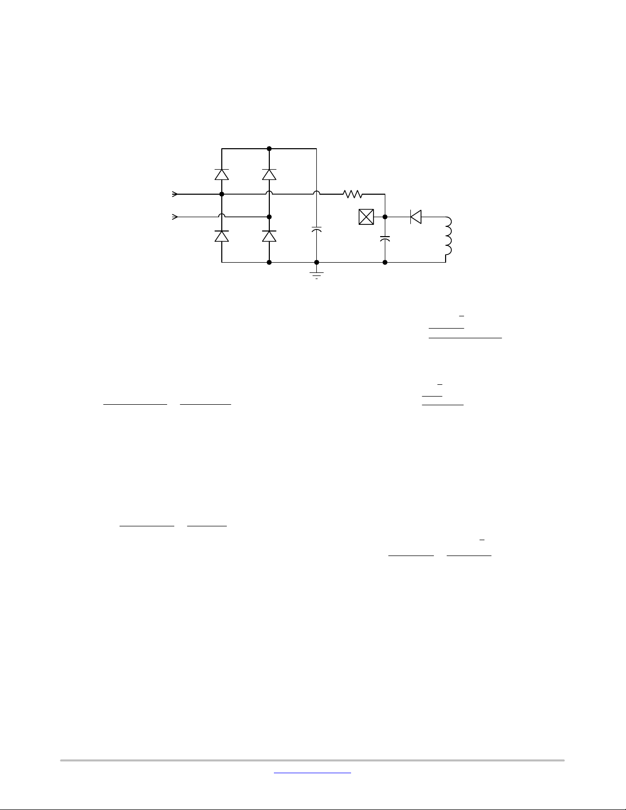
The NCP1362 start−up voltage is made purposely high to
permit large energy storage in a small V
capacitor value.
CC
This helps operate with a small start−up current which,
together with a small V
capacitor, will not hamper the
CC
Input
Mains
start−up time. To further reduce the standby power, the
start−up current of the controller is extremely low (see
I
CC(start)
). The start−up resistor can therefore be connected
to the bulk capacitor or directly to the mains input voltage to
further reduce the power dissipation.
R
Start−up
V
CC
C
bulk
C
VCC
Aux.
Winding
Figure 28. The Startup Resistor can be Connected to the Input Mains for Further Power Dissipation Reduction
The first step starts with the calculation of the needed V
CC
capacitor which will supply the controller when it operates
until the auxiliary winding takes over. Experience shows
that this time t
consider we need at least an energy reservoir for a t
10 ms, the V
C
w
V
CC
can be between 5 ms and 20 ms. If we
1
capacitor must be larger than:
CC
I
V
CC(on)
CC
t
* V
1
CC(off)
1.6 m 10 m
w
18 * 6.5
w 1.4 mF
time of
1
(eq. 1)
Let us select a 1.5 mF capacitor at first and experiments in
the laboratory will let us know if we were too optimistic for
the time t
evaluate the charging current we need to bring the V
voltage from 0 V to the V
. The VCC capacitor being known, we can now
1
of the IC. This current has
CC(on)
CC
to be selected to ensure a start−up at the lowest mains (85 V
rms) to be less than 3 s (2.5 s for design margin):
V
C
I
charge
CC(on)
w
t
start−up
If we account for the I
Vcc
w
CC(start)
18 1.5 m
2.5
w 11 mA
(eq. 2)
= 6.3 mA (maximum) that
will flow inside the controller, then the total charging current
I
CVcc,min
+
To make sure this current is always greater than 16 mA,
then the minimum value for R
85 2
R
start−up
v
This calculation is purely theoretical, considering
a constant charging current. In reality, the take over time can
be shorter (or longer!) and it can lead to a reduction of the
V
capacitor. Thus, a decrease in charging current and an
CC
increase of the start−up resistor can be experimentally
tested, for the benefit of standby power. Laboratory
experiments on the prototype are thus mandatory to fine tune
the converter. If we chose the 1.2−MW resistor as suggested
by Eq. 4, the dissipated power at high line amounts to:
2
V
P
R
start−up,max
[
ac,peak
4 R
start−up
V
ac,rms
Ǹ
p
17.3 m
[
Ǹ
2
* V
p
R
start−up
can be extracted:
start−up
* 18
v 1.17 MW
Ǹ
ǒ
230 2
4 1.1 M
CC(on)
2
Ǔ
[ 24 mW
delivered by the start−up resistor must be 17.3 mA. If we
connect the start−up network to the mains (half−wave
connection then), we know that the average current flowing
into this start−up resistor will be the smallest when V
reaches the V
of the controller:
CC(on)
CC
Primary Side Regulation: Constant Current Operation
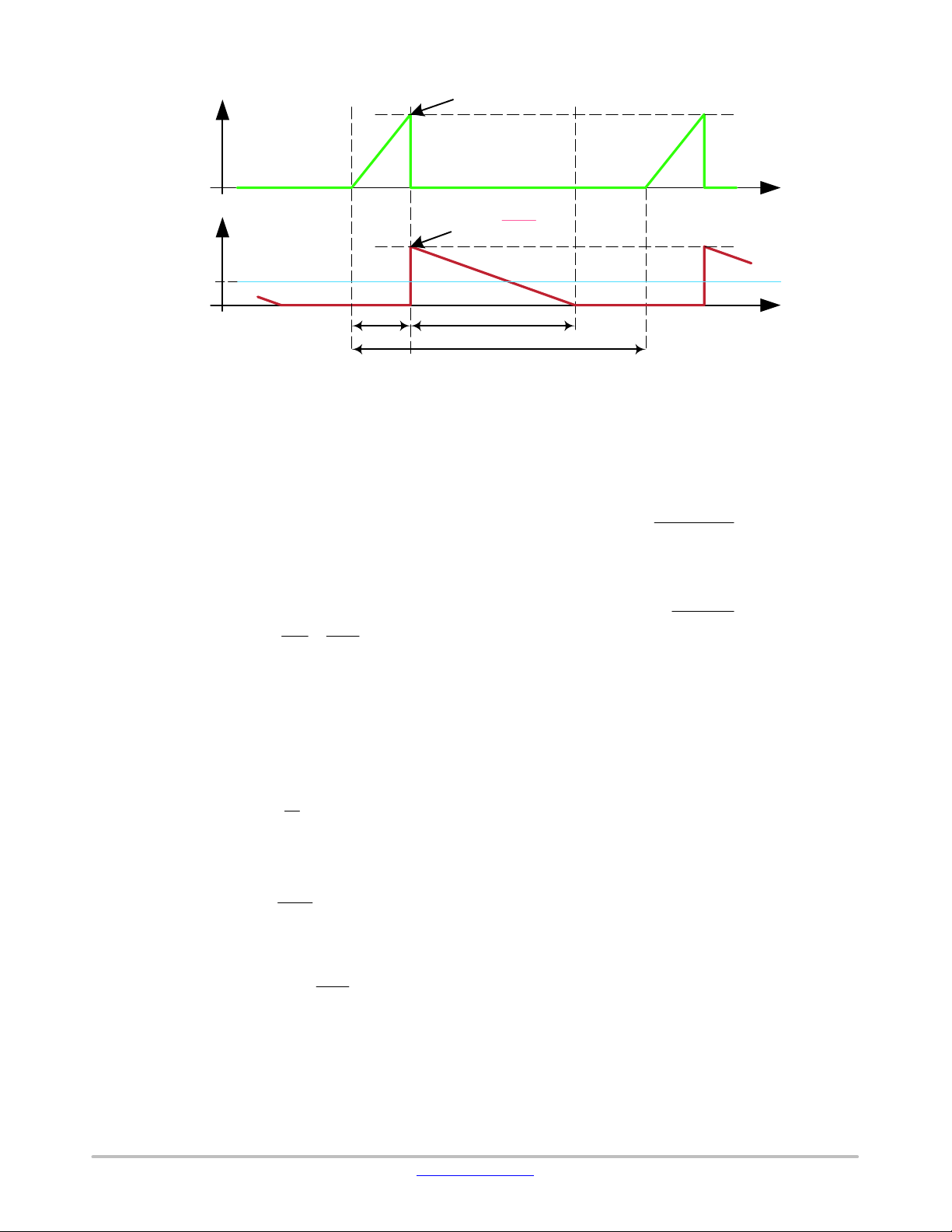
Figure 29 portrays idealized primary and secondary
transformer currents of a flyback converter operating in
Discontinuous Conduction Mode (DCM).
(eq. 3)
(eq. 4)
(eq. 5)
www.onsemi.com
16
Page 17
NCP1362
Ip(t)
(t), I
I
s
OUT
= <I
I
OUT
When the primary power MOSFET is turned on, the
primary current is illustrated by the green curve of
Figure 29. When the power MOSFET is turned off the
primary side current drops to zero and the current into the
secondary winding immediately rises to its peak value equal
to the primary peak current divided by the primary to
secondary turns ratio. This is an ideal situation in which the
leakage inductance action is neglected.
The output current delivered to the load is equal to the
average value of the secondary winding current, thus we can
write:
Where:
• t
is the switching period
SW
• t
• N
is the demagnetizing time of the transformer
demag
is the secondary to primary turns ratio, where
PS
& NS are respectively the transformer primary and
N
P
secondary turns:
• I
is the magnetizing peak current sensed across the
p,pk
sense resistor on CS pin:
Internal constant current regulation block is building the
constant current feedback information as follow:
s(t)
>
t
on
Figure 29. Primary and Secondary Transformer Current Waveforms
t
I
demag
I
+ 〈i
sec
out
I
p,pk
V
FB_CC
(t)〉 +
Nps+
+
+ V
2N
N
N
V
R
ref_CC
p,pk
ps
s
p
CS
sense
t
sw
t
SW
t
demag
(eq. 6)
(eq. 7)
(eq. 8)
(eq. 9)
,pIpk
I
t
demag
,,ppk
ps
t
sw
IN=
spk
As the controller monitors the primary peak current via
the sense resistor and due to the internal current setpoint
divider (K
) between the CS pin and the internal
comp
feedback information, the output current could be written as
follow:
V
+
8Nps R
ref_CC
sense
I
out
The output current value is set by choosing the sense
resistor value:
V
+
8Nps I
ref_CC
out
R
sense
Primary Side Regulation: Constant Voltage Operation
In primary side constant voltage regulation, the output
voltage is sensed via the auxiliary winding. During the
on−time period, the energy is stored in the transformer gap.
During the off−time this energy stored in the transformer is
delivered to the secondary and auxiliary windings.
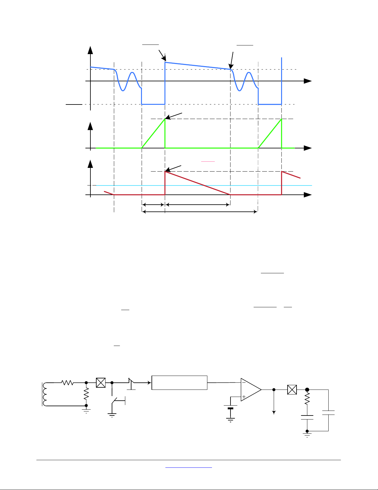
As illustrated by Figure 30, when the transformer energy
is delivered to the secondary, the auxiliary voltage sums the
output voltage scaled by the auxiliary and secondary turns
ratios and the secondary forward diode voltage. This
secondary forward diode voltage could be split in two
elements: the first part is the forward voltage of the diode
(V
), and the second is related to the dynamic resistance of
f
the diode multiplied by secondary current (R
Where this second term will be dependant of the load and
line conditions.
time
time
(eq. 10)
(eq. 11)
y IS(t)).
D
www.onsemi.com
17
Page 18
NCP1362
VN*
I
OUT
IN
N
= <I
0V
pa
ps
s(t)
I
s
>
V
AUX
Ip(t)
(t), I
(t)
OUT
N
N
pa
+
()
sec
ps
,pIpk
I
t
demag
,,ppk
ps
t
sw
IN=
spk
t
on
VVI
out f
V
out
N
N
pa
ps
time
time
time
Figure 30. Typical Idealized Waveforms of a Flyback Transformer in DCM
To reach an accurate primary−side constant−voltage
regulation, the controller detects the end of the
demagnetization time and precisely samples output voltage
level seen on the auxiliary winding. As this moment
coincides with the secondary−side current equal to zero, the
diode forward voltage drop becomes independent from the
loading conditions.
Thus when the secondary current I
(t) reaches zero
s
ampere, the auxiliary is sensed:
N
V
+ V
aux
out
pa
N
ps
(eq. 12)
Where: Npa is the auxiliary to primary turns ratio, where N
& Na are respectively the primary and auxiliary turns:
N
Auxiliary
Npa+
Vs / ZCD
R
s1
R
s2
a
N
p
t
Blank_ZCD
t
Short_ZCD
(eq. 13)
Zero Crossing &
Signal Sampling
Figure 31 illustrates how the constant voltage feedback
has been built. The auxiliary winding voltage must be scaled
down via the resistor divider to V
ref_CV1
building the constant voltage feedback error.
R
V
ref_CV1
+
Rs1) R
s2
V
aux
s2
By inserting Eg. 12 into Eq. 14 we obtain the following
equation:
R
V
ref_CV1
Once the sampled V
p
terminal of the operational transconductance amplifier
s2
+
Rs1) R
is applied to the negative input
out
N
pa
V
N
ps
s2
(OTA) and compared to the internal voltage reference an
adequate voltage feedback is built. The OTA output being
pinned out, it is possible to compensate the converter and
adjust step load response to what the project requires.
Sampled V
V
ref_CV1
out
OTA
Comp
FB_CV
level before
(eq. 14)
out
(eq. 15)
R1
C2
C1
Figure 31. Constant Voltage Feedback Arrangement
www.onsemi.com
18
Page 19
NCP1362
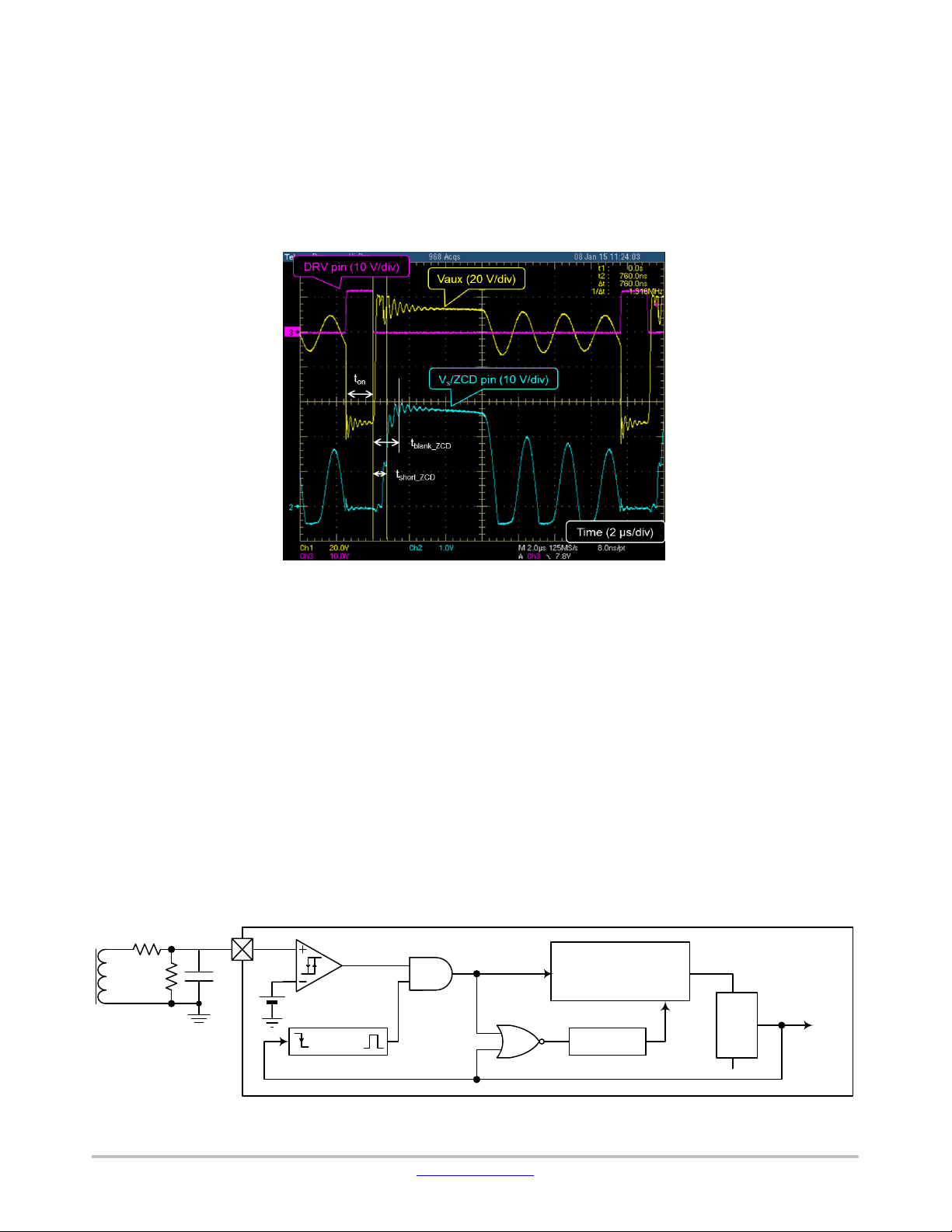
When the power MOSFET is released at the end of the on
time, because of the transformer leakage inductance and the
drain lumped capacitance some voltage ringing appears on
the drain node. These voltage ringings are also visible on the
auxiliary winding and could cheat the controller detection
circuits. To avoid false detection operations, two protecting
circuits have been implemented on the V
/ZCD pin (see
S
Figure 32):
1. An internal switch grounds the V
t
on+tshort_ZCD
in order to protect the pin from
/ZCD pin during
S
negative voltage.
2. In order to prevent any misdetection from the zero
crossing block an internal switch disconnects
V
/ZCD pin until t
S
blank_ZCD
time ends.
Figure 32. VS/ZCD Pin Waveforms
Constant−Current and Constant−Voltage Overall
Regulation
As already presented in the two previous paragraphs, the
controller integrates two different feedback loops: the first
one deals with the constant−current regulation scheme while
the second one builds the constant−voltage regulation. One
of the two feedback paths sets the primary peak current into
the transformer. During startup phase, however, the peak
current is controlled by the softstart.
Zero Current Detection
The NCP1362 integrates a quasi−resonant (QR) flyback
controller. The power switch turn−off of a QR converter is
determined by the peak current whose value depends on the
feedback loop. The switch restart event is determined by the
transformer demagnetization end. The demagnetization end
R
s1
R
s2
ZCD
V
ZCD(TH)
Blanking
T
blank_ZCD
is detected by monitoring the transformer auxiliary winding
voltage. Turning on the power switch once the transformer
is demagnetized (or reset) reduces turn−on switching losses.
Once the transformer is demagnetized, the drain voltage
starts ringing at a frequency determined by the transformer
magnetizing inductance and the drain lumped capacitance,
eventually settling at the input voltage value. A QR
controller takes advantage of the drain voltage ringing and
turns on the power switch at the drain voltage minimum or
“valley” to reduce turn−on switching losses and
electromagnetic interference (EMI).
As sketched by Figure 33, a valley is detected once the
ZCD pin voltage falls below the QR flyback
demagnetization threshold, V
ZCD(TH)
, typically 45 mV.
The controller will switch once the valley is detected or
increment the valley counter depending on FB voltage.
QR multi−mode
Valley lockout &
Valley Switching &
VCO management
Timeout − t
out
S
Q
R
DRV
(Internal)
Figure 33. Valley Lockout Detection Circuitry Internal Schematic
www.onsemi.com
19
Page 20
NCP1362
Timeout
The ZCD block actually detects falling edges of the
auxiliary winding voltage applied to the ZCD pin. At
start−up or during other transient phases, the ZCD
comparator may be unable to detect such an event. Also, in
the case of extremely damped oscillations, the system may
not succeed in detecting all the valleys required by valley
lockout operation (VLO, see next section). In this condition,
the NCP1362 ensures continued operation by incorporating
a maximum timeout period that resets itself when a
demagnetization phase is properly detected. In case the
ringing signal is too weak or heavily damped, the timeout
signal supersedes the ZCD signal for the valley counter.
Figure 33 shows the timeout period generator circuit
schematic. The timeout duration, t
, is set to 4.5 ms (typ.).
out
In VLO operation, the timeout occurrences are counted
instead of valleys when the drain−source voltage
oscillations are too damped to be detected. For instance,
assume the circuit must turn on at the third valley and the
ZCD ringing only enables the detection of:
• Valleys #1 to #2: the circuit generates a DRV pulse t
out
(steady−state timeout delay) after valley #2 detection.
• Valley #1: the timeout delay must run twice so that the
circuit generates a DRV pulse 9 ms (2 × t
valley #1 detection.
typ.) after
out
Valley LockOut (VLO) and Frequency Foldback (FF)
The operating frequency of a traditional Quasi−Resonant
(QR) flyback controller is inversely proportional to the
system load. In other words, a load reduction increases the
operating frequency. A maximum frequency clamp can be
useful to limit the operating frequency range. However,
when associated with a valley−switching circuit,
instabilities can arise because of the discrete frequency
jumps. The controller tends to hesitate between two valleys
and audible noise can be generated
To avoid this issue, the NCP1362 incorporates
a proprietary valley lockout circuitry which prevents
so−called valley jumping. Once a valley is selected, the
controller stays locked in this valley until the input level or
output power changes significantly. This technique extends
QR operation over a wider output power range while
maintaining good efficiency and naturally limiting the
maximum operating frequency.
The operating valley (from 1
st
to 4th valley) is determined
by the internal feedback level (Internal FB node on
Figure 2). As FB voltage level decreases or increases, the
valley comparators toggle one after another to select the
proper valley.
The decimal counter increases each time a valley is detected.
The activation of an “n” valley comparator blanks the “n−1”
or “n+1” valley comparator output depending if V
FB
decreases or increases, respectively. Figure 34 shows
a typical frequency characteristic obtained at low line in
a10−W charger.
1.0 × 10
7.5 × 10
5.0 × 10
Fsw (Hz)
2.5 × 10
Fsw vs. P
Fsw versus Pout at VINlow
F
Mode
sw
th
4
th
5
5
4
4
4
0
0 1 2 3 4 5 6 7 8 910
th
5
Frequency
Foldback
Mode
Frequency Foldback
vs. P
rd
3
out
out
th
4
Pout (W)
Figure 34. Typical Switching Frequency vs. Output Power Relationship in a 10−W Adapter
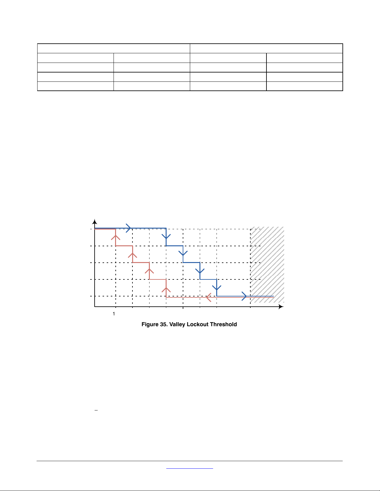
When an “n” valley is asserted by the valley selection
circuitry, the controller locks in this valley until the FB
voltage decreases to the lower threshold (“n+1” valley
activates) or increases to the “n valley threshold” + 600 mV
(“n−1” valley activates). The regulation loop adjusts the
, when P
, when P
nd
2
VLO mode
rd
3
is æ
out
is
out
nd
2
VLO mode
æ
st
1
st
1
peak current to deliver the necessary output power at the
valley operating point. Each valley selection comparator
features a 600−mV hysteresis that helps stabilize operation
despite the FB voltage swing produced by the regulation
loop.
www.onsemi.com
20
Page 21
NCP1362
Table 5. VALLEY FB THRESHOLD ON CONSTANT VOLTAGE REGULATION
FB Falling FB Rising
1st to 2nd Valley 2.5 V FF Mode to 4
2nd to 3rd Valley 2.3 V 4th to 3rd Valley 2.7 V
3rd to 4th Valley 2.1 V 3rd to 2nd Valley 2.9 V
4th to FF Mode 1.9 V 2nd to 1st Valley 3.1 V
th
2.5 V
Frequency Foldback (FF)
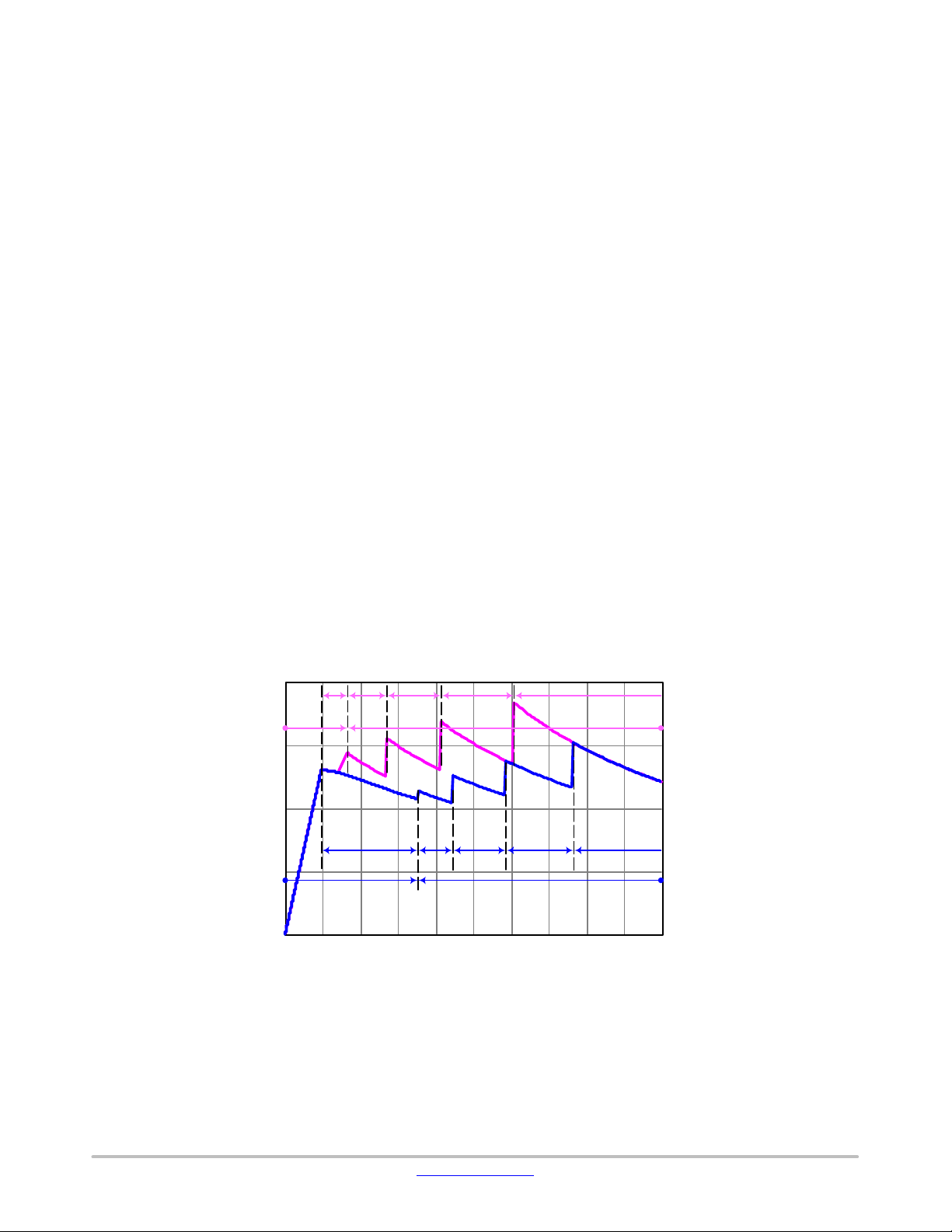
As the output current decreases (FB voltage decreases),
the valleys are incremented from 1 to 4. In case the fourth
valley is reached, the FB voltage further decreases below
1.9 V and the controller enters the frequency foldback mode
(FF). The current setpoint being internally forced to remain
above V
CS(VCO)
(setpoint corresponding to V
Comp
), the
controller regulates the power delivery by modulating the
switching frequency. When an output current increase
causes FB to exceed the 2.5−V FF upper threshold (600−mV
hysteresis), the circuit recovers VLO operation.
In frequency foldback mode, the system reduces the
switching frequency by adding some dead−time after the 4
valley is detected. However, in order to keep the high
Operating
Mode
VCO
th
Valley
4
rd
Valley
3
nd
2
Valley
Pout decreasing
1st Valley
efficiency benefit inherent to the QR operation, the
controller turns on again with the next valley after the dead
time has ended. As a result, the controller will still run in
valley switching mode even when the FF is enabled. This
dead−time increases when the FB voltage decays. There is
no discontinuity when the system transitions from VLO to
FF and the frequency smoothly reduces as FB goes below
1.9 V.
dead−time when V
(1.9 V typ.). At this moment, it can linearly go down to the
th
minimal frequency limit. The generated dead−time is 650 ns
when V
Pout Increasing
The dead−time is selected to generate a 1.15−ms
is decreasing and crossing V
Comp
is increasing and crossing V
Comp
Max Peak
Current
Clamped to
V
= V
CS
HVCOI
ILIM
HVCOD
(2.5 V typ.).
1.9 2.1 2.3 2.5 2.7 2.9 3.1
Figure 35. Valley Lockout Threshold
Stand−by Mode
An high frozen peak current is necessary to have good
efficiency at 10% of the load. On the other hand, the standby
performance will not be optimized. Indeed, in no load
condition, the switching frequency has to be high enough to
have a good transient response and then keep the output
voltage within the limits. If we set a minimum switching
frequency, the only parameter that can be adjusted to deliver
less power is the primary peak current as shown in Eq. 16.
I
p,pk
2
fSW h
(eq. 16)
www.onsemi.com
1
P
+
out
2
V
4.3 V
Comp
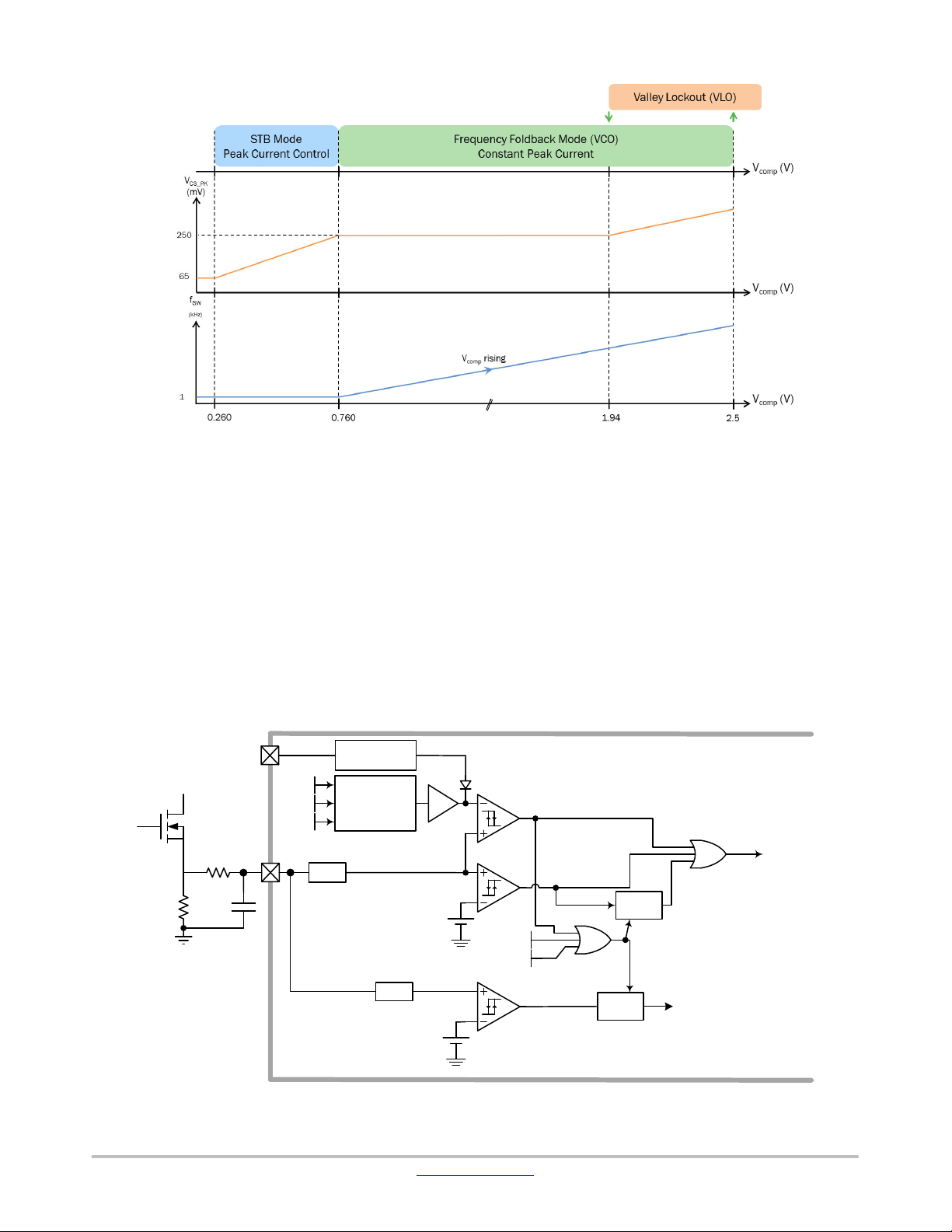
The NCP1362 implements a peak control mode when the
load is closed to 0. From frozen peak current in FF mode
(250 mV here), the maximum voltage threshold on CS pin
is reduced to 65 mV when the Comp voltage crossed
0.260 V. If the 65−mV threshold is reached in 200 ns for
instance due to small primary inductance, the minimum ON
time will be defined by the 320−ns leading edge blanking
duration and the propagation delay (50 ns) so 370 ns
typically.
21
Page 22
NCP1362
Figure 36. Frequency Foldback and Standby Mode Behavior with 1−kHz Minimum Frequency Clamp,
V
CS(VCO)
= 250 mV and V
CS(STB)
= 65 mV
Current Setpoint
As explained in this operating description, the current
setpoint is affected by several functions. Figure 37
summarizes these interactions. As shown by this figure, the
current setpoint is the output of the control law divided by
K
(4 typ.). This current setpoint is clamped by the
comp
soft−start slope as long as the peak current requested by the
FB_CV or FB_CC level are higher. The softstart clamp is
starting from the frozen peak current (V
CS(VCO)
) to V
ILIM
(0.8 V typ.) within 4 ms (tss).
However, this internal FB value is also limited by the
following functions:
LEB1
Peak Current
Control
Control Law
For
Primary Peak
Current Control
LEB2
1/K
comp
V
ILIM
Comp
SoftStart
FB_CV
FB_CC
CS
R
CS
C
R
sense
CS
• A minimum setpoint is forced that equals V
(250 mV, typ.) when 0.760 V < V
comp
CS(VCO)
< 1.9 V
• A second minimum setpoint is forced that equals
V
CS(STB)
(65 mV, typ.) when V
comp
< 0.260 V
• The peak current is linearly reduced between this two
previous frozen peak current (V
CS(VCO)
& V
CS(STB)
• In addition, a second OCP comparator ensures that in
any case the current setpoint is limited to V
ensures the MOSFET current setpoint remains limited
in a fault condition.
ILIM
FB Reset
Max_Ipk reset
Count
4 clk
Counter
OCP
Timer
Reset Timer
Reset
Counter
OCP
SCP
PWM Comp
OCP
Comp
POReset
DbleHiccup
Short Circuit
Comp
to V
ILIM
PWM
Latch
Reset
)
. This
V
CS(Stop )
Figure 37. Current Setpoint
www.onsemi.com
22
Page 23
NCP1362
A 2nd Over−Current Comparator for Abnormal
Overcurrent Fault Detection
A severe fault like a winding short−circuit can cause the
switch current to increase very rapidly during the on−time.
The current sense signal significantly exceeds V
ILIM
. But,
because the current sense signal is blanked by the LEB
circuit during the switch turn on, the power switch current
can abnormally increase, possibly causing system damages.
The NCP1362 protects against this dangerous mode by
adding an additional comparator for abnormal overcurrent
fault detection or short−circuit condition. The current sense
signal is blanked with a shorter LEB duration, t
LEB2
typically 120 ns, before applying it to the short−circuit
comparator. The voltage threshold of this extra comparator,
V
, is typically 1.2 V, set 50% higher than V
CS(stop)
ILIM
. This
is to avoid interference with normal operation. Four
V
DD
V
Jitter
To CS
Comparator
CS
R
consecutive abnormal overcurrent faults cause the
controller to enter in auto−recovery mode. The count to 4
provides noise immunity during surge testing. The counter
is reset each time a DRV pulse occurs without activating the
fault overcurrent comparator or after double hiccup
sequence or if the power supply is unplugged with a new
startup sequence after the initial power on reset.
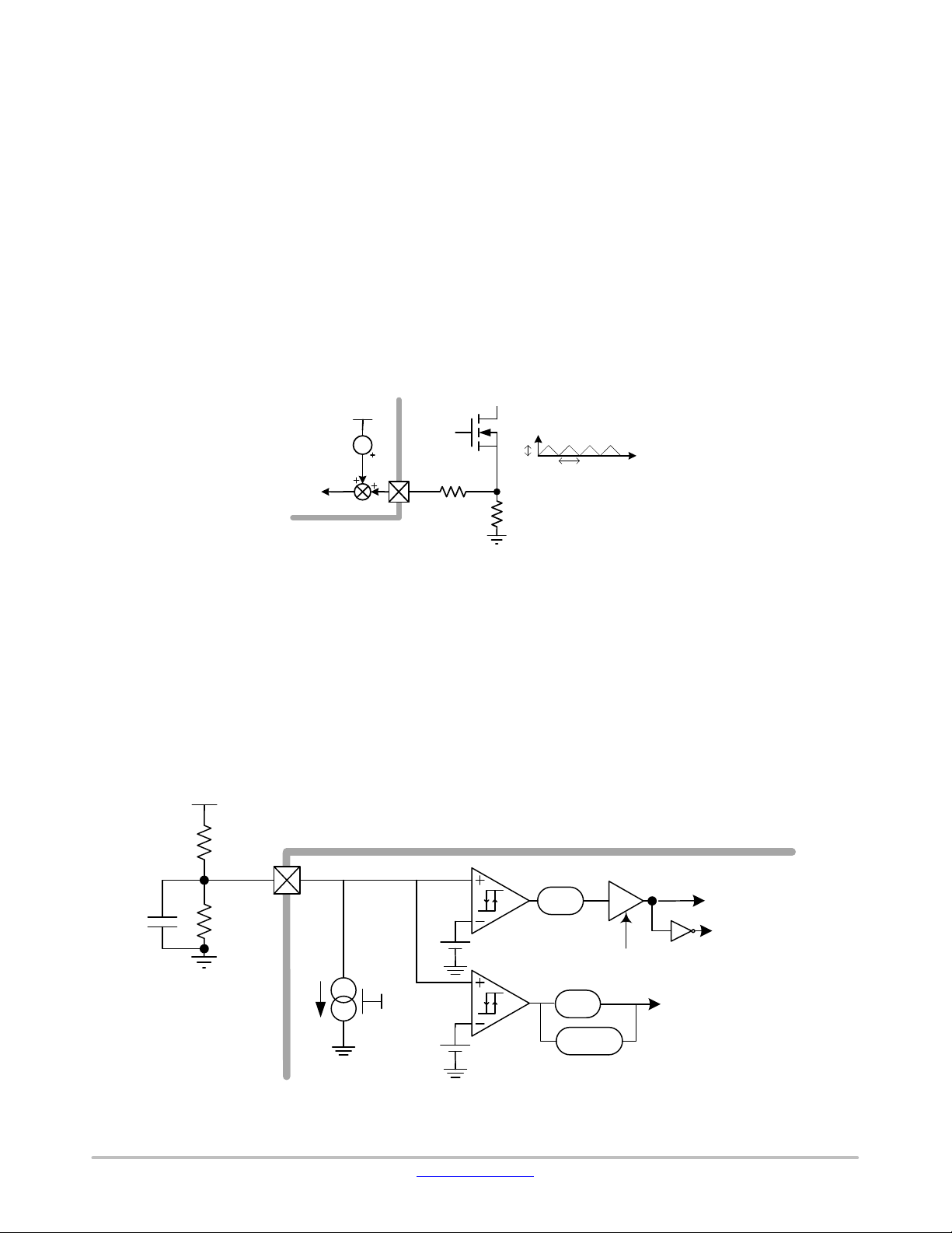
Jittering Capability
In order to help meet the EMI requirements, the NCP1362
features the jittering capability to average the spectrum rays
over the frequency range. The function consists of adding a
,
voltage ripple to the peak current information in order to
change the operation frequency. The peak−to−peak
amplitude of the ripple waveform is 60 mV at 1.5 kHz.
V
CS
Time
LFF
R
V
Sense
jitter
F
jitter
Figure 38. Frequency Jittering
Fault Mode and Protection
• CS Pin: at each startup, a 60−mA (I
) current source
CS
pulls up the CS pin to disable the controller if the pin is
left open or grounded. Then the controller enters in
a double hiccup mode.
• V
/ZCD Pin: after sending the first drive pulse the
S
controller checks the correct wiring of V
/ZCD pin:
S
after the ZCD blanking time, if there is an open or short
conditions, the controller enters in double hiccup mode.
V
bulk
upper
lower
BO/LFF
I
BO
I
BO_en
R
C
BO
R
Brown−out Function
The Brown−out circuitry offers a way to protect the
application from operation under too low input voltage. The
controller allows the output pulses, only if the input voltage
is above V
level. An extra comparator detects if the BO
BO(on)
pin is grounded for disabling the BO feature. The internal
circuitry, depicted by Figure 39, offers a way to observe the
bulk voltage.
Sample
& Hold
BO_EN
BO_DIS
Start−up
BO_OK
V
BO(EN)
V
BO(ON)
1 ms
Filter
50 ms
Filter
1 ms Filter
STB mode
Figure 39. Internal Brown−out Configuration
www.onsemi.com
23
Page 24
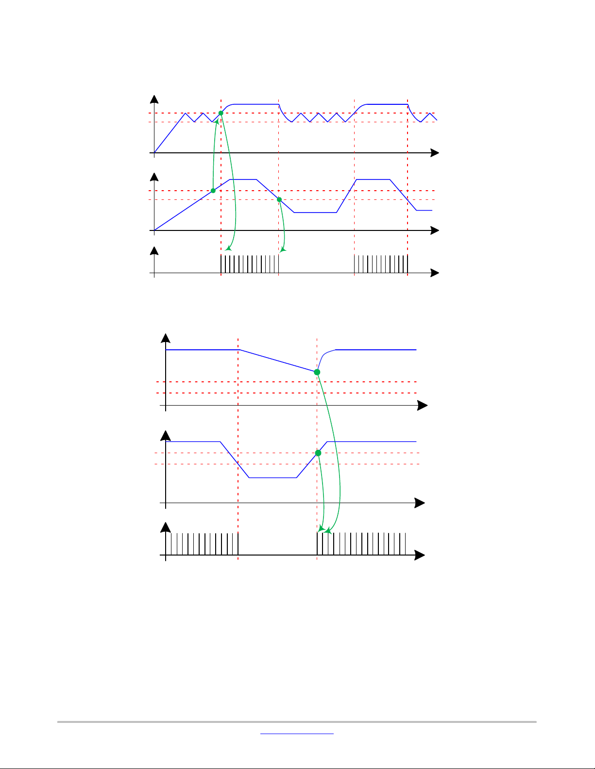
The following figures illustrate the behavior of the
Brown−out pin:
V
CC
V
CC(on)
V
CC(off)
V
BO
V
BO(on)
V
BO(off)
DRV
NCP1362
Time
Time
Time
V
CC(on)
V
CC(off)
V
BO(on)
V
BO(off)
Figure 40. Brown−out Input Functionality − VCC < V
V
CC
V
BO
DRV
CC(on)
Time
Time
Time
Figure 41. Brown−out Input Functionality − VCC > V
www.onsemi.com
24
CC(on)
Page 25
NCP1362
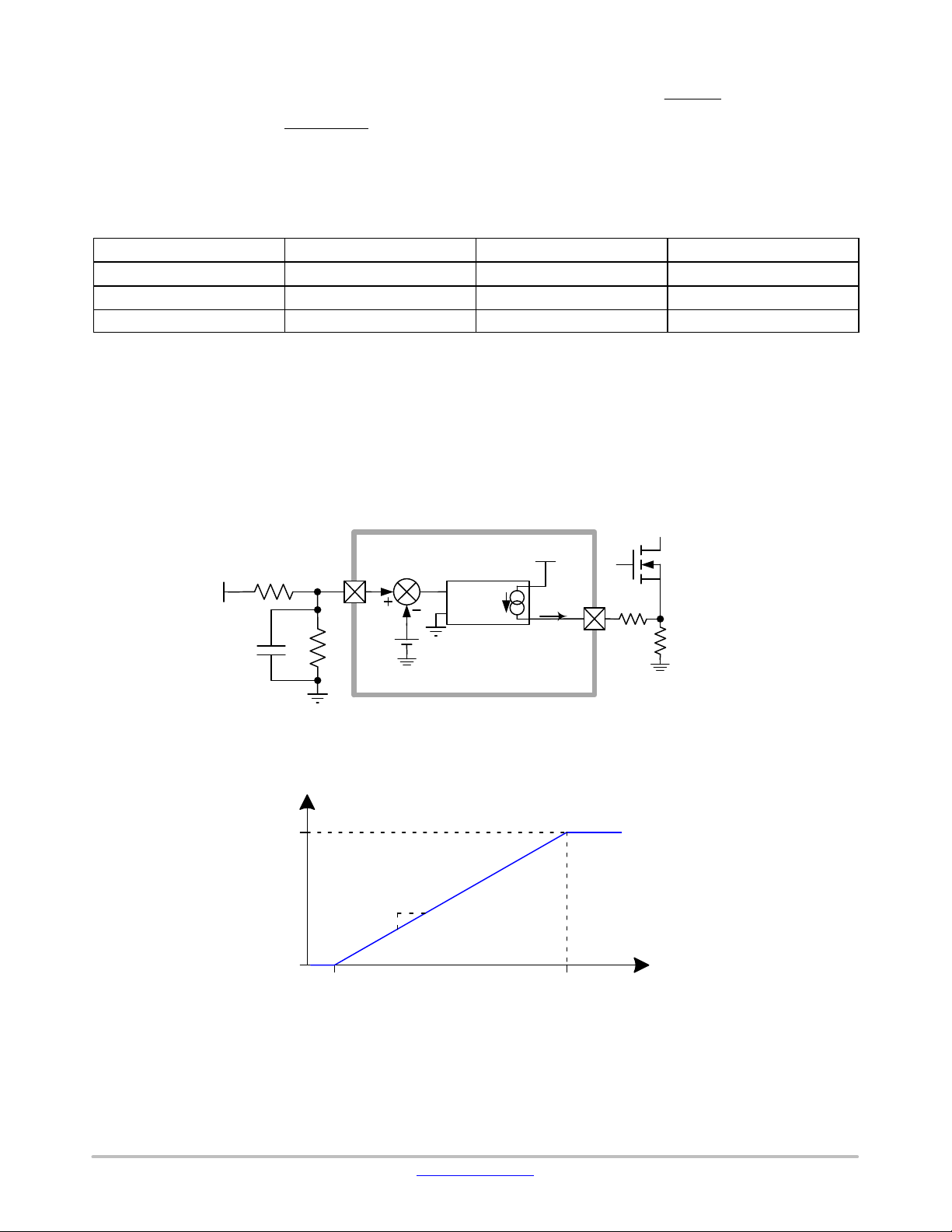
Calculation of the resistors divider:
V
R
lower
+ R
upper
BO(on)
V
* V
bulk
If the power supply must start pulsing at V
= 113 V) with a selected R
(V
bulk
upper
= 10 MW:
BO(on)
(eq. 17)
= 80 V rms
in
Table 6. EXAMPLE OF BROWN−OUT LEVELS WITH R
Parameters BO Pin Level (V) Bulk Level (V) Vin Level (V rms)
V
BO(en)
V
BO(on)
V
BO(off)
0.1 14.0 10
0.8 112.7 79.7
0.7 98.6 69.7
These resistances have to be adjusted after measurements
according to the bulk capacitor ripple and also the capacitor
connected on the BO pin.
There is the possibility for the customer to disable the BO
protection if this function is not needed. To implement this
feature, the BO pin voltage is checked when V
V
after the V
threshold. If the BO voltage is still below V
CC(on)
, the BO function is disabled.
CC(on)
crosses
CC
BO(EN)
R
lower
+ 10 M
0.8
113 * 0.8
+ 71.2 kW
With a selected 71.5−kW normalized ±1% resistor for
R
, it is now possible to calculate all the bulk levels
lower
versus the internal voltage references of the BO pin.
= 71.5 kW & R
lower
Line Feed Forward
upper
= 10 MW
Sensing input line voltage via BO pin allows to generate
a current to CS pin directly proportional to the input line
level in order to compensate the over current on CS pin due
to the propagation delay. The resistor in series with the CS
pin adjusts the compensation level.
(eq. 18)
V
DD
Rupper
BO/LFF
V
bulk
C
BO
Rlower
+
V
k
*V
LFF
−
V
BO(on)
I
LFF
CS
R
LFF
R
Sense
Figure 42. Internal Line Feed Forward Configuration
I
LFF
52 mA
K
= 20 mA/V
LFF
0 mA
V
BO(on)
3.4 V
Figure 43. Transfer Function of the Line Feed Forward
www.onsemi.com
25
Page 26
NCP1362
Calculation of the resistor (R
) for compensating the
LFF
overpower.
Let’s assume the power supply needs to have
a compensation of 45 mV (V
) at 265 V rms (Vin).
LFF
First, it is needed to calculate what is the BO level
corresponding to the line voltage (here 265 V rms) of the
desired compensation level:
V
BO_LFF
+ V
bulk
R
lower
lower
) R
upper
(eq. 19)
R
Then, the resistor value to be inserted between the CS
resistor and CS pin could be calculated, as illustrated here
after:
V
R
LFF
max
1.9 V
1.6 V
ǒV
LFF
BO_LFF
* V
BO(on)
+
K
LFF
Ǔ
Decreases
(eq. 20)
V
Comp
Numerical application yields:
V
BO_LFF
R
+ 265 2Ǹ
+
LFF
mA
(2.66 V * 0.8 V
20
V
71.5 k
71.5 k ) 10 M
45 mV
+ 2.66 V
+ 1.2 kW
)
(eq. 21)
(eq. 22)
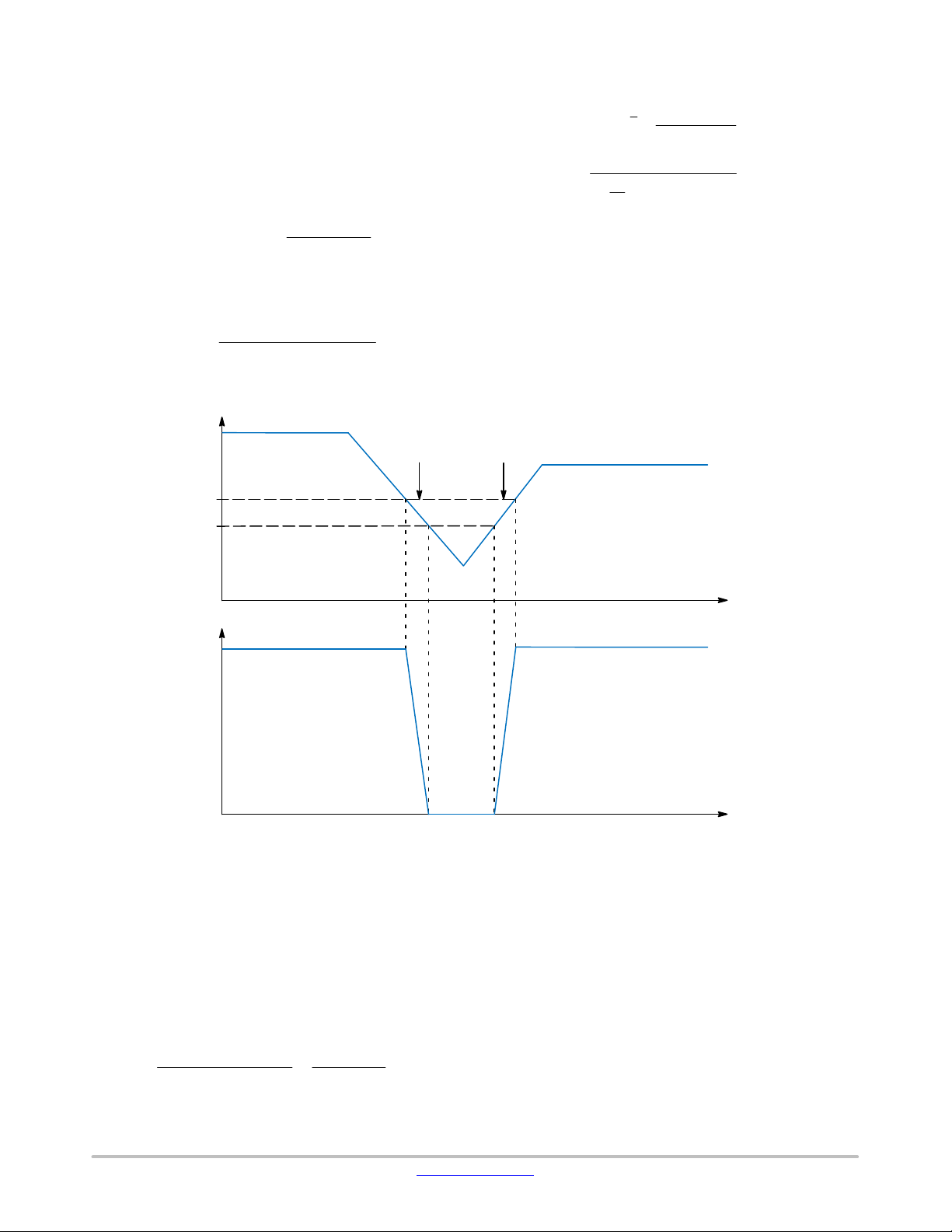
The offset voltage can affect the standby power
performance by reducing the peak current setpoint in
light−load conditions. For this reason, it is desirable to
cancel its action as soon as the VCO mode occurs. A typical
curve variation is shown in Figure 44. At low power, below
the VCO mode starting point, the LFF current is linearly
absorbed and no offset is created through the CS pin when
the Comp pin voltage is below 1.6 V. When feedback
increases again and reaches the 1.6−V threshold, OPP starts
to build up and reaches its full value at 1.9 V.
V
Comp
Increases
100
0 t
Figure 44. The LFF Current is Applied when the Comp Voltage Exceeds 1.6 V. It is 0 below it
Fault Input
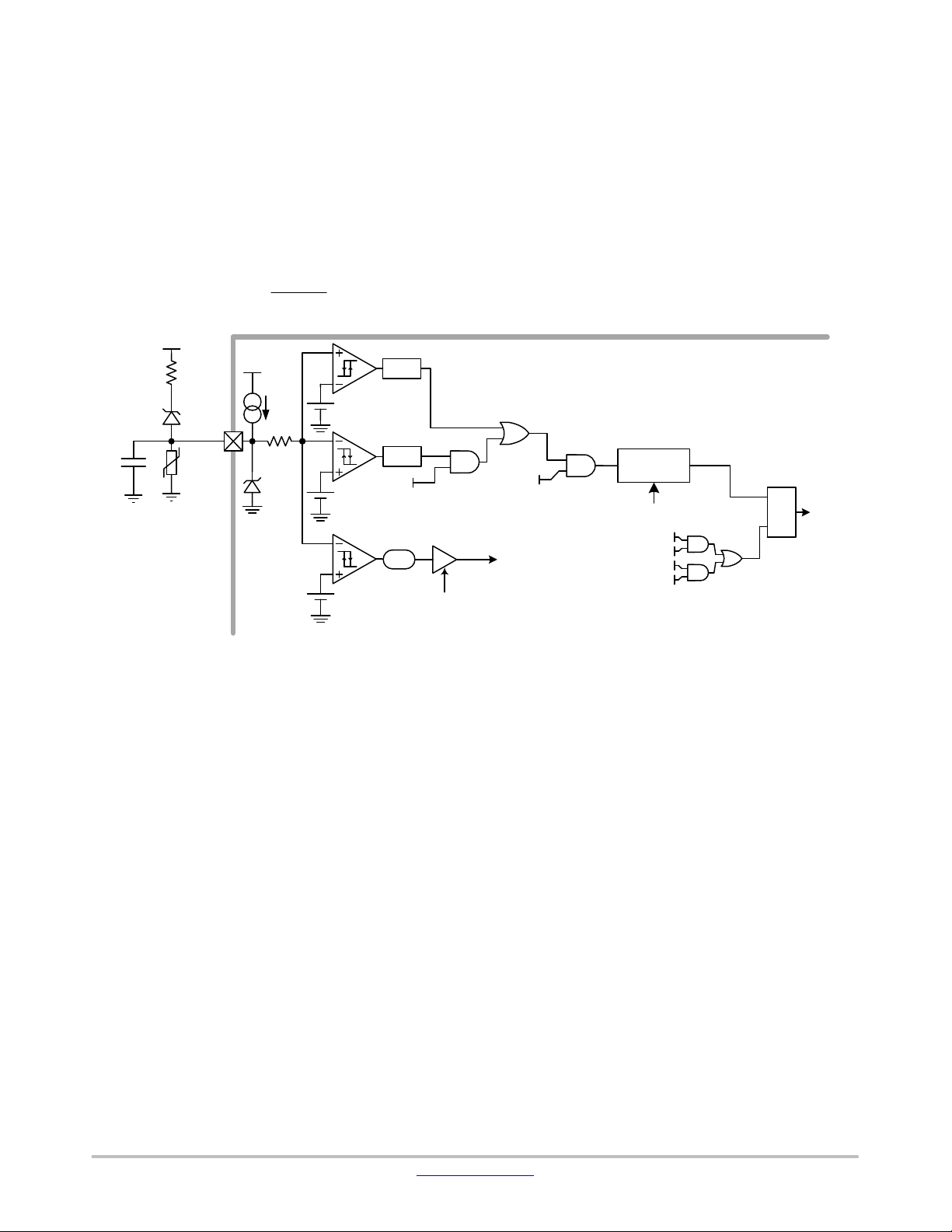
The NCP1362 includes a dedicated fault input accessible
via the Fault pin. Figure 45 shows the architecture of the
Fault input. The controller can be latched by pulling up the
pin above the upper fault threshold, V
Fault(OVP)
, typically
3.0 V. An active clamp prevents the Fault pin voltage from
reaching the V
Fault(OVP)
if the pin is open. To reach the upper
threshold, the external pull−up current has to be higher than
the pull−down capability of the clamp.
V
Fault(OVP)
i.e. approximately 1.2 mA.
* V
R
Fault(clamp)
Fault(clamp)
3V* 1.35 V
+
1.35 kW
,
(eq. 23)
t
This function is typically used to detect a VCC or auxiliary
winding overvoltage by means of a Zener diode generally in
series with a small resistor (see Figure 45).
Neglecting the resistor voltage drop, the OVP threshold is
then:
V
AUX(OVP)
+ VZ) V
Fault(OVP)
(eq. 24)
where VZ is the Zener diode voltage.
The controller can also be latched off if the Fault pin
voltage, V
V
Fault(OTP)
, is pulled below the lower fault threshold,
Fault
, typically 0.4 V. This capability is normally used
for detecting an overtemperature fault by means of an NTC
www.onsemi.com
26
Page 27
NCP1362
thermistor. A pull up current source I
Fault(OTP)
, (typically
45 mA) generates a voltage drop across the thermistor. The
resistance of the NTC thermistor decreases at higher
temperatures resulting in a lower voltage across the
thermistor. The controller detects a fault once the thermistor
voltage drops below V
Fault(OTP)
.
The circuit detects an overtemperature situation when:
R
NTC
I
Fault(OVP)
+ V
Fault(OVP)
(eq. 25)
Hence, the OTP protection trips when
V
V
+
DD
R
Fault(OVP)
I
Fault(OTP)
I
fault(OTP)
fault(clamp)
V
fault(clamp)
V
V
Fault(OTP)
V
Fault(EN)
Fault(OVP)
R
NTC
Vaux
V
Z
Fault
NTC
Blanking
2 ms
Blanking
SS
1 ms
Filter
(eq. 26)
2 ms
end
Sample
& Hold
Start−up
that is 8.9 kW typically.
The controller bias current is reduced during power up by
disabling most of the circuit blocks including I
This current source is enabled once V
CC
Fault(OTP)
reaches V
CC(on)
A bypass capacitor is usually connected between the Fault
and GND pins. It will take some time for V
steady state value once I
Fault(OTP)
is enabled. Therefore, the
to reach its
Fault
lower fault comparator (i.e. overtemperature detection) is
ignored during soft−start.
Clock
Fault pin
disabled
Up Counter
Reset
OVP/OTP gone
BO_DIS
V
CC(Reset)
BO_EN
BO_NOK
Fault
4
S
Latch
Q
R
.
.
Figure 45. Fault Detection Schematic
As a matter of fact, the controller operates normally while
the Fault pin voltage is maintained within the upper and
lower fault thresholds. Upper and lower fault detector have
blanking delays to prevent noise from triggering them. Both
OVP and OTP comparator output are validated only if its
high−state duration lasts a minimum of 2 ms. Below this
value, the event is ignored. Then, a counter ensures that
OVP/OTP events occurred for 4 successive drive clock
pulses before actually latching the part.
When the part is latched−off, the drive is immediately
turned off and V
goes in endless hiccup mode. The power
CC
supply needs to be un−plugged to reset the part as a result of
a BO_NOK (BO fault condition) if Brown−Out feature is
enabled otherwise V
CC(Reset)
.
There is the possibility for the customer to disable the fault
pin protection if this function is not needed or to reduce the
IC consumption in stand−by mode. To implement this
feature, the fault pin voltage is checked when V
V
after the V
threshold. If the voltage is still below V
CC(on)
, the fault pin is disabled.
CC(on)
crosses
CC
Fault(EN)
Thermal Shutdown
An internal thermal shutdown circuit monitors the
junction temperature of controller die of the IC. The
controller is disabled if its junction temperature exceeds the
thermal shutdown threshold (T
). A continuous V
SHDN
CC
hiccup is initiated after a thermal shutdown fault is detected.
The controller restarts at the next V
temperature drops below T
shutdown hysteresis (T
also cleared if V
SHDN(off)
drops below V
CC
sequences commences at the next V
reduced by the thermal
SHDN
). The thermal shutdown is
CC(reset)
CC(on)
once the IC
CC(on)
. A new power up
once all the faults
are removed.
www.onsemi.com
27
Page 28

NCP1362
Table 7. ORDERING TABLE OPTION
OPN #
NCP1362_ _
NCP1362AADR2G x x x
NCP1362ABDR2G x x x
Table 8. ORDERING INFORMATION
Device Device Marking Package Shipping
NCP1362AADR2G P1362AA
NCP1362ABDR2G P1362AB
†For information on tape and reel specifications, including part orientation and tape sizes, please refer to our Tape and Reel Packaging
Specifications Brochure, BRD8011/D.
Minimum Switching
Frequency in VCO Mode (kHz)
0.2 1 No 80 110 140 Enable Disable
Maximum Switching Frequency (kHz) Jittering Frequency
SOIC−8
(Pb−Free)
2500 / Tape & Reel
†
www.onsemi.com
28
Page 29
0.20 C
NOTES 4&5
D
85
E E1
14
D
B
NOTE 6
TOP VIEW
A
A1
SIDE VIEW
NOTE 8
SIDE VIEW
D
NOTE 6
A
e
0.10 C D
2X
0.10 C
NOTES 4&5
b8X
0.25 A-B
NOTES 3&7
A2
SEATING
C
PLANE
M
0.10 C
NCP1362
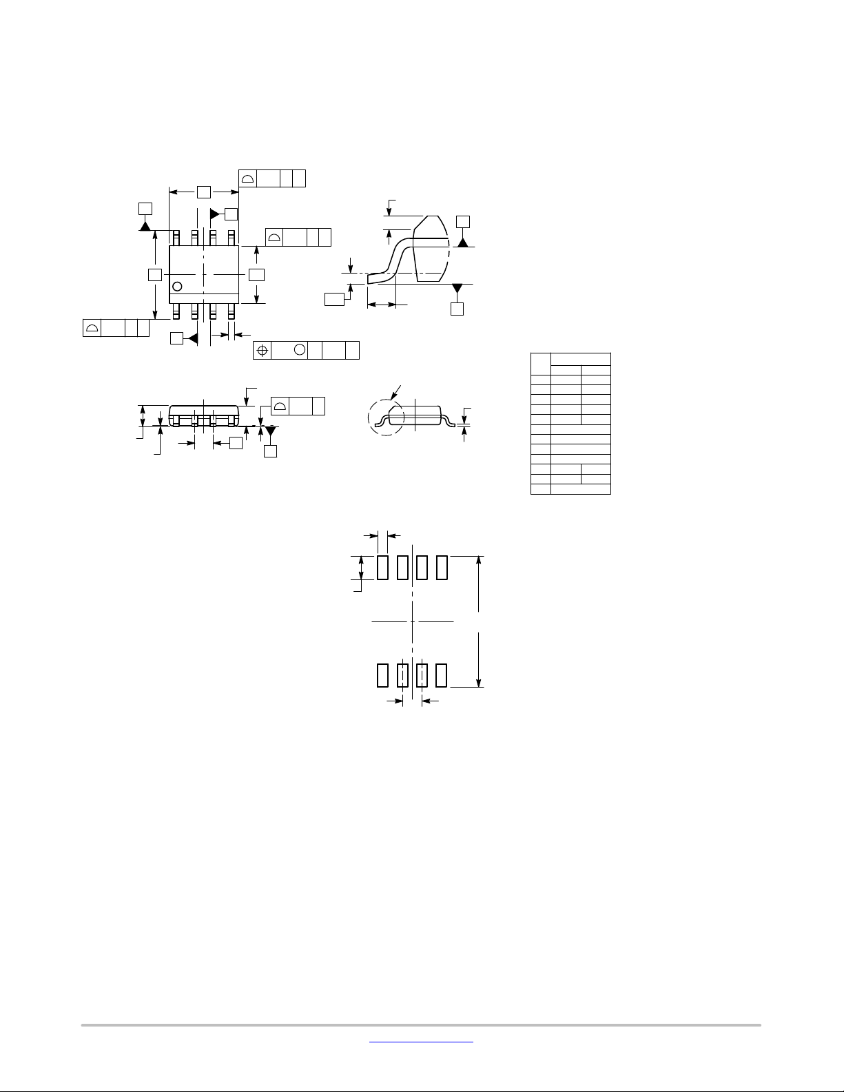
PACKAGE DIMENSIONS
SOIC−8
CASE 751AZ
ISSUE B
45 CHAMFER5
h
D
L2
D
C
RECOMMENDED
SOLDERING FOOTPRINT*
L
DETAIL A
DETAIL A
END VIEW
8X
0.76
H
C
NOTE 7
SEATING
PLANE
c
NOTES:
1. DIMENSIONING AND TOLERANCING PER ASME Y14.5M, 1994.
2. CONTROLLING DIMENSION: MILLIMETERS.
3. DIMENSION b DOES NOT INCLUDE DAMBAR PROTRUSION.
ALLOWABLE PROTRUSION SHALL BE 0.004 mm IN EXCESS OF
MAXIMUM MATERIAL CONDITION.
4. DIMENSION D DOES NOT INCLUDE MOLD FLASH, PROTRUSIONS
OR GATE BURRS. MOLD FLASH, PROTRUSIONS OR GATE BURRS
SHALL NOT EXCEED 0.006 mm PER SIDE. DIMENSION E1 DOES
NOT INCLUDE INTERLEAD FLASH OR PROTRUSION. INTERLEAD
FLASH OR PROTRUSION SHALL NOT EXCEED 0.010 mm PER SIDE.
5. THE PACKAGE TOP MAY BE SMALLER THAN THE PACKAGE BOT
TOM. DIMENSIONS D AND E1 ARE DETERMINED AT THE OUTER
MOST EXTREMES OF THE PLASTIC BODY AT DATUM H.
6. DIMENSIONS A AND B ARE TO BE DETERMINED AT DATUM H.
7. DIMENSIONS b AND c APPLY TO THE FLAT SECTION OF THE LEAD
BETWEEN 0.10 TO 0.25 FROM THE LEAD TIP.
8. A1 IS DEFINED AS THE VERTICAL DISTANCE FROM THE SEATING
PLANE TO THE LOWEST POINT ON THE PACKAGE BODY.
MILLIMETERS
DIM MIN MAX
A --- 1.75
A1 0.10 0.25
A2 1.25 ---
b 0.31 0.51
c 0.10 0.25
D 4.90 BSC
E 6.00 BSC
E1 3.90 BSC
e 1.27 BSC
h 0.25 0.41
L 0.40 1.27
0.25 BSC
L2
8X
1.52
7.00
1
1.27
PITCH
DIMENSIONS: MILLIMETERS
*For additional information on our Pb−Free strategy and soldering
details, please download the ON Semiconductor Soldering and
Mounting Techniques Reference Manual, SOLDERRM/D.
www.onsemi.com
29
Page 30

ON Semiconductor and are trademarks of Semiconductor Components Industries, LLC dba ON Semiconductor or its subsidiaries in the United States and/or other countries.
ON Semiconductor owns the rights to a number of patents, trademarks, copyrights, trade secrets, and other intellectual property. A listing of ON Semiconductor’s product/patent
coverage may be accessed at www.onsemi.com/site/pdf/Patent−Marking.pdf
ON Semiconductor makes no warranty, representation or guarantee regarding the suitability of its products for any particular purpose, nor does ON Semiconductor assume any liability
arising out of the application or use of any product or circuit, and specifically disclaims any and all liability, including without limitation special, consequential or incidental damages.
Buyer is responsible for its products and applications using ON Semiconductor products, including compliance with all laws, regulations and safety requirements or standards,
regardless of any support or applications information provided by ON Semiconductor. “Typical” parameters which may be provided in ON Semiconductor data sheets and/or
specifications can and do vary in different applications and actual performance may vary over time. All operating parameters, including “Typicals” must be validated for each customer
application by customer’s technical experts. ON Semiconductor does not convey any license under its patent rights nor the rights of others. ON Semiconductor products are not
designed, intended, or authorized for use as a critical component in life support systems or any FDA Class 3 medical devices or medical devices with a same or similar classification
in a foreign jurisdiction or any devices intended for implantation in the human body. Should Buyer purchase or use ON Semiconductor products for any such unintended or unauthorized
application, Buyer shall indemnify and hold ON Semiconductor and its officers, employees, subsidiaries, affiliates, and distributors harmless against all claims, costs, damages, and
expenses, and reasonable attorney fees arising out of, directly or indirectly, any claim of personal injury or death associated with such unintended or unauthorized use, even if such
claim alleges that ON Semiconductor was negligent regarding the design or manufacture of the part. ON Semiconductor is an Equal Opportunity/Affirmative Action Employer. This
literature is subject to all applicable copyright laws and is not for resale in any manner.
. ON Semiconductor reserves the right to make changes without further notice to any products herein.
PUBLICATION ORDERING INFORMATION
LITERATURE FULFILLMENT:
Email Requests to: [email protected]
ON Semiconductor Website: www.onsemi.com
TECHNICAL SUPPORT
North American Technical Support:
Voice Mail: 1 800−282−9855 Toll Free USA/Canada
Phone: 011 421 33 790 2910
Europe, Middle East and Africa Technical Support:
Phone: 00421 33 790 2910
For additional information, please contact your local Sales Representative
◊
www.onsemi.com
1
 Loading...