

LDO Regulator, 150 mA,
38V, 1 mA I
, with PG
Q
NCP730
The NCP730 device is based on unique combination of features −
very low quiescent current, fast transient response and high input and
output voltage ranges. The NCP730 is CMOS LDO regulator designed
for up to 38 V input voltage and 150 mA output current. Quiescent
current of only 1 mA makes this device ideal solution for battery−
powered, always−on systems. Several fixed output voltage versions
are available as well as the adjustable version.
The device (version B) implements power good circuit (PG) which
indicates that output voltage is in regulation. This signal could be used
for power sequencing or as a microcontroller reset.
Internal short circuit and over temperature protections saves the
device against overload conditions.
Features
• Operating Input Voltage Range: 2.7 V to 38 V
• Output Voltage: 1.2 V to 24 V
• Capable of Sourcing 200 mA Peak Output Current
• Very Low Quiescent Current: 1 mA typ.
• Low Dropout: 290 mV typ. at 150 mA, 3.3 V Version
• Output Voltage Accuracy ±1%
• Power Good Output (Version B)
• Stable with Small 1 mF Ceramic Capacitors
• Built−in Soft Start Circuit to Suppress Inrush Current
• Over−Current and Thermal Shutdown Protections
• Available in Small TSOP−5 and WDFN6 (2x2) Packages
• These Devices are Pb−Free and are RoHS Compliant
Typical Applications
• Battery Power Tools and Equipment
• Home Automation
• RF Devices
• Metering
• Remote Control Devices
• White Goods
www.onsemi.com
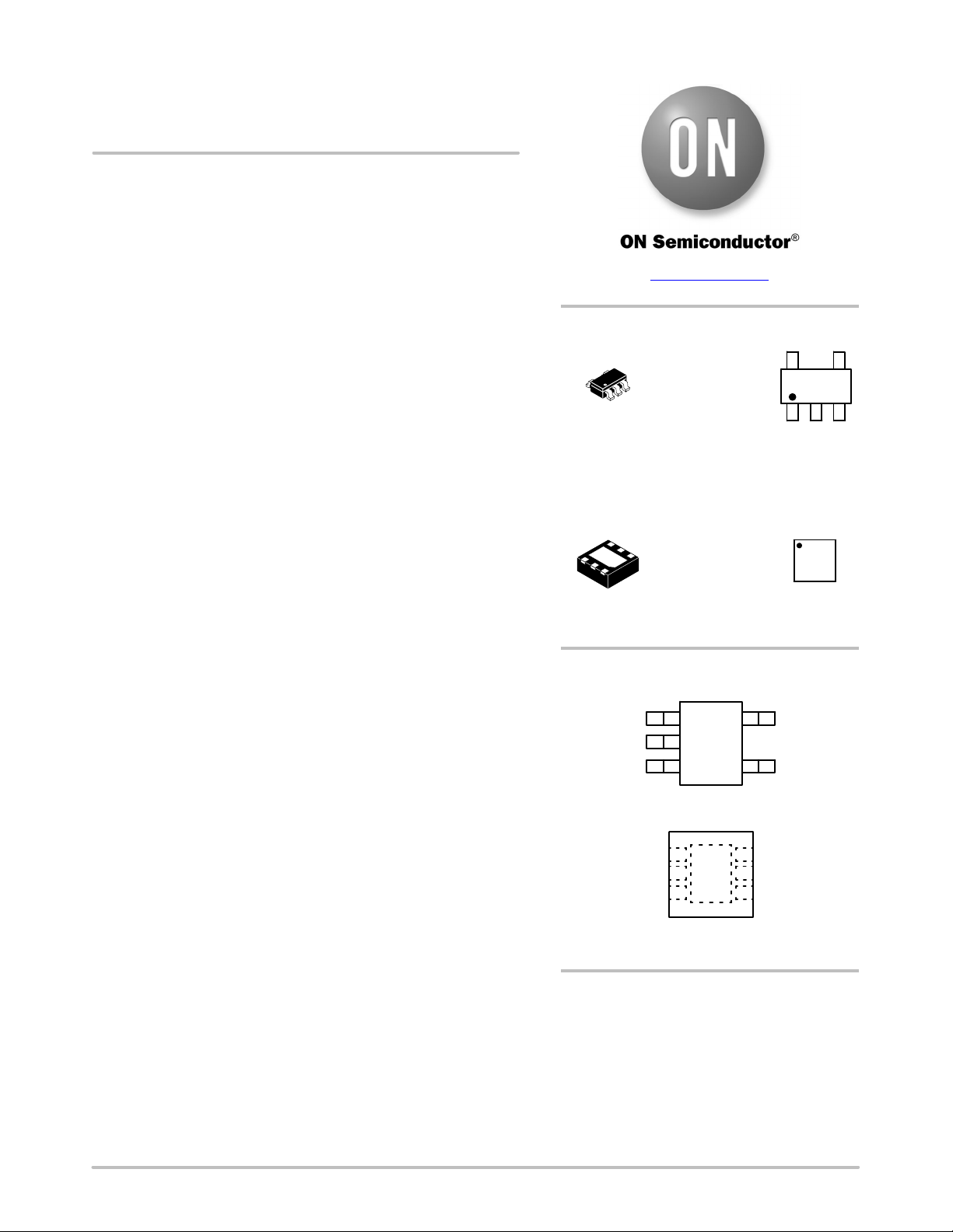
MARKING DIAGRAMS
TSOP−5
5
1
(Note: Microdot may be in either location)
1
GND
SN SUFFIX
CASE 483
XXX = Specific Device Code
A = Assembly Location
Y = Year
W = Work Week
G = Pb−Free Package
WDFN6 (2x2)
MT SUFFIX
CASE 511BR
XX = Specific Device Code
M = Date Code
PIN ASSIGNMENTS
TSOP−5
IN
EN
NC/ADJ 2
1
2
3
CASE 483
WDFN6 (2x2)
OUT 1
EP
GND 3
5
1
5
4
6 IN
5 NC/PG
4 EN
XXXAYWG
G
1
XX M
OUT
NC/ADJ/PG
© Semiconductor Components Industries, LLC, 2018
March, 2021 − Rev. 1
CASE511BR
(Top Views)
ORDERING INFORMATION
See detailed ordering and shipping information on page 29 of
this data sheet.
1 Publication Order Number:
NCP730/D
NCP730
Ǔ
TYPICAL APPLICATION SCHEMATICS
C
1nF
V
OUT=5V
C
1mF
OUT
FF
V
IN=6−38V
C
IN
1mF
OFF
IN
NCP730A 5.0V
TSOP−5 / WDFN−6
ON
EN
GND
OUT
NC
V
OUT=5.0V
C
1mF
OUT
V
IN=6−38V
C
IN
1mF
OFF
IN
NCP730A ADJ
TSOP−5 / WDFN−6
ON
EN
GND
OUT
ADJ
1.2V
R1
2M4
R2
750k
Figure 1. Fixed Output Voltage Application (No PG) Figure 2. Adjustable Output Voltage Application (No PG)
V
IN=6−38V
C
IN
1mF
OFF
IN
NCP730B 5.0V
TSOP−5 / WDFN−6
ON
EN
GND
OUT
NC
PG
R
PG
100k
V
OUT=5.0V
PG
C
1mF
OUT
V
IN=6−38V
C
IN
1mF
OFF
ON
IN
NCP730B ADJ
Only WDFN−6
EN
GND
OUT
ADJ
PG
1.2V
R1
2M4
R2
750k
C
1nF
FF
C
1mF
V
OUT
OUT=5V
R
100k
PG
PG
Figure 3. Fixed Output Voltage Application with PG Figure 4. Adjustable Output Voltage Application with PG
R
V
OUT
+ V
ADJ
@ǒ1 )
1
) I
@ R
1
R
ADJ
2
EN
IN
OUT
UVLO Comparator
UVLO
1.95 V
V
= 300nA
EN−PU
I
CCEN
V−REFERENCE
AND SOFT−START
V
REF
1.2V
EA
Current limit
R
ADJ1
VFB=1.2V
Enable
EN Comparator
0.9 V
THERMAL
SHUTDOWN
PG Comparator
93% of V
Note:
REF
Blue objects are valid for ADJ version
Green objects are valid for FIX version
DEGLITCH
DELAY TMR
R
ADJ2
ADJ
GND
PG
NC
Brown objects are valid for B version (with PG)
Figure 5. Internal Block Diagram
www.onsemi.com
2
NCP730
PIN DESCRIPTION − TSOP−5 package
Pin No. Pin Name Description
1 IN Power supply input pin.
2 GND Ground pin.
3 EN Enable input pin (high − enabled, low − disabled). If this pin is connected to IN pin or if it is left uncon-
4 ADJ/PG/NC ADJ (ADJ device version only):
5 OUT Output pin.
PIN DESCRIPTION − WDFN−6 package
Pin No. Pin Name Description
1 OUT Output pin.
2 NC/ADJ ADJ (ADJ device version only):
3 GND Ground pin.
4 EN Enable input pin (high − enabled, low − disabled). If this pin is connected to IN pin or if it is left
5 NC/PG PG (ADJ/FIX device versions with PG functionality):
6 IN Power supply input pin.
EP EPAD Exposed pad pin. Should be connected to the GND plane.
nected (pull−up resistor is not required) the device is enabled.
• Adjust input pin. Could be connected to the output resistor divider or to the output pin directly.
PG (FIX device versions with PG functionality):
• Power good output pin. High level for power ok, low level for fail. If not used, could be left
unconnected or shorted to GND.
NC (FIX device versions without PG functionality):
• Not internally connected. This pin can be tied to the ground plane to improve thermal dissipation.
• Adjust input pin. Could be connected to the output resistor divider or to the output pin directly.
NC (all FIX device versions):
• Not internally connected. This pin can be tied to the ground plane to improve thermal dissipation.
unconnected (pull−up resistor is not required) the device is enabled.
• Power good output pin. High level for power ok, low level for fail. If not used, could be left
unconnected or shorted to GND.
NC (ADJ/FIX device versions without PG functionality):
• Not internally connected. This pin can be tied to the ground plane to improve thermal dissipation.
www.onsemi.com
3
NCP730
MAXIMUM RATINGS
Rating Symbol Value Unit
VIN Voltage (Note 1)
VOUT Voltage
EN Voltage
ADJ Voltage
PG Voltage
Output Current
PG Current
Maximum Junction Temperature
Storage Temperature
ESD Capability, Human Body Model (Note 2)
ESD Capability, Charged Device Model (Note 2)
Stresses exceeding those listed in the Maximum Ratings table may damage the device. If any of these limits are exceeded, device functionality
should not be assumed, damage may occur and reliability may be affected.
1. Refer to ELECTRICAL CHARACTERISTICS and APPLICATION INFORMATION for Safe Operating Area.
2. This device series incorporates ESD protection and is tested by the following methods:
ESD Human Body Model tested per ANSI/ESDA/JEDEC JS−001, EIA/JESD22−A114
ESD Charged Device Model tested per ANSI/ESDA/JEDEC JS−002, EIA/JESD22−C101
THERMAL CHARACTERISTICS (Note 3)
Characteristic Symbol WDFN6 2x2 TSOP−5 Unit
Thermal Resistance, Junction−to−Air R
Thermal Resistance, Junction−to−Case (top) R
Thermal Resistance, Junction−to−Case (bottom) R
Thermal Resistance, Junction−to−Board (top) R
Thermal Characterization Parameter, Junction−to−Case (top) Psi
Thermal Characterization Parameter, Junction−to−Board [FEM] Psi
3. Measured according to JEDEC board specification (board 1S2P, Cu layer thickness 1 oz, Cu area 650 mm2, no airflow). Detailed description
of the board can be found in JESD51−7.
ELECTRICAL CHARACTERISTICS (V
(effective capacitance – Note 4), T
Parameter
Recommended Input Voltage V
Output Voltage Accuracy
ADJ Reference Voltage ADJ version only V
ADJ Input Current V
Line Regulation VIN = V
Load Regulation I
Quiescent Current (version A) VIN = V
Quiescent Current (version B) VIN = V
Ground Current I
Shutdown Current (Note 9) VEN = 0 V, I
Output Current Limit V
Short Circuit Current V
Dropout Voltage (Note 6) I
Power Supply Ripple Rejection VIN = V
= −40°C to 125°C, ADJ tied to OUT, unless otherwise specified) (Note 5)
J
IN
= V
OUT−NOM
+ 1 V and VIN ≥ 2.7 V, VEN = 1.2 V, I
Test Conditions Symbol Min Ty p Max Unit
TJ = −40°C to +85°C
TJ = −40°C to +125°C −1 − 2
= 1.2 V I
ADJ
OUT−NOM
= 0.1 mA to 150 mA
OUT
OUT−NOM
OUT−NOM
= 150 mA I
OUT
= V
OUT
= 0 V I
OUT
= 150 mA V
OUT
OUT−NOM
I
= 10 mA
OUT
+ 1 V to 38 V and VIN ≥ 2.7 V
+ 1 V to 38 V, I
+ 1 V to 38 V, I
= 0 mA, VIN = 38 V I
OUT
OUT−NOM
+ 2 V
V
IN
V
V
V
FB/ADJ
V
I
T
J(MAX)
T
ESD
ESD
OUT
EN
PG
OUT
I
PG
STG
HBM
CDM
−0.3 to [(VIN + 0.3) or 40 V; whichever is lower]
thJA
thJCt
thJCb
thJBt
JCt
JB
= 0 mA
OUT
= 0 mA − 1.8 3.0
OUT
− 100 mV I
10 Hz
−0.3 to 40 V
−0.3 to (VIN + 0.3) V
−0.3 to 5.5 V
−0.3 to (VIN + 0.3) V
Internally limited mA
3 mA
150 °C
−55 to 150 °C
2000 V
1000 V
61 142 °C/W
200 80 °C/W
14 N/A °C/W
46 110 °C/W
3 21 °C/W
46 113 °C/W
= 1 mA, CIN = C
OUT
2.7 − 38 V
−1 − 1
− 1.2 − V
−0.1 0.01 0.1
− − 0.2 %V
− − 0.4 %V
− 1.3 2.5 mA
− 325 450
− 0.35 1.5
200 280 450 mA
200 280 450 mA
− 290 480 mV
− 80 −
V
DV
DV
GND
SHDN
OLIM
OSC
PSRR
IN
OUT
ADJ
ADJ
O(DVI)
O(DIO)
I
Q
DO
10 kHz − 70 −
OUT
V
= 1.0 mF
%
mA
OUT
OUT
mA
mA
dB
www.onsemi.com
4
NCP730
ELECTRICAL CHARACTERISTICS (V
(effective capacitance – Note 4), T
= −40°C to 125°C, ADJ tied to OUT, unless otherwise specified) (Note 5) (continued)
J
IN
= V
OUT−NOM
+ 1 V and VIN ≥ 2.7 V, VEN = 1.2 V, I
= 1 mA, CIN = C
OUT
OUT
= 1.0 mF
Parameter UnitMaxTypMinSymbolTest Conditions
Power Supply Ripple Rejection VIN = V
I
OUT
OUT−NOM
= 10 mA
Output Voltage Noise f = 10 Hz to 100 kHz
+ 2 V
100 kHz
PSRR
− 42 −
1 MHz − 48 −
FIX−3.3 V
V
N
− 195 − mV
dB
RMS
FIX−5.0 V − 240 −
FIX−15.0 V − 460 −
ADJ set to 5.0 V
C
= 100 pF
FF
ADJ set to 5.0 V
C
= 10 nF
FF
EN Threshold VEN rising V
EN Hysteresis VEN falling V
EN Internal Pull−up Current VEN = 1 V, VIN = 5.5 V I
EN−PU
EN Input Leakage Current VEN = 30 V, VIN = 30 V I
Start−up time (Note 7)
V
OUT−NOM
V
OUT−NOM
≤ 3.3 V
> 3.3 V 300 600 1000
t
Internal UVLO Threshold Ramp VIN up until output is turned on V
Internal UVLO Hysteresis Ramp VIN down until output is turned off V
PG Threshold (Note 8) V
PG Hysteresis (Note 8) V
PG Deglitch Time (Note 8) t
PG Delay Time (Note 8) t
falling V
OUT
rising V
OUT
PG−DG
PG−DLY
PG Output Low Level Voltage (Note 8) IPG = 1 mA V
PG Output Leakage Current (Note 8) VPG = 30 V I
Thermal Shutdown Temperature Temperature rising from TJ = +25°C T
Thermal Shutdown Hysteresis Temperature falling from T
SD
EN−TH
EN−HY
EN−LK
START
IUL−TH
IUL−HY
PG−TH
PG−HY
PG−OL
PG−LK
SD
T
SDH
− 132 −
− 82 −
0.7 0.9 1.05 V
0.01 0.1 0.2 V
0.01 0.3 1
−1 0.05 1
100 250 500 ms
1.6 1.95 2.6 V
0.05 0.2 0.3 V
90 93 96 %
0.1 2 4 %
75 160 270
120 320 600
− 0.2 0.4 V
− 0.01 1
− 165 − °C
− 20 − °C
mA
mA
ms
ms
mA
Product parametric performance is indicated in the Electrical Characteristics for the listed test conditions, unless otherwise noted. Product
performance may not be indicated by the Electrical Characteristics if operated under different conditions.
4. Effective capacitance, including the effect of DC bias, tolerance and temperature. See the Application Information section for more
information.
5. Performance guaranteed over the indicated operating temperature range by design and/or characterization. Production tested at T
Low duty cycle pulse techniques are used during the testing to maintain the junction temperature as close to ambient as possible.
= 25°C.
A
6. Dropout measured when the output voltage falls 100 mV below the nominal output voltage. Limits are valid for all voltage versions.
7. Startup time is the time from EN assertion to point when output voltage is equal to 95% of V
8. Applicable only to version B (device option with power good output). PG threshold and PG hysteresis are expressed in percentage of nominal
OUT−NOM
.
output voltage.
9. Shutdown current includes EN Internal Pull−up Current.
www.onsemi.com
5
VIN = V
OUT−NOM
2.0%
V
= (V
IN
I
= 1 to 150 mA
OUT
1.5%
1.0%
(V)
OUT
0.5%
0.0%
-0.5%
-1.0%
OUTPUT VOLTAGE, V
-1.5%
+ 1 V and VIN ≥ 2.7 V, VEN = 1.2 V, I
+ 1 V) to 38 V, VIN≥ 2.7 V
OUT-NOM
= 15 V
V
OUT-NOM
V
= 1.2 V
OUT-NOM
NCP730
TYPICAL CHARACTERISTICS
OUT
High limit
V
OUT-NOM
Low limit
= 1 mA, C
= 5 V
= 1.0 mF, ADJ tied to OUT, TJ = 25°C, unless otherwise specified
OUT
-2.0%
-40 -20 0 20 40 60 80 100
JUNCTION TEMPERATURE, TJ(°C)
120
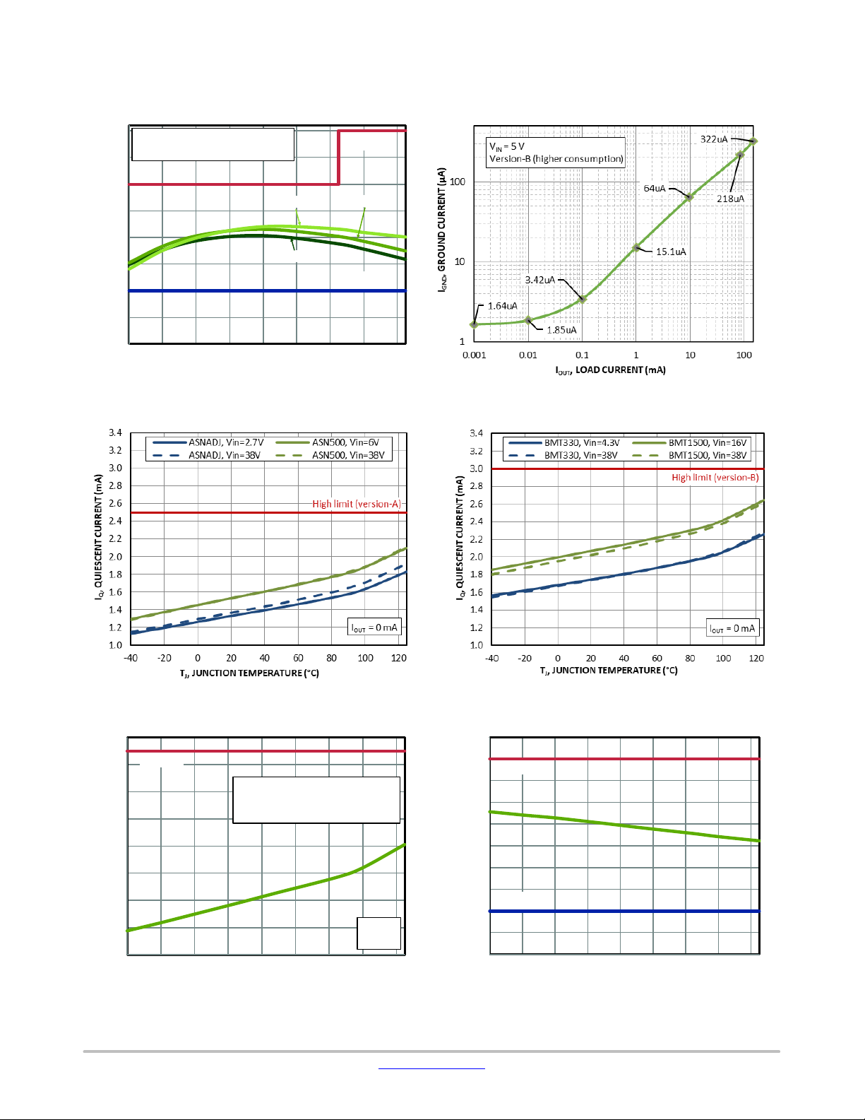
Figure 6. Output Voltage vs. Temperature Figure 7. Ground Current vs. Load
(NCP730−5.0V, Version−B)
Figure 8. Quiescent Current vs. Temperature
(Version−A)
1.6
High limit
1.4
A)
1.2
μ
(
SHDN
1.0
0.8
0.6
0.4
SHUTDOWN CURRENT, I
0.2
0.0
-40 -20 0 20 40 60 80 100
Note:
Shutdown current is measured at IN pin
and includes EN pin pull-up current.
JUNCTION TEMPERATURE, TJ(°C)
V
V
IN
EN
= 38 V
= 0 V
120
Figure 9. Quiescent Current vs. Temperature
(Version−B)
1.10
1.05
High limit
(V)
1.00
EN -TH
0.95
0.90
0.85
0.80
0.75
Low limit
0.70
ENABLE THRESHOLD VOLTAGE, V
0.65
0.60
-40 -20 0 20 40 60 80 100
JUNCTION TEMPERATURE, TJ(°C)
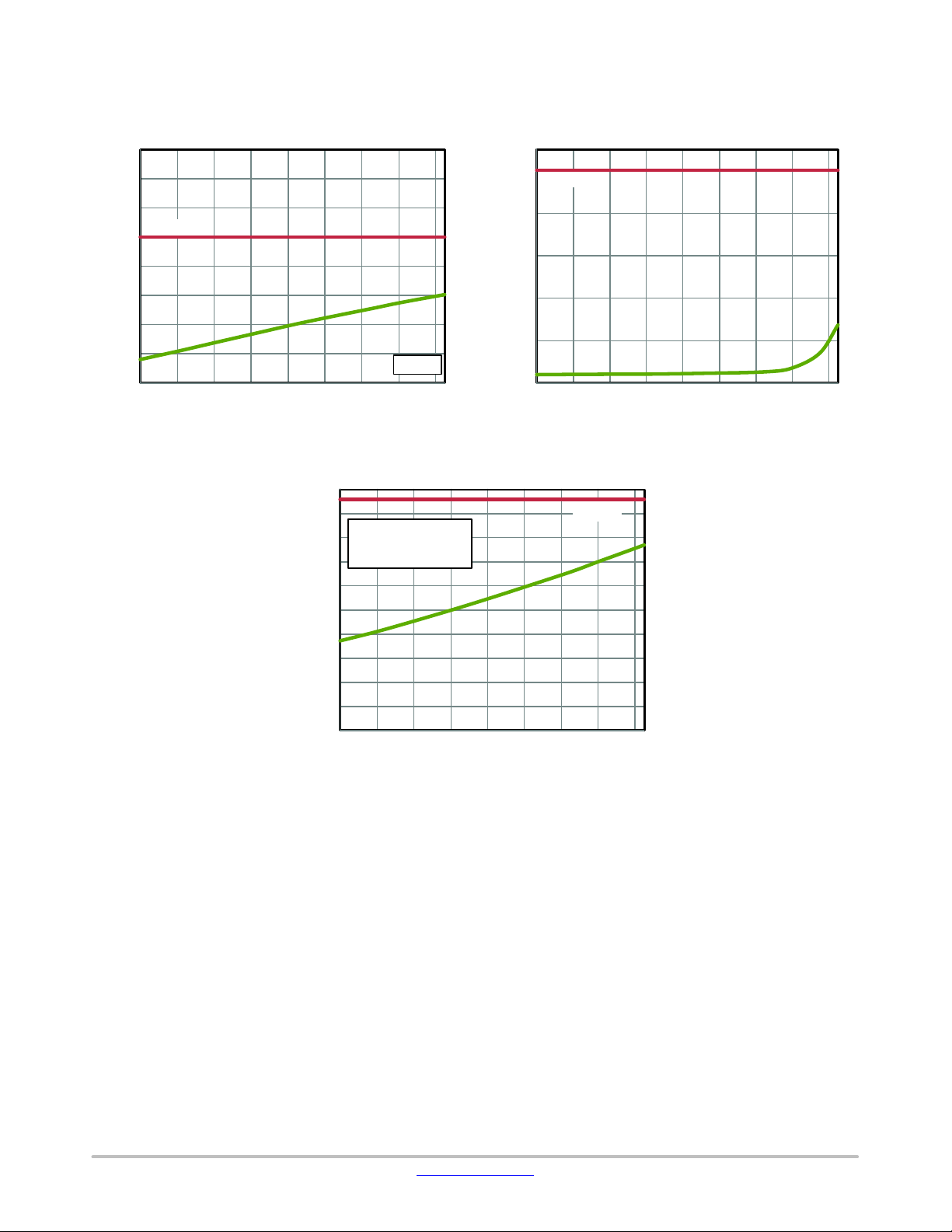
Figure 10. Shutdown Current vs. Temperature Figure 11. Enable Threshold Voltage vs.
Temperature
120
www.onsemi.com
6
VIN = V
1.6
1.4
A)
μ
(
1.2
EN-PU
1.0
0.8
OUT−NOM
High limit
TYPICAL CHARACTERISTICS
+ 1 V and VIN ≥ 2.7 V, VEN = 1.2 V, I
= 1 mA, C
OUT
NCP730
= 1.0 mF, ADJ tied to OUT, TJ = 25°C, unless otherwise specified
OUT
A)
μ
(
0.10
High limit
0.08
ADJ
0.06
0.6
0.4
ENABLE PULL- UP CURRENT, I
0.2
0.0
-40 -20 0 20 40 60 80 100
TEMPERATURE (°C)
Figure 12. Enable Internal Pull−Up Current vs.
Temperature
500
450
V
= V
OUT
400
(mV)
350
DROP
300
250
200
150
100
DROPOUT VOLTAGE, V
= 150 mA
I
OUT
All output voltage versions
50
0
-40 -20 0 20 40 60 80 100
Figure 14. Dropout Voltage vs. Temperature
VEN= 1 V
120
- 100 mV
OUT-NOM
JUNCTION TEMPERATURE, TJ(°C)
0.04
0.02
ADJ INPUT CURRENT, I
0.00
-40 -20 0 20 40 60 80 100
TEMPERATURE (°C)
Figure 13. ADJ Input Current vs. Temperature
High limit
120
120
www.onsemi.com
7
VIN = V
OUT−NOM
TYPICAL CHARACTERISTICS
+ 1 V and VIN ≥ 2.7 V, VEN = 1.2 V, I
= 1 mA, C
OUT
NCP730
= 1.0 mF, ADJ tied to OUT, TJ = 25°C, unless otherwise specified
OUT
4.3 V
150 mA
1 mA
+58 mV
3.3 V
-120 mV
C1: V
IN
(ac) 50 mV/div
C2: V
OUT
C4: I
OUT
1.0 V/div 20.0 ms/div
100 mA/div
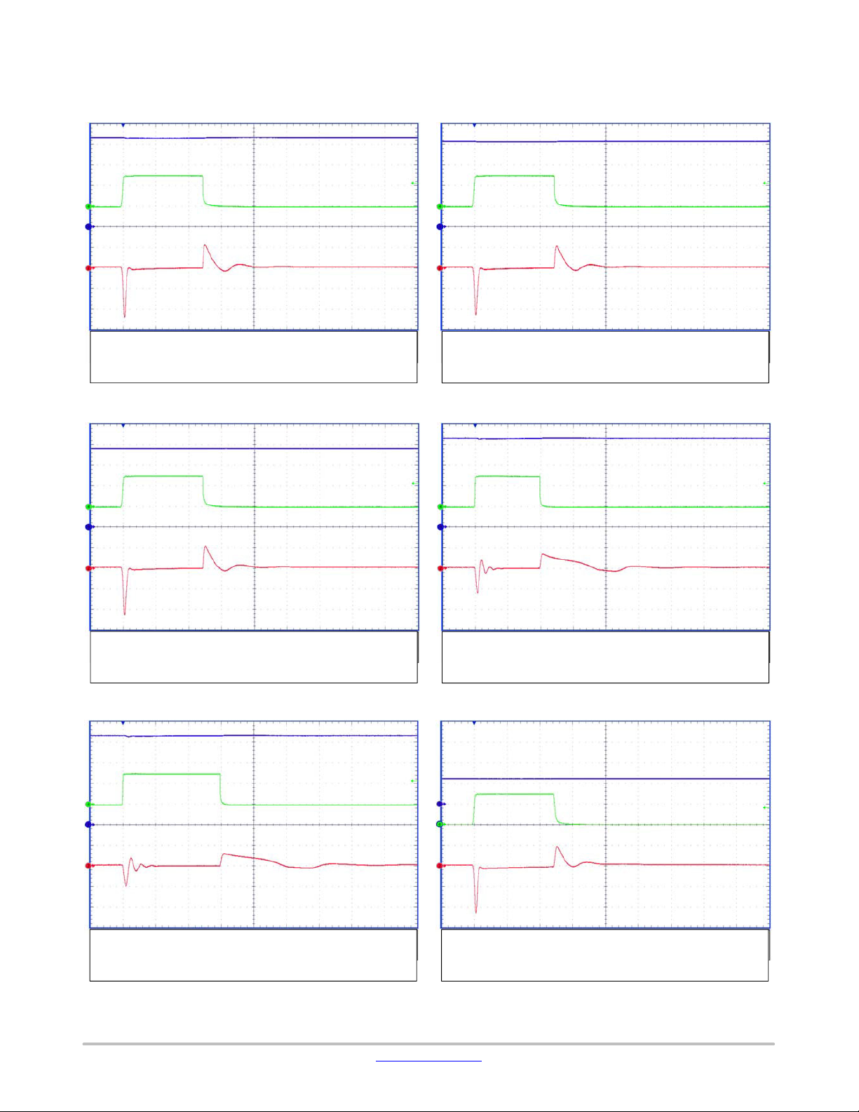
Figure 15. Load Transient − NCP730−3.3 V,
C
= 1 mF
OUT
38.0 V
150 mA
1 mA
+58 mV
3.3 V
V
IN
8.3 V
V
IN
150 mA
I
OUT
1 mA
I
OUT
+55 mV
V
OUT
3.3 V
V
OUT
-115 mV
C1: V
IN
C2: V
(ac) 50 mV/div
OUT
C4: I
OUT
2.0 V/div 20.0 ms/div
100 mA/div
Figure 16. Load Transient − NCP730−3.3 V,
C
= 1 mF
OUT
V
IN
4.3 V
V
IN
150 mA
I
OUT
1 mA
I
OUT
+37 mV
V
OUT
3.3 V
V
OUT
-120mV
C1: V
C2: V
C4: I
IN
OUT
OUT
(ac) 50 mV/div
10.0 V/div 20.0 ms/div
100 mA/div
Figure 17. Load Transient − NCP730−3.3 V,
C
= 1 mF
OUT
4.3 V
150 mA
1 mA
3.3 V
-50 mV
+30 mV
C1: V
IN
C2: V
(ac) 50 mV/div
OUT
C4: I
OUT
Figure 19. Load Transient − NCP730−3.3 V,
1.0 V/div 50.0 ms/div
100 mA/div
C
= 22 mF
OUT
-60 mV
C1: V
IN
C2: V
(ac) 50 mV/div
OUT
C4: I
OUT
1.0 V/div 50.0 ms/div
100 mA/div
Figure 18. Load Transient − NCP730−3.3 V,
C
= 10 mF
OUT
V
IN
V
IN
I
OUT
I
OUT
6.0 V
150 mA
1 mA
+55 mV
V
OUT
5.0 V
V
OUT
-115 mV
C1: V
IN
C2: V
(ac) 50 mV/div
OUT
C4: I
OUT
5.0 V/div 20.0 ms/div
100 mA/div
Figure 20. Load Transient − NCP730−5.0 V,
C
= 1 mF
OUT
www.onsemi.com
8
VIN = V
OUT−NOM
TYPICAL CHARACTERISTICS
+ 1 V and VIN ≥ 2.7 V, VEN = 1.2 V, I
= 1 mA, C
OUT
NCP730
= 1.0 mF, ADJ tied to OUT, TJ = 25°C, unless otherwise specified
OUT
38.0 V
150 mA
1 mA
+48 mV
5.0 V
-112 mV
C1: V
IN
C2: V
(ac) 50 mV/div
OUT
C4: I
OUT
10.0 V/div 20.0 ms/div
100 mA/div
Figure 21. Load Transient − NCP730−5.0 V,
C
= 1 mF
OUT
6.0 V
150 mA
1 mA
V
IN
6.0 V
V
IN
150 mA
I
OUT
V
OUT
1 mA
5.0 V
+36 mV
I
OUT
V
OUT
-60mV
C1: V
IN
(ac) 50 mV/div
C2: V
OUT
C4: I
OUT
5.0 V/div 50.0 ms/div
100 mA/div
Figure 22. Load Transient − NCP730−5.0 V,
C
= 10 mF
OUT
V
15.5 V
IN
V
IN
150 mA
I
OUT
1 mA
I
OUT
5.0 V
+34 mV
-53 mV
C1: V
IN
(ac) 50 mV/div
C2: V
OUT
C4: I
OUT
5.0 V/div 50.0 ms/div
100 mA/div
Figure 23. Load Transient − NCP730−5.0 V,
C
= 22 mF
OUT
38.0 V
150 mA
1 mA
15.0 V
+50 mV
-110 mV
C1: V
IN
(ac) 100 mV/div
C2: V
OUT
C4: I
OUT
10.0 V/div 20.0 ms/div
100 mA/div
V
OUT
15.0 V
+55 mV
V
OUT
-120 mV
C1: V
IN
(ac) 100 mV/div
C2: V
OUT
C4: I
OUT
10.0 V/div 20.0 ms/div
100 mA/div
Figure 24. Load Transient − NCP730−15.0 V,
C
= 1 mF
OUT
V
IN
V
15.5 V
IN
150 mA
I
OUT
1 mA
I
OUT
+40 mV
V
OUT
15.0 V
V
OUT
-105 mV
C1: V
IN
(ac) 50 mV/div
C2: V
OUT
C4: I
OUT
10.0 V/div 50.0 ms/div
100 mA/div
Figure 25. Load Transient − NCP730−15.0 V,
C
= 1 mF
OUT
Figure 26. Load Transient − NCP730−15.0 V,
www.onsemi.com
9
C
OUT
= 10 mF

VIN = V
mA
00mA
mA
= 1
00mA
OUT−NOM
TYPICAL CHARACTERISTICS
+ 1 V and VIN ≥ 2.7 V, VEN = 1.2 V, I
= 1 mA, C
OUT
NCP730
= 1.0 mF, ADJ tied to OUT, TJ = 25°C, unless otherwise specified
OUT
15.5 V
150 mA
1 mA
+45 mV
15.0 V
-98 mV
C1: V
IN
(ac) 50 mV/div
C2: V
OUT
C4: I
OUT
10.0 V/div 50.0 ms/div
100 mA/div
Figure 27. Load Transient − NCP730−15.0 V,
C
= 22 mF
OUT
5.3 V
4.3 V
+3.5 mV
+2 mV
3.3 V
I=1
OUT
C
= 1
OUT
V
V
V
15.5 V
IN
V
IN
150 mA
I
OUT
1 mA
I
OUT
+16 mV
V
OUT
15.0 V
V
OUT
-44 mV
C1: V
IN
(ac) 20 mV/div
C2: V
OUT
C4: I
OUT
10.0 V/div 100.0 ms/div
100 mA/div
Figure 28. Load Transient − NCP730−15.0 V,
C
= 50 mF
OUT
I=1
OUT
μ
IN
OUT
F
C
5.3 V
4.3 V
+9.5 mV
+7 mV
3.3V
OUT
= 1
μ
F
V
IN
V
OUT
-2.5 mV
C1: V 2.0 V/div 50.0μs/div
IN
C2: V
(ac) 5 mV/div
OUT
-3 mV
-6 mV
C1: V 2.0 V/div 10.0
IN
C2: V
(ac) 10 mV/div
OUT
-8 mV
Figure 29. Line Transient − NCP730−3.3 V Figure 30. Line Transient − NCP730−3.3 V
9.3 V
8.3 V
+1 mV
-1 mV
C1: V 2.0 V/div 50.0μs/div
IN
C2: V
(ac) 5 mV/div
OUT
+1 m V
-1 mV
3.3 V
V
I=1
OUT
C
OUT
V
IN
μ
OUT
F
9.3 V
8.3 V
+2 mV
-2 mV
C1: V 2.0 V/div 10.0μs/div
IN
C2: V
(ac) 10 mV/div
OUT
+2 mV
-2 mV
Figure 31. Line Transient − NCP730−3.3 V Figure 32. Line Transient − NCP730−3.3 V
I=1
OUT
C
= 1
OUT
3.3 V
μ
V
V
s/div
IN
μ
F
OUT
www.onsemi.com
10

VIN = V
mA
00
mA
mA
47
00mA
C1: V
.0 V/div
OUT−NOM
TYPICAL CHARACTERISTICS
+ 1 V and VIN ≥ 2.7 V, VEN = 1.2 V, I
= 1 mA, C
OUT
NCP730
= 1.0 mF, ADJ tied to OUT, TJ = 25°C, unless otherwise specified
OUT
I=1
OUT
C
= 47 μF
3.3 V
OUT
V
IN
V
OUT
5.3 V
4.3 V
+0.7 mV
-0.5 mV
C1: V 2.0 V/div 50.0μs/div
IN
C2: V
(ac) 1 mV/div
OUT
+0.6 mV
-0.7 mV
4.3 V
5.3 V
+0.2 mV
-0.2 mV
C1: V 2.0 V/div 200.0μs/div
IN
C2: V
(ac) 1 mV/div
OUT
+0.2 m V
-0.2 mV
Figure 33. Line Transient − NCP730−3.3 V Figure 34. Line Transient − NCP730−3.3 V
8.3 V
9.3 V
I=1
OUT
C
=
OUT
V
IN
μ
F
9.3 V
8.3 V
I=1
OUT
C
= 47 μF
OUT
V
3.3 V
I=1
OUT
C
= 47μF
OUT
IN
V
OUT
V
IN
+0.1 mV
-0.1 mV
C1: V 2.0 V/div 20 0.0μs/div
IN
C2: V
(ac) 1 mV/div
OUT
+0.2 mV
-0.1 mV
3.3 V
V
OUT
+0.2 mV
-0.4 mV
C1: V 2.0 V/div 50.0μs/div
IN
C2: V
(ac) 1 mV/div
OUT
+0.4 mV
-0.2 mV
Figure 35. Line Transient − NCP730−3.3 V Figure 36. Line Transient − NCP730−3.3 V
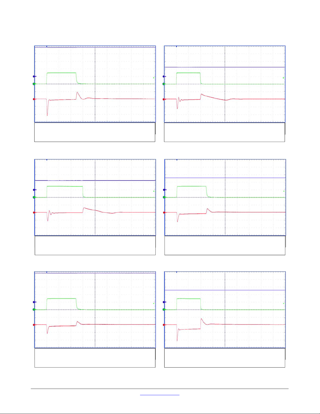
V = 38 V <-worst condition
IN
V
OUT
I is limited to I
OUT
down because T
C
OUT
discharge
current peak
level and slowly goes
OSC
rises and I
J
is TJdependent
OSC
Not shorted
I
OUT
Shorted => 0 V
C1: V 5.0 V/div 200.0μs/div
IN
C2: V
C3: V
OUT
OUT
500 mV/div
200 mA/div
I is limited to I
OUT
on/off because of thermal shutdown
V
OUT
IN
C2: V
OUT
C3: V
OUT
V = 38 V <- worst condition
IN
OSC
Shorted => 0 V
5
500 mV/div
200 mA/div
level and turned
3.3 V
Not shorted
5.0m
V
I
OUT
s/div
OUT
Figure 37. Output Short (1 ms) −
NCP730−ADJ−1.2 V
Figure 38. Output Short (20 ms) −
NCP730−ADJ−1.2 V
www.onsemi.com
11

VIN = V
OUT−NOM
TYPICAL CHARACTERISTICS
+ 1 V and VIN ≥ 2.7 V, VEN = 1.2 V, I
= 1 mA, C
OUT
NCP730
= 1.0 mF, ADJ tied to OUT, TJ = 25°C, unless otherwise specified
OUT
Figure 39. PSRR − NCP730−3.3 V, C
I
= 10 mA
OUT
OUT
= 1 mF,
Figure 41. PSRR − NCP730−3.3 V, VIN = 4.3 V,
I
= 100 mA
OUT
Figure 40. PSRR − NCP730−3.3 V, C
I
= 100 mA
OUT
Figure 42. PSRR − NCP730−3.3 V, V
I
= 100 mA
OUT
= 1 mF,
OUT
= 8.3 V,
IN
Rms Noise Value (10Hz - 100kHz) 229.1 230.6 225.2
ms Noise Value (10Hz - 1MHz)
R
Rms Noise Value (10Hz - 100kHz) 45.8 46.1 45.0
Rms Noise Value (10Hz - 1MHz) 45.9 46.2 45.1
Vi=6V Vi=12V Vi=36V
229.5 231.1 225.7
Vrms
m
Vrmsm
Vrms/Vm
Vrms/Vm
Figure 43. Noise – FIX − 5.0 V, I
C
= 1 mF, Different V
OUT
OUT
IN
= 1 mA,
www.onsemi.com
12
Rms Noise Value (10Hz - 100kHz) 230.6 240.2 226.3
Rms Noise Value (10Hz - 1MHz) 231.1 251.9 272.7
Rms Noise Value (10Hz - 100kHz)
Rms Noise Value (10Hz - 1MHz) 46.2 50.4 54.5
Io=1mA Io=10mA Io=150mA
46.1 48.0 45.3
Vrmsm
Vrmsm
Vrms/Vm
Vrms/Vm
Figure 44. Noise – FIX − 5.0 V, C
Different I
OUT
OUT
= 1 mF,

VIN = V
OUT−NOM
TYPICAL CHARACTERISTICS
+ 1 V and VIN ≥ 2.7 V, VEN = 1.2 V, I
= 1 mA, C
OUT
NCP730
= 1.0 mF, ADJ tied to OUT, TJ = 25°C, unless otherwise specified
OUT
Rms Noise Value (10Hz - 100kHz) 219.8 239.5 259.1
Rms Noise Value (10Hz - 1MHz) 219.9 239.8 263.9
ms Noise Value (10Hz - 100kHz)
R
Rms Noise Value (10Hz - 1MHz) 44.0 48.0 52.8
Io=1mA Io=10mA Io=150mA
44.0 47.9 51.8
Vrmsm
Vrmsm
Vrms/Vm
Vrms/Vm
Figure 45. Noise – FIX − 5.0 V,
C
= 1 mF + 10 mF, Different I
OUT
Rms Noise Value (10Hz - 100kHz) 240.2 239.5 222.2
Rms Noise Value (10Hz - 1MHz) 251.9 239.8 222.4
Rms Noise Value (10Hz - 100kHz) 48.0 47.9 44.4
Rms Noise Value (10Hz - 1MHz) 50.4 48.0 44.5
Co=1u Co=1u+10u Co=1u+50u
Vrmsm
Vrmsm
Vrms/Vm
Vrms/Vm
Figure 47. Noise – FIX − 5.0 V, I
Different C
OUT
= 10 mA,
OUT
OUT
Rms Noise Value (10Hz - 100kHz) 189.2 222.2 229.0 235.1 240.7
Rms Noise Value (10Hz - 1MHz) 189.3 222.4 229.2 235.3 241.0
Rms Noise Value (10Hz - 100kHz)
Rms Noise Value (10Hz - 1MHz) 37.9 44.5 45.8 47.1 48.2
Io=1mA Io=10mA Io=25mA Io=50mA Io=150mA
37.8 44.4 45.8 47.0 48.1
Figure 46. Noise – FIX − 5.0 V,
C
= 1 mF + 50 mF, Different I
OUT
Rms Noise Value (10Hz - 100kHz) 226.3 259.1 240.7
Rms Noise Value (10Hz - 1MHz) 272.7 263.9 241.0
Rms Noise Value (10Hz - 100kHz) 45.3 51.8 48.1
Rms Noise Value (10Hz - 1MHz)
Figure 48. Noise – FIX − 5.0 V, I
Co=1u Co=1u+10u Co=1u+50u
54.5 52.8 48.2
Different C
OUT
Vrmsm
Vrmsm
Vrms/Vm
Vrms/Vm
OUT
Vrmsm
Vrmsm
Vrms/Vm
Vrms/Vm
OUT
= 150 mA,
R
ms Noise Value (10Hz - 100kHz)
Rms Noise Value (10Hz - 1MHz)
Rms Noise Value (10Hz - 100kHz)
Rms Noise Value (10Hz - 1MHz)
NCP730ASNADJ-5V
Cff=10p Cff=100p Cff=1nF Cff=10nF
199.3 132.3 99.0 80.5 240.2
208.9 150.9 124.9 111.2 251.9
39.9 26.5 19.8 16.1 48.0
41.8 30.2 25.0 22.2 50.4
BMT500
Cff=NA
Vrmsm
Vrmsm
Vrms/Vm
Vrms/Vm
Figure 49. Noise – ADJ−set−5.0 V with
Different C
and FIX − 5.0 V
FF
Rms Noise Value (10Hz - 100kHz) 203.0 240.2 457.0
ms Noise Value (10Hz - 1MHz)
R
ms Noise Value (10Hz - 100kHz)
R
Rms Noise Value (10Hz - 1MHz) 64.9 50.4 30.9
www.onsemi.com
13
ASN330 BMT500 BMT1500
214.2 251.9 463.9
61.5 48.0 30.5
Figure 50. Noise – FIX, I
C
= 1 mF, Different V
OUT
Vrmsm
Vrmsm
Vrms/Vm
Vrms/Vm
= 10 mA,
OUT
OUT

NCP730
APPLICATIONS INFORMATION
Input Capacitor Selection (CIN)
Input capacitor connected as close as possible is necessary
to ensure device stability. The X7R or X5R capacitor should
be used for reliable performance over temperature range. The
value of the input capacitor should be 1 mF or greater (max.
value is not limited). This capacitor will provide a low
impedance path for unwanted AC signals or noise modulated
onto the input voltage. There is no requirement for the ESR
of the input capacitor but it is recommended to use ceramic
capacitor for its low ESR and ESL. A good input capacitor
will limit the influence of input trace inductance and source
resistance during load current changes. When a large load
transients (like 1 mA to 150 mA) happens in the application
the input power source of the LDO needs to provide enough
power and the input voltage must not go below the level
defined by this equation: V
= V
IN
OUT−NOM
+ V
DO
otherwise the output voltage drop will be significantly
higher (because LDO will enter the dropout state). In some
cases when power supply powering the LDO has a poor load
transient response or when there is a long connection
between LDO and its power source then capacitance of input
capacitor needs to be high enough to cover the LDO’s input
voltage drop caused by load transient and maintains its value
above the V
IN
= V
OUT−NOM
+ VDO level (then CIN could be
in range of hundreds of mF).
Output Capacitor Selection (C
OUT
)
The LDO requires the output capacitor connected as close
as possible to the output and ground pins. The LDO is
designed to remain stable with output capacitor’s effective
capacitance in range from 1 mF to 100 mF and ESR from
1 mW to 200 mW. The ceramic X7R or X5R type is
recommended due to its low capacitance variations over the
specified temperature range and low ESR. When selecting
the output capacitor the changes with temperature and DC
bias voltage needs to be taken into account. Especially for
small package size capacitors such as 0402 or smaller the
effective capacitance drops rapidly with the applied DC bias
voltage (refer the capacitor’s datasheet for details). Larger
capacitance and lower ESR improves the load transient
response and PSRR.
Output Voltage
NCP730 is available in two version from output voltage
point of view. One is fixed output voltage version (FIX
version) and the other one is adjustable output voltage
version (ADJ version).
The ADJ version has ADJ pin, which could be connected
to the OUT pin directly, just to compensate voltage drop
across the internal bond wiring and PCB traces or could be
connected to the middle point of the output voltage resistor
divider for adjustment. When it is connected to the OUT pin
the output voltage of the circuit is simply the same as the
nominal output voltage of the LDO. At this case, without
ADJ resistor divider, the LDO should be loaded by at least
200 nA (by the application or added pre−load resistor).
When connected to the resistor divider the output voltage
could be computed as the ADJ reference voltage (1.2 V)
multiplied by the resistors divider ratio, see following
equation.
V
OUT
+ V
ADJ
@ǒ1 )
1
Ǔ
) I
@ R
R
ADJ
2
(eq. 1)
1
R
Where:
V
is output voltage of the circuit with resistor divider.
OUT
V
is the LDO’s ADJ reference voltage.
ADJ
I
is the LDO’s ADJ pin input current.
ADJ
R
and R2 are resistors of output resistor divider.
1
At the classical “old style” regulators like LM317 etc. the
resistors where small (100 W − 10 kW) to make regulator
stable at light loads (divider was also a pre−load function).
On NCP730, which is very low quiescent current LDO
regulator (1 mA), we need to care about current consumption
of surrounding circuitry so we need to set the current through
resistor divider flowing from V
through R1 and R2 to
OUT
GND, as low as possible.
On the other hand, the parasitic leakage current flowing
into ADJ pin (I
I
⋅ R1). The I
ADJ
) causes V
ADJ
is temperature dependent so it is
ADJ
voltage error (given by
OUT
changing and we cannot compensate it in application, we
just can minimize the influence by setting of R
value low,
1
what is in opposite to maximizing its value because of
current consumption.
So when selecting the R
compromise between desired V
and R2 values we need to find a
1
error (temperature
OUT
dependent) and total circuit quiescent current.
If we want to simplify this task, we can say the I
be 100−times higher than I
range. If we chose the ratio “I
more than 100 as stated before), the ΔV
I
change over temperature would be lower and opposite,
ADJ
to I
if the ratio “I
In limited T
R2
J
” is smaller, the error would be bigger.
ADJ
temperature range −40°C to +85°C the I
at expected TJ temperature
ADJ
to I
R2
” higher (for example
ADJ
error caused by
OUT
should
R2
ADJ
is about 10−times smaller than in the full temperature range
−40°C to +125°C (see typical characteristics graph of I
ADJ
over temperatures), so we can use bigger R1, R2 values, as
could be seen at next examples.
Example 1:
Desired V
voltage is 5.0 V. Computed maximal TJ in
OUT
application (based on max. power dissipation and cooling)
is 85°C. Than I
at 85°C is about: I
ADJ
ADJ85
= 10 nA.
www.onsemi.com
14

NCP730
OUT
VOUT =5V
R1
3.76 MW
NCP730A ADJ
GND
ADJ
VR2=V
10nA
1.2V
I
R
R1
1.01uA
I
R2
1uA
2
V
5V
I
ADJ
ADJ
COUT
1mF
OUT
1.2 MW
Figure 51. ADJ Output Voltage Schematic − Example 1
We chose:
IR2+ 100 @ I
+ 100 @ 10E−9 + 1 mA
ADJ85
Then:
V
R2
R2
R1
R1
+
+
1.2
1E−6
V
OUT
I
ADJ85
+
1.01E−6
+ 1.2 MW
* V
R2
) I
R2
3.8
+ 3.762 MW
5 * 1.2
+
10E−9 ) 1E−6
R2+
R1+
I
V
I
Verification:
@ǒ1 )
= 25°C) the I
J
R
1
Ǔ
) I
R
2
3.762E6
1.2E6
Ǔ
ADJ
) 1E−9 @ 3.762E6
For low temperature (T
V
+ V
ADJ
+ 1.2 @ǒ1 )
V
OUT
OUT
+ 4.966 V
For maximal temperature (TJ = 85°C) the I
V
OUT
+ 1.2 @ǒ1 )
+ 5.000 V
3.762E6
1.2E6
Ǔ
) 10E−9 @ 3.762E6
ADJ25
@ R
1
ADJ85
= 1 nA:
= 10 nA:
Output voltage error for temperatures 85°C to 25°C is:
DV
OUT
+
V
* V
OUT85
V
OUT85
5.000 * 4.966
+
OUT25
5.000
@ 100
@ 100 + 0.68%
Total circuit quiescent current at TJ = 25°C is:
I
Q(TOT)
+ I
) IR1+ 1.3E−6 ) 1.01E−6 + 2.31 mA
Q(LDO)
We can see that current consumption of external resistor
divider is almost the same as quiescent current of LDO.
Example 2:
Desired V
voltage is 5.0 V. Computed maximal TJ in
OUT
application (based on max. power dissipation and cooling)
is in this case higher, 125°C, to show the difference. Than
maximal I
at 125°C is I
ADJ
= 100 nA (based on
ADJ125
Electrical characteristics table).
OUT
VOUT =5V
R1
376 kW
NCP730A ADJ
GND
ADJ
VR2=V
I
100nA
ADJ
1.2V
I
R
R1
10.1uA
I
R2
10uA
2
V
5V
ADJ
COUT
1mF
OUT
120kW
Figure 52. ADJ Output Voltage Schematic − Example 2
We chose:
IR2+ 100 @ I
+ 100 @ 100E−9 + 10 mA
ADJ125
Then:
V
R2
R1
+
+
1.2
10E−6
V
OUT
I
ADJ125
+
10.1E−6
+ 120 kW
* V
R2
) I
3.8
+
100E−9 ) 10E−6
R2
+ 376.2 kW
5 * 1.2
R2+
R1+
I
R2
V
I
R1
Verification:
For low temperature (T
V
+ V
ADJ
+ 1.2 @ǒ1 )
V
OUT
OUT
+ 4.962 V
For maximal temperature (TJ = 125°C) the I
V
+ 1.2 @ǒ1 )
OUT
+ 5.000 V
@ǒ1 )
= 25°C) the I
J
R
ADJ1
Ǔ
R
ADJ2
376.2E3
376.2E3
120E3
120E3
Ǔ
Ǔ
= 1 nA:
ADJ25
) I
@ R
ADJ
ADJ1
) 1E−9 @ 376.2E3
= 100 nA:
ADJ125
) 100E−9 @ 376.2E3
Output voltage error for temperatures 125°C to 25°C is:
DV
OUT
+
V
* V
OUT125
V
OUT125
5.000 * 4.962
+
OUT25
5.000
@ 100
@ 100 + 0.76%
Total circuit quiescent current at TJ = 25°C is:
I
+ I
Q(TOT)
We can see that error of V
in example 1 (because we have used the same “I
) IR1+ 1.3E−6 ) 10.1E−6 + 11.4 mA!!!
Q(LDO)
voltage is almost the same as
OUT
R2
to I
ADJ
ratio = 100x) but the application quiescent current is almost
10−times higher (because of 10−times higher divider
current).
CFF Capacitor
Even the NCP730 is very low quiescent current device,
both the load transients over/under shoots and settling times
are excellent. See the Typical characteristics graphs.
”
www.onsemi.com
15

At adjustable application, the external resistor divider
with input ADJ pin capacity and ADJ pin PCB trace capacity
to GND makes a low pass filter what negatively affects the
dynamic behavior of the LDO. On the next picture is shown
how this unwanted side effect could be compensated by
adding of feed−forward capacitor C
OUT
NCP730A ADJ
1.2V
GND
ADJ
across R1 resistor.
FF
R1
2M4
2
R
CFF
1nF
OUT=5V
V
COUT
1mF
750k
Figure 53. ADJ Output Voltage Schematic − C
Capacitor
FF
The value of the CFF depends on R1 and R2 resistor values.
When R
C
, R2 values are in hundreds of kiloohms, proposed
1
value is 1 nF, as shown on picture above, for the best
FF
dynamic performance. Generally, the value could be in
range from 0 to 10 nF.
On next three pictures is shown the C
capacitor
FF
influence to dynamic parameters.
NCP730
Figure 56. PSRR – Different C
FF
=1−to−150mA – 100mA/div
I
OUT
CFF=0pF
C
= 100p
FF
C
=1nF
FF
V
V
=3.3V – 50mV/div
OUT
N
set to 3.3V
CFF=10pF
Figure 54. Load Transient – Different C
N
set to 3.3V
V
= 0´
IN
CFF=0pF
V
=3.3V – 1V/div
OUT
= 100pF
C
FF
=1nF
C
FF
=4.3V – 1V/div
IN
CP730ASN−ADJ
Time – 10ms/div
FF
CP730ASN−ADJ
38V − 5V/div
Time – 2ms/div
Figure 57.
Startup
In the NCP730 device there are two main internal signals
which triggers the startup process, the under−voltage
lockout (UVLO) signal and enable signal. The first one
comes from UVLO comparator, which monitors if the IN
pin voltages is high enough, while the second one comes
from EN pin comparator. Both comparators have embedded
hysteresis to be insensitive to input noise.
Not only the comparator but also the pull−up current
source is connected to EN pin. Current source is sourcing
I
= 300 nA current flowing out of the chip what
EN-PU
ensures the level on the pin is high enough when it is left
floating. The comparator compares the EN pin voltage with
internal reference level 0.9 V (typ.). Hysteresis is 100 mV
(typ.).
The UVLO comparator threshold voltage is 1.95 V (typ.)
and hysteresis is 200 mV (typ.).
Figure 55. Startup Timing – Different C
FF
www.onsemi.com
16

NCP730
EN
IN
300 nA
1.95 V
= 300 nA
EN −PU
I
0.9 V
V
C CEN
93% of V
UVLO Comparator
V−REFERENCE
AND SOFT−START
EN Comparator
THERMAL
SHUTDOWN
PG Comparator
R EF
UVLO
Enable
V
1.2V
R EF
Current limit
EA
VFB=1.2V
DEGLITCH
DELAY TMR
OUT
RADJ1
ADJ
RADJ2
GND
PG
NC
Figure 58. Internal Block Diagram – EN Pin
Startup by IN Pin Voltage
When the LDO is started by IN pin voltage rise, it is turned
ON when the voltage is higher than UVLO threshold level.
This is the case of both following application circuits, the
first one with EN pin floating and the second one with EN
pin connected to IN pin.
When the EN pin is floating (left unconnected) its voltage,
after the LDO is powered, rises to V
(2.5 V – 4.5 V, V
pulls the pin voltage up. V
dependent) as the internal current source
IN
voltage level on EN pin is
CCEN
CCEN
level
higher than EN comparator threshold so the LDO is turned
ON.
IN
V
IN
C
1
mF
V
IN
NCP730
EN
EN
GND
OUT
C
1mF
VOUT
OUT
VIN VOUT
C
IN
1mF1mF
IN
NCP730
V
EN
EN
GND
OUT
OUT
C
Figure 61. Circuit – EN Pin Connected to IN Pin
V
IN−TOP
V
IN
V
IN−TOP
= V
V
EN
IN
V
OUT−NOM
V
OUT
t
START
V
IUL−TH
V
– V
IUL−TH
V
EN−TH
V
– V
EN−TH
95% of V
Time
IUL−HY
EN−HY
OUT−NOM
Figure 62. Startup Timing – EN Pin Connected to IN
Pin
Startup time in both cases above is measured from the
point where IN pin voltage reaches V
IUL−TH
value to point
when OUT pin voltage reaches 95% of its nominal value.
The reason why the LDO is started by the UVLO signal
and not by the enable signal is the fact that the UVLO signal
turns to valid state later then the enable. (EN pin voltage
reaches the V
V
Startup by EN Pin Voltage
IUL-TH
level).
level prior the IN pin voltage reaches the
EN-TH
When VIN voltage in the application is settled above the
V
the level higher than V
lower than (V
reaches V
level and control voltage to the EN pin is applied,
IUL-TH
enables the LDO and the level
EN−TH
EN-TH
– V
EN-HY
) disables it.
Startup time is measured from point where V
value to point when V
EN−TH
voltage reaches
OUT
voltage
EN
95% of its nominal value.
Figure 59. Circuit – Floating EN Pin
V
IN−TOP
V
IN
V
V
EN
V
OUT
CCEN
V
OUT−NOM
t
START
V
IUL−TH
V
– V
IUL−TH
V
EN−TH
V
– V
EN−TH
95% of V
Time
IUL−HY
EN−HY
OUT−NOM
Figure 60. Startup Timing – Floating EN Pin
It is also possible to connect EN pin directly to IN pin in
the whole input voltage range. The startup sequence is very
similar to previous case, the only difference is that the EN
pin voltage is not clamped to V
as V
voltage.
IN
level but it is the same
CCEN
www.onsemi.com
17
VIN
C
1mF
IN
V
EN
IN
EN
NCP730
GND
Figure 63. Circuit – LDO Controlled by V
V
IN
V
EN
V
OUT−NOM
V
OUT
t
START
Figure 64. Timing – VEN−Startup
OUT V OUT
COUT
1mF
EN
V
IUL−TH
V
– V
IUL−TH
V
EN−TH
V
EN−TH
95% of V
Time
– V
IUL−HY
EN−HY
OUT−NOM

NCP730
Startup by IN Pin Voltage − Delayed
The startup time triggered by IN pin voltage rise could be
delayed by adding of EN pin capacitor (C
sequence is following − after the V
charging of C
(I
) is started. When the CEN capacitor voltage (V
EN-PU
capacitor by internal pull−up current
EN
voltage is applied, the
IN
reaches EN comparator’s threshold voltage (V
LDO is enabled. Charging of C
continues up to the V
EN
). The startup
EN
EN−TH
CEN
) the
CCEN
level (2.5 V – 4.5 V, VIN dependent) with no following effect.
The steepness of the LDO’s output voltage rise (soft−start
time) is not affected by using of C
additional delay time (t
t
CEN−DELAY
+ CEN@
The total startup time (t
CEN−DELAY
V
EN−TH
I
EN−PU
START-CEN
) could be computed by:
+ CEN@
capacitor is a sum of normal startup time (t
additional delay time caused by C
(t
CEN-DELAY
):
t
START−CEN
+ t
START
) t
capacitor. The
EN
0.9 V
300 nA
(eq. 2)
) with connected C
) and
START
capacitor
EN
CEN−DELAY
(eq. 3)
EN
Value of the CEN capacitor could be in range from 0 to
several microfarads. Capacitor’s leakage current must be
negligible to internal pull−up current I
charging will be affected and adding of R
, otherwise the
EN−PU
resistor from IN
EN
to EN pin will be needed.
EN−TH
COUT
1mF
VOUT
OUT−NOM
V IN
C
1mF
C EN
IN
IN
V
EN
I
EN−PU
EN
NCP730
GND
OUT
Figure 65. Circuit – CEN−Delayed VIN−Startup
V
IN
START
V
V
(with C
CCEN
OUT−NOM
)
EN
(without CEN)
V
EN
V
OUT
(without C
t
CEN−DELAY
(with C
)
EN
t
START−CEN
)
EN
t
Figure 66. Timing – CEN−Delayed VIN−Startup
Startup by Transistor at EN Pin
V
95% of V
Time
If the LDO needs to be controlled by transistor or
generally by open collector / open drain circuit as shown at
the next picture, the control behavior is inverted. High
control signal makes the EN pin voltage low and low control
signal makes it high because the transistor is connected as
signal invertor.
In this application we need to care about transistor’s
leakage current which must be negligible compared to the
internal pull−up current I
)
additional pull−up resistor R
maximum value of the EN resistor R
= 300 nA otherwise
EN−PU
will be needed. The
EN
EN-MAX
from maximal external transistor leakage current (over
desired temperature range) I
voltage V
IN−MIN
:
R
EN−MAX
T- LK -M A X
+
I
T−LK−MAX
and minimal input
V
IN−MIN
For safe, select the EN resistor value REN lower enough
to computed R
When R
EN
EN-MAX
is used the overall application shutdown
.
current is increased because the current through R
(I
) is added to input shutdown current of the LDO
REN
(I
SD(LDO)
(I
SD(TOT)
Where V
(given by R
). The total application shutdown current
) is:
I
SD(TOT)
is the drain to source voltage of the transistor
T−DS
DSON
I
REN
and I
+ I
+
REN
SD(LDO)
ǒ
VIN* V
).
) I
REN
Ǔ
T−DS
R
EN
The overall application quiescent current when R
used is influenced only by the transistor’s leakage current
I
.
T−LK
I
+ I
Q(TOT)
VIN
C
1mF
V
IN
CTRL
I
Q(TOT)
REN
Opt.
I
Q(LDO)
I
I
I
REN
V
EN−PU
T
IN
EN
EN
Figure 67. Circuit – EN Pin Controlled by Transistor
V
CTRL
V
EN
V
OUT−NOM
V
OUT
t
START
Figure 68. Startup Timing – EN Pin Controlled by
Transistor
Q(LDO)
NCP730
) I
GND
T−LK
OUT
is computed
(eq. 4)
resistor
EN
(eq. 5)
(eq. 6)
C
OUT
1mF
V
EN−TH
V
– V
EN−TH
EN−HY
95% of V
Time
OUT−NOM
EN
is
VOUT
www.onsemi.com
18

NCP730
V
CTRL
V
OUT
V
EN
V
CCEN
V
OUT−NOM
V
EN−TH
(without CEN)
t
CEN−DELAY
t
START−CEN
t
START
(without CEN)
(with C
EN
)
(with C
EN
)
95% of V
OUT−NOM
Time
Startup by Transistor at EN Pin − Delayed
The startup time triggered by EN pin voltage rise, could
be delayed the same way as IN pin triggered startup, by
adding of C
– when the external NMOS control voltage (V
the C
EN
and LDO is disabled. After the V
charging of C
source (I
(V
, which is the VEN in fact) reaches EN comparator’s
CEN
threshold voltage (V
C
then continues up to the V
EN
V
dependent) with no following effect. The steepness of
IN
capacitor. The startup sequence is following
EN
) is high
CTRL
capacitor connected to the EN pin is shorted to GND
is turned low the
CTRL
capacitor by the internal pull−up current
EN
) starts. When the CEN capacitor voltage
EN-PU
) the LDO is enabled. Charging of
ENTH
level (2.5 V – 4.5 V,
CCEN
the LDO’s output voltage rise (soft−start time) is not affected
by using of C
(t
CEN-DELAY
delayed startup time with C
3. What has been said about the C
capacitor. The additional delay time
EN
) could be computed by eq. 2 and the total
capacitor (t
EN
START-CEN
capacitor selection at
EN
) by eq.
previous paragraphs is applicable here as well.
UVLO threshold value, the external resistor divider from IN
pin to EN pin, is needed.
Note that the specification of EN pin threshold voltage
(0.7 V to 1.05 V over full operating temperature range) is
not as precise as threshold voltage on dedicated UVLO
devices. The reason is the EN circuit has to have ultra−low
current consumption (NCP730 I
while I
is 300 nA typ. so EN comparator is powered
EN−PU
is 350 nA typ. even
SHDN
by less than 50 nA typ.). We need to count with that when
thinking about the IN pin UVLO design. Below is the
application example to show what precision we can get.
VIN
C
1mF
CEN
100pF
Optional
I
Q(TOT)
IN
REN1
REN2
I
Q(LDO)
I
I
I
REN1
V
EN−PU
REN2
IN
NCP730
EN
EN
GND
OUT
C
OUT
1mF
VOUT
Also in this application we need to care about transistor’s
leakage current which must be negligible compared to the
internal pull−up current I
additional pull−up resistor R
EN
and computations as stated in previous paragraph about R
= 300 nA otherwise
EN−PU
will be needed. Same rules
EN
are applicable here. Note that REN would influence the speed
of C
capacitor charging.
EN
I
CTRL
CIN
1mF
Q(TOT)
VIN
V
Figure 69. Circuit – EN Pin with CEN Controlled by
REN
Opt.
I
Q(LDO)
I
REN
V
I
EN−PU
EN
C
IN
EN
EN
Transistor
NCP730
GND
OUT
VOUT
COUT
1mF
Figure 71. Circuit – IN Voltage UVLO by EN Pin
The two main equations for IN pin threshold computation
are:
V
+
+
I
REN1
IN−UVLO−TH
V
R
EN1
R
EN2
I
EN−TH
) I
EN−PU
REN1
* V
EN−TH
(eq. 7)
From that, we can get:
V
IN−UVLO−TH
+ V
EN−TH
@ǒ1 )
R
EN1
Ǔ
* R
R
EN2
EN1
@ I
(eq. 8)
EN−PU
We can see that IN pin UVLO threshold is EN pin
threshold multiplied by the resistor divider ratio as expected
but it is unwillingly affected by I
the I
to choose the I
I
EN-PU
choose I
current could vary up to the 1 mA max., we need
EN-PU
current several times higher to make the
REN1
influence negligible. The good practice could be to
at least 10−times higher than I
REN1
pull−up current. As
EN-PU
EN-PU
(the
bigger the better for the accuracy).
An optional component in this application is C
capacitor.
EN
Its main function is filtering out the spurious signals coming
from IN power supply and the minor function is to delay the
startup as described in section before. The value of C
EN
for
filtering purpose could be in range from 10 pF to 10 nF. The
time constant of this filter is given by:
R
@ R
EN1
) I
) R
REN1
EN2
EN2
t
+ CEN@
FILTER
Figure 70. Startup Timing – EN Pin with C
Controlled by Transistor
Enable Input as Inaccurate IN Pin UVLO
The EN input pin on NCP730 device is specified by
threshold voltage and hysteresis both with minimum and
maximum value, what allows using EN comparator as
adjustable input voltage UVLO function. To set the V
EN
power consumption. At no load state, the quiescent current
I
than I
IN
www.onsemi.com
19
The side effect of the UVLO divider is increased overall
of the application is:
Q(TOT)
I
Q(TOT)
So if we select the I
EN-PU-MAX
REN1
(1 mA), then the UVLO divider current is
R
EN1
+ I
Q(LDO)
value at least 10−times higher
(eq. 9)
(eq. 10)

NCP730
almost 10-times higher than typical LDO’s quiescent
current (1.3 mA).
IN voltage UVLO application example:
Desired V
voltage is 5 V, the LDO’s input voltage in
OUT
normal state is 12 V. We want to turn−off the LDO’s output
voltage when input voltage is below 10 V (max.).
First, choose the I
I
current:
EN-PU
I
+ 10 @ I
REN1
Then, to obtain R
V
IN-UVLO-TH
V
EN-TH
= 10 V, we need to put maximum value of
(1.05 V) and minimum value of I
the equations for R
V
R
EN1
R
EN2
The resulting V
V
V
IN−UVLO−TH−MAX
IN−UVLO−TH
+
+
I
REN1
IN−UVLO−TH−MIN
V
IN−UVLO−TH−MIN
V
IN−UVLO−TH−MAX
I
Q(TOT)
V
EN−TH
) I
IN-UVLO-TH
+ V
+ V
+ I
Q(LDO)
When higher I
current as 10−times the maximum
REN1
+ 10 @ 1 mA + 10 mA
EN−PU
EN1
I
REN1
EN−PU
EN1
and R
−V
EN−TH
and R
+
10 mA ) 0 mA
values for maximal
EN2
EN-PU
:
EN2
10 V−1.05 V
+
10 mA
1.05
limits will be:
R
EN1
R
895 kW
105 kW
+ 5.77 V
R
R
895 kW
105 kW
+ 10.0 V
Ǔ
* R
EN2
Ǔ
* 895 kW @ 1 mA
EN1
Ǔ
* R
EN2
Ǔ
−895 kW @ 0 mA
EN−TH−MIN
V
REN1
@ǒ1 )
+ 0.7 @ǒ1 )
V
IN−UVLO−TH−MIN
EN−TH−MAX
@ǒ1 )
+ 1.05 @ǒ1 )
IN−UVLO−TH−MAX
) I
+ 1.3 mA ) 10 mA + 11.3 mA
REN1
is selected the V
(eq. 11)
(0 mA) into
(eq. 12)
+ 895 kW
+ 105 kW
(eq. 13)
@ I
EN1
EN−PU−MAX
@ I
EN1
EN−PU−MIN
IN-UVLO-TH-MIN
would be slightly near the target value, the
V
IN-UVLO-TH-MAX
would stay the same but the I
Q(TOT)
would be significantly higher:
I
REN1
+ 100 @ I
+ 100 @ 1 mA + 100 mA
EN−PU
(eq. 14)
We would get:
(eq. 15)
I
Q(TOT)
+ I
V
Q(LDO)
R
+ 89.5 kW
EN1
R
+ 10.5 kW
EN2
IN−UVLO−TH−MIN
) I
+ 1.3 mA ) 100 mA + 101.3 mA
REN1
+ 6.58 V
We can see the IN pin UVLO threshold precision
computed above (5.77 V or 6.58 V min. / 10.0 V max.) is not
too high because the EN pin threshold and EN pin internal
pull−up current specifications are not so tight as on
dedicated UVLO devices but at some applications this
precision could fit the needs.
Output Current Limit
Output current is internally limited to 280 mA typ. The
LDO will source this current when the output voltage drops
down from the nominal output voltage (test condition is 90%
of V
OUT−NOM
). If the output voltage is shorted to ground,
the device continues with current limitation at the same
current level. The current limit and short circuit protection
will work properly over the whole temperature and input
voltage ranges. There is no limitation for the short circuit
duration.
Minimal output current limit value is 200 mA what could
be used to cover current demand peaks, higher than the
LDO’s nominal output current (150 mA).
Inrush Current
At every application, the startup sequence needs a special
care because during power−up the bypass capacitors
connected to the power rail are charged from zero to input
voltage level, what generates a current spike, so called
inrush current. The size of such current spike depends on the
voltage transient slope (the faster the bigger spike), on the
total impedance of the loop from the power source to bypass
capacitor (traces impedance, power source internal
impedance and capacitor impedance; the lower the bigger
spike) and on the capacitor value (the higher the bigger
spike).
This inrush current during startup could cause power
source’s overcurrent event, damage of PCB traces, power
line fuses blowing or spurious signal generation in
surrounding application parts.
For a simplified case when total impedance between input
power source and bypass capacitor is zero, we can use
following equation to compute the inrush current, based just
on voltage transient slope (dV/dt) and the capacitor value:
i
INRUSH
+ C @
dV
dt
(eq. 16)
Example – when the voltage changes from 0 V to 24 V in
10 ms and bypass capacitor is 10 mF, the inrush current is:
i
INRUSH
+ 10 mF @
24 V * 0V
10 ms
+ 24A
(eq. 17)
Of course, this is the worst case when impedances in the
circuit are zero, but it shows why we need to care about
startup and what defines the inrush current value. We can see
the inrush current is lower when capacitance and voltage
change are smaller or transition time is longer.
In most cases, the capacitor value and the input voltage
change are defined by the application so then the only thing
we can do is to slow down the input voltage transition time.
We can do it directly by changing input voltage rise time by
soft−start circuit (related to Equation 16) or indirectly by
adding a current limit block, which in combination with the
capacitor will do the same (slower the input voltage rise), see
the following equation:
t
START
+ C @
dV
I
LIMIT
(eq. 18)
www.onsemi.com
20

NCP730
EA
0.9
VFB=1.2V
I
EN−PU
= 300nA
V
CCEN
1.95 V
1.2V
RADJ2
RADJ1
93 % of V
REF
We see that voltage transition time (t
START
) is given by
bypass capacitor value (C), by the voltage change (dV) and
by current limit value (I
) of added current limit block.
LIMIT
Now back to LDO application. Here we can see two
different inrush current spikes. The first one is caused by the
LDO’s input capacitor (C
) charging from zero to the input
IN
voltage level. It happens when the previous power block (for
example DC/DC) starts providing the input voltage to the
LDO circuit. The maximum level of this inrush current is
given by Equation 16. It doesn’t matter if LDO is enabled or
disabled as this inrush current spike is related only to C
and it can’t be suppressed by the LDO, it is matter of
previous power block. This inrush current spike is shown at
Figure 73, point (1).
The second inrush current spike is generated by the LDO’s
output capacitor (C
) charging from zero to nominal
OUT
output voltage level. It happens when the LDO is enabled by
any way (by driving EN pin or by internal UVLO when EN
pin is connected to IN pin). This inrush current is limited by
the LDO’s soft−start and current limit functions.
Soft−start function limits the speed of the output voltage
rise to avoid possible latch−up of application circuit caused
by high dV/dt what naturally suppresses input inrush current
(related to Equation 16).
The current limit function, used to guard the LDO and
application against the overcurrent, is also used during the
LDO’s startup to limit the input inrush current.
Now focus onto the NCP730 device. At the next picture
we can see both, soft−start and current limit functions have
been implemented, shown in red. At this device, the startup
current limit level is the same as the normal operation
current limit level (specified at the parametric table).
IN
EN
A few practical notes. If the LDO’s output capacitor value
is small (for example 1 mF), then soft−start limited output
V−REFERENCE
AND SOFT−START
V
UVLO Comparator
UVLO
Enable
EN Comparator
THERMAL
SHUTDOWN
PG Comparator
Figure 72.
V
REF
DEGLITCH
DELAY TMR
Current limit
voltage rise is slow enough to suppress the inrush current
(output capacitor charging current, generated by dV
based on Equation 16, is significantly smaller than the
OUT
ADJ
GND
OUT
PG
NC
IN
/dt,
current limit value). While at the case of big output capacitor
(for example 47 mF), the soft−start time is not slow enough
and the input current needs to be limited by the current limit
function.
Next picture shows both startup cases – with small (1 mF)
and big (47 mF) output capacitors. Startup is caused by IN
voltage rise, EN pin is connected to IN pin and device
voltage version is 5.0 V.
(3)
(1)
= 10μs
R
(2)
1μF
1μF
47μF
47μF
I
IN
V
IN
V
OUT
V, t
0³6
C1: V 1.0V/div 200μs/div
IN
C2: V
C4: I
OUT
IN
1.0V/div
200mA/div
Figure 73.
With the C
= 1 mF, the inrush current (seen at I
OUT
IN
signal at point−2) is almost zero, its level is defined by
soft−start time which is about 550 ms (from the picture).
DV
@
t
START
550 ms
OUT
(eq. 19)
+ 9mA
i
INRUSH−1mF
With the C
i
OUT
+ C
INRUSH
+ 1 mF @
OUT
5V* 0V
= 47 mF, the inrush current should be
47−times higher than in case of 1 mF:
i
INRUSH−47mF
+ 47 mF @
5V* 0V
500 ms
+ 470 mA
(eq. 20)
Therefore, in this case the current limit is activated and
limits the C
charging current to about 280 mA (from the
OUT
picture, point−3). This leads to enlarging of startup time to:
DV
@
OUT
I
LIMIT
+ 870 ms
(eq. 21)
t
START
t
+ C
START
+ 47 mF @
OUT
5V* 0V
270 mA
One additional thing could be seen at the picture above
and it is a small current spike highlighted as a point−1 at the
I
curve. It is the inrush current caused by input voltage
IN
transient (from 0 V to 6 V in 10 ms) and input capacitor
= 100 nF. As stated before, for this current spike is
C
IN
responsible the prior power source, not the LDO (in this case
the test equipment which generates the V
C
inrush current amplitude is:
IN
i
INRUSH_POINT−1
+ 100 nF @
6V* 0V
10 ms
transient). The
IN
+ 60 mA
(eq. 22)
www.onsemi.com
21

NCP730
Power Supply Rejection Ratio
The LDO features high power supply rejection ratio even
it is very low quiescent current device. See the Typical
characteristics section for the graphs over different
conditions.
The PSRR at higher frequencies (from about 100 kHz) can
be tuned by the selection of C
capacitor, applied input
OUT
voltage and proper PCB layout (minimizing impedance
from load to C
PG Output
OUT
).
Version B of the NCP730 device contains PG circuit for
the V
voltage level monitoring. Internally it is combined
OUT
from PG comparator, deglitch/delay timer and output
NMOS transistor (highlighted by red color at picture
below). At both, ADJ and FIX versions, the PG comparator
compares internal feedback signal voltage (V
93% of V
(typ.) what makes the function independent to
REF
) with the
FB
the output voltage absolute value (it always compares set
V
with 93% of its nominal value).
OUT
If PG is used at ADJ device version and CFF capacitor is
used as well, then C
must be small enough (10 − 33 pF
FF
when R1, R2 are in range of hundreds of kilo ohms)
otherwise the PG output will show ”power ok state” sooner
than the output voltage reaches the PG threshold value. It is
because the C
slows down the output voltage rise time
FF
while ADJ pin voltage, what is the PG comparator input,
remains fast. Note that any AC voltage change at OUT pin
goes into ADJ pin through the C
of C
in fact − to speed up regulator reactions), but for PG
FF
(what is the main reason
FF
operation it makes this kind of issue that voltage at ADJ pin
is already on the target level (V
) while OUT voltage is
REF
still rising. This issue is a natural behavior for any adjustable
regulator so it is not an issue just for this particular device.
IN
EN
1.95 V
V
= 300 nA
EN −PU
I
0.9 V
CCEN
AND SOFT−START
93% of V
UVLO Comparator
V−REFERENCE
EN Comparator
THERMAL
SHUTDOWN
PG Comparator
R EF
UVLO
Enable
V
R EF
1.2V
Current limit
EA
VFB=1.2V
DEGLITCH
DELAY TMR
OUT
RADJ1
ADJ
RADJ2
GND
PG
NC
The PG output turns into high impedance state (Hi−Z) to
show “power ok state” when the V
the PG threshold level (V
(t
fail state” when the V
after deglitch time (t
) and turns into short to GND level to show “power
PG−DLY
OUT
PG−DG
+ V
PG-TH
falls below the level (V
).
The PG threshold voltage is 93% of V
the hysteresis is 2% of V
OUT-NOM
voltage rises above
OUT
) after delay time
PG−HY
OUT-NOM
(typ.).
PG-TH
(typ.) and
Because the PG output is open drain type it needs to be
connected by external pull resistor to a voltage level, which
defines the PG pin voltage at time when it is in Hi−Z state.
It allows connections of PG pin to circuit with the same or
different power supply voltage to the LDO’s V
OUT
level.
Below are the connections examples.
5.0V
C
OUT
mF
1
Output
5.0V
C
OUT
mF
1
3.3V
VCC
PG
R
Application
PGI
CTRL
VCCA
Appl.
Part 1
(analog)
VCCD
R
PG
PGI
CTRL
Appl.
Part 2
(MCU)
GND
OUT
PG
IN
NCP730B500
EN
Figure 75. Circuit Example – PG Connected to LDO’s
IN
OUT
NCP730B500
EN
GND
PG
Figure 76. Circuit Example – PG Connected to
Application Power Supply
Following timing diagrams show the situation when LDO
falls out of regulation 3 times (output voltage drops down
from nominal value) because of (for example) insufficient
IN pin voltage.
Note that the V
voltage where the R
is in Hi−Z state and just R
V
level. In the first example when RPG is connected to
PG
LDO’s output, the V
the drops. In the second example the R
LDO independent power rail (3.3 V) so the V
voltage at “power ok state” follows the
PG
is connected because the PG output
PG
connection point defines the
PG
follows the LDO’s V
PG
PG
including
OUT
is connected to
is not
PG
following the LDO’s output voltage.
)
Blue objects are valid for ADJ version
Note:
Green objects are valid for FIX version
Red objects are valid for B version (with PG)
Figure 74. Power Good Output Block Diagram
www.onsemi.com
22

t
V
Time
region
< t
OUT−LOW
PG−DGtPG−DG
5V
OUT
5V
V
PG
21 3
t
PG−DLY
V
– V
PG−TH
V
PG−TH
~10kW (t~500ns)
R
PG
~100kW (t~5ms)
R
PG
Time
4
PG−HY
Figure 77. Timing – PG Connected to LDO’s Output
t
V
Time
region
OUT
3.3V
V
< t
OUT−LOW
PG−DGtPG−DG
5V
PG
21
3 4
t
PG−DLY
V
– V
PG−TH
V
R
R
PG−HY
PG−TH
~10kW (t~500ns)
PG
~100kW (t~5ms)
PG
Time
Figure 78. Timing – PG Connected to Application
Power Supply 3.3 V
The timing diagrams have been divided into 4 time
regions to show different situations:
In region−1, the V
drop is not deep enough so the PG
OUT
output shows “power ok state”.
In region−2, the V
V
threshold level but the duration of the drop is shorter
PG-TH
then PG deglitch time (t
drop is deeper and crosses the
OUT
= 160 ms typ.) so the PG
PG-DG
output still shows “power ok state”. Note that the deglitch
time has been intentionally implemented to filter out
spurious output voltage drops (caused for example by fast
load transients etc.).
In both two first regions the V
voltage level where the R
(V
LDO(OUT)
In region−3, the V
duration is longer then t
or V
CCD
).
drop is deep enough and the
OUT
PG-DG
is high and follows the
PG
resistor is connected to
PG
deglitch time so the PG output
is shorted to GND pin and shows power fail state.
In region−4, the V
When it crosses the level (V
returns back to its nominal value.
OUT
PG-TH
– V
) the PG output
PG-HY
turns from short to GND into Hi−Z state, not immediately,
but after the PG delay time (t
PG-DLY
= 320 ms typ.). The PG
delay ensures that low PG pulse, showing “power fail state”,
is always longer than the t
time and then could be
PG-DLY
caught by the application circuit (for example by MCU).
NCP730
RPG Value Selection
As shown on the Figure 77 and Figure 78 in the time
region-4, the steepness of PG signal return to high level
depends on the R
capacitance of LDO’s PG output, parasitic capacitance of
PG signal PCB traces and the application circuit PGI input
capacitance. The lower RPG resistance the faster PG return
to high level.
At the most applications, the PG return speed to high level
is not a concern, mainly because of the fact that the LDO
already delays the PG return by the t
typ.) intentionally so the returning speed itself is negligible.
The next view to the R
at “power fail state” when the current from the supply flows
through the R
of the power fail state so probably not a concern too.
At the electrical characteristics table we can find the
parameter “PG Output Low Level Voltage (V
defines the drop across the PG internal transistor when it
sinks current 1 mA. We can take this current condition
(1 mA) as a maximal PG current (I
computation (as we know the PG drop at this level, 0.4 V
max.). If the application input current I
I
we can compute the R
RPG
And, for example, when RPG is connected to 3.3 V power
rail:
R
PG−MIN
NCP730B
Figure 79. Circuit Example for RPG Value Selection
From the opposite side, RPG is limited to its maximum
value, based on: maximum PG leakage current
I
PG−LK−MAX
input V
, maximum threshold voltage of the application
PGI−TH−MAX
leakage current I
R
PG−MAX
For example, when RPG is connected to 3.3 V power rail,
max. threshold voltage of the application input is 1.3 V and
application input leakage current is 3 mA max.:
pull−up resistance (with relation to
PG
PG-DLY
value is the power consumption
PG
to the grounded PG pin. This is just a case
PG
PG−MAX
) for the R
PGI
R
PG−MIN
+
V
CC−RPG
I
PG−MAX
PGI−MIN
+
V
R
PG
V
CC−RPG
I
PG−MAX
+
CC−RPG
by:
3.3 V
1mA
I
RPG
+ 3.3 kW
Application
I
PG
V
PG
I
PGI
Note: IPG = I
RPG
PGI
when I
PG
GND
and maximum application input
PGI−LK−MAX
V
CC−RPG
+
I
PG−LK−MAX
. Then:
* V
PGI−TH−MAX
) I
PGI−LK−MAX
time (320 ms
)” which
PG-OL
PG−MIN
is negligible to
(eq. 23)
(eq. 24)
= 0mA
PGI
(eq. 25)
www.onsemi.com
23

NCP730
OUT
0V
IN
IN
= 50 Ohm
PG
PG
DO
OUT
IN
R
PG−MAX
V
CC−RPG
+
I
PG−LK−MAX
3.3 V * 1.3 V
+
1 mA ) 3 mA
* V
) I
+ 500 kW
PGI−TH−MAX
PGI−LK−MAX
(eq. 26)
Based on results above, the RPG value could be selected
in range from 3.3 kW to 500 kW to fit the example
application.
PG and OUT Pin Voltages during Startup/Shutdown
At the picture below an example of NCP730BMT500
measured startup waveform is shown. EN pin was shorted
to IN pin, PG output was connected to OUT pin by resistor
R
= 10 kOhm, OUT was loaded by R
PG
C
and C
IN
were 1 mF both. Slow input voltage rise and
OUT
LOAD
= 50 Ohm,
fall times have been used to show LDO’s overall behavior.
At the point 0 the input voltage starts to rise from 0 to 6 V,
LDO is in shutdown (because V
threshold) and output voltage is 0 V. At the point 1 the V
is below its UVLO
IN
IN
voltage reaches UVLO threshold level and LDO starts
charging of output capacitor. V
by internal soft−start function. At the point 2 the V
rising speed is defined
OUT
OUT
voltage reaches almost the VIN voltage as it rises faster and
LDO gets into dropout. The difference between V
V
is the dropout voltage VDO as shown in the zoomed
OUT
window. At the point 3 the V
PG hysteresis level (V
of V
OUT−NOM
) and from this point LDO counts the power
good delay time (t
PG−TH
). This delay time prolongs the low
PG−DLY
reaches PG threshold plus
OUT
+ V
= 93% + 2% = 95%
PG−HY
IN
and
state of PG signal for easier detection of power fault (it
defines minimum PG low time in fact). After this delay, the
PG pin rises to high level showing that V
point 4 the V
starts to be higher than (V
reaches its nominal value (5.0 V) as the V
OUT
OUT−NOM
+ VDO) and LDO gets
into regulation where it stays until point 5, where the V
is ok. At the
OUT
IN
IN
starts to be too low and LDO returns to dropout again. At the
point 6 the V
of V
OUT−NOM
deglitch time (t
drops below the PG threshold level (93%
OUT
) and LDO starts counting the power good
) which filters fast V
PG−DG
undershoots
OUT
(caused for example by line/load transient responses). After
this delay, the PG output is shorted to 0 V level to highlight
“power fail” state. At the point 7, the V
voltage is lower
IN
than input voltage UVLO threshold minus UVLO hysteresis
level and LDO goes into the shutdown state.
100 mA
I
0mA
Zoom
V
3
0V
V
V
V
1
2
V
V
4
0
C1: V 1.0V/div 500.0μs/div
IN
C2: V
C3: V
C4: I
1.0V/div
OUT
1.0V/div
PG
100mA/div
IN
5.0V
6.0V
t
PG-DLY
t
PG-DG
R
LOAD
C
6
5
= 1 μF
OUT
= 10 kOhm
R
7
Figure 80. Startup/Shutdown Example − NCP730BMT500
www.onsemi.com
24

NCP730
Thermal Shutdown
When the LDO’s die temperature exceeds the thermal
shutdown threshold value the device is internally disabled.
The IC will remain in this state until the die temperature
decreases by the thermal shutdown hysteresis value. Once
the IC temperature falls this way, the LDO is back enabled.
The thermal shutdown feature provides the protection
against overheating due to some application failure and it is
not intended to be used as a normal working function.
Power Dissipation
Power dissipation caused by voltage drop across the LDO
and by the output current flowing through the device needs
to be dissipated out from the chip. The maximum power
dissipation is dependent on the PCB layout, number of used
Cu layers, Cu layers thickness and the ambient temperature.
The maximum power dissipation can be computed by
following equation:
P
D(MAX)
+
TJ* T
q
JA
A
+
125 * T
q
JA
A
[W]
(eq. 27)
Where: (TJ − TA) is the temperature difference between the
junction and ambient temperatures and θ
is the thermal
JA
resistance (dependent on the PCB as mentioned above).
For reliable operation junction temperature should be less
than +125°C.
The power dissipated by the LDO for given application
conditions can be calculated by the next equation:
PD+ VIN@ I
Where: I
)ǒVIN* V
GND
is the LDO’s ground current, dependent on the
GND
OUT
Ǔ
@ I
[W]
OUT
(eq. 28)
output load current.
Connecting the exposed pad and NC pin to a large ground
planes helps to dissipate the heat from the chip.
The relation of θ
JA
and P
D(MAX)
to PCB copper area and
Cu layer thickness could be seen on the Figures 81 and 82.
Figure 81. qJA and P
Figure 83. Maximum Output Current vs. Input
Voltage
vs. Copper Area Figure 82. qJA and P
D(MAX)
www.onsemi.com
25
vs. Copper Area
D(MAX)
Figure 84. Maximum Output Current vs. Input
Voltage

NCP730
PCB Layout Recommendations
To obtain good LDO’s stability, transient performance
and good regulation characteristics place C
IN
and C
OUT
capacitors as close as possible to the device pins and make
the PCB traces wide, short and place capacitors to the same
layer as the LDO is (to avoid connection through vias). The
same rules should be applied to the connections between
C
and the load – the less parasitic impedance the better
OUT
transients and regulation at the point of load.
To minimize the solution size, use 0402 or 0201 capacitor
sizes with appropriate effective capacitance in mind.
Regarding high impedance ADJ pin, prevent capacitive
coupling of the trace to any switching signals in the circuitry.
Adequate input power filtering is always a good practice.
For load transients the input capacitor value must be high
enough to cover the current demands especially if the power
source is connected by long traces/wires with high
impedance.
Demo Boards
Below are the main part of the schematics and top/bottom
board layout pictures of the NCP730 demo boards for
various packages. These boards have been used during
evaluation to capture the data shown in this datasheet like:
transients, PSRR, startups etc. At some of these pictures are
shown details of PCB traces surrounding the LDO including
C
, C
IN
C
FF
, resistor divider R1/R2, feed forward capacitor
OUT
and IN/OUT−FORCE/SENSE connections.
Generally, when testing LDOs dynamic performance on
demo board which is connected to laboratory power supply
typically by long cables, the device needs additional input
capacitor. This capacitor covers the voltage drop generated
by the load current transients at the impedance of long
connection cables (note this is very different to normal
application where the distance of the LDO to its power
source is short).
Besides the LDO application circuit, each demo board
includes some supporting staff, the same at all boards:
• Positions for optional through hole SMB connectors at
IN, OUT and EN pins (Molex 73100−0258 or
compatible) mainly for line/load transients, PSRR,
noise and startup testing the demo board includes.
• Edge connector where all these signal leads too (the
appropriate receptacle type is SAMTEC
MECF−20−01−L−DV−WT).
• Thermal management circuit (heating transistor and
diodes as temperature sensors).
Figure 85. Edge Connector Pinout (All Demo Boards)
Figure 86. Thermal Circuit (All Demo Boards)
www.onsemi.com
26

NCP730
NCP730ASN/BSN (TSOP−5 package) Demo Board (2 layer PCB, rev. 1)
Figure 87. TSOP−5 Demo Board (2 layer, rev. 1) – Schematics (Main Part)
Figure 88. NCP730 Demo Board (2 layer, rev. 1) –
PCB Top Layer
Figure 90. TSOP−5 Demo Board (2 layer, rev. 1) – PCB Top Layer, Zoomed, Added Signal Labels
Figure 89. TSOP−5 Demo Board (2 layer, rev. 1) –
PCB Bottom Layer
www.onsemi.com
27

NCP730
NCP730AMT/BMT (WDFN−6 2x2 package) Demo Board (2 layer PCB, rev. 1)
Figure 91. WDFN−6 2x2 Demo Board (2 layer, rev. 1) – Schematics (Main Part)
Figure 92. WDFN−6 2x2 Demo Board (2 layer, rev. 1) –
PCB Top Layer
Figure 94. WDFN−6 2x2 Demo Board (2 layer, rev. 1) – PCB Top Layer, Zoomed, Added Signal Labels
Figure 93. WDFN−6 2x2 Demo Board (2 layer, rev. 1) –
PCB Bottom Layer
www.onsemi.com
28

NCP730
ORDERING INFORMATION
Part Number Marking Voltage Option (V
NCP730ASNADJT1G HAA ADJ
NCP730ASN250T1G HAC 2.5 V
NCP730ASN280T1G HAD 2.8 V
NCP730ASN300T1G HAF 3.0 V
NCP730ASN330T1G HAE 3.3 V
NCP730ASN500T1G HAG 5.0 V
NCP730BMTADJTBG MA ADJ
NCP730BMT250TBG MC 2.5 V
NCP730BMT280TBG MD 2.8 V
NCP730BMT300TBG ME 3.0 V
NCP730BMT330TBG MF 3.3 V
NCP730BMT500TBG MG 5.0 V
NCP730BMT1500TBG MH 15.0 V
*To order other package, voltage version or PG / non PG variant, please contact your ON Semiconductor sales representative.
OUT−NOM
) Version Package Shipping
Without PG
With PG
TSOP−5
(Pb−Free)
WDFN6 2x2
(Pb−Free)
3000 / Tape & Reel
3000 / Tape & Reel
www.onsemi.com
29

MECHANICAL CASE OUTLINE
PACKAGE DIMENSIONS
5
1
SCALE 2:1
NOTE 5
2X
2X
T0.10
B
A
54
B
123
G
A
T0.20
TOP VIEW
0.05
H
SIDE VIEW
D
0.205XC AB
S
C
SEATING
C
PLANE
CASE 483
K
J
END VIEW
TSOP−5
ISSUE N
DETAIL Z
M
DETAIL Z
DATE 12 AUG 2020
NOTES:
1. DIMENSIONING AND TOLERANCING PER ASME
Y14.5M, 1994.
2. CONTROLLING DIMENSION: MILLIMETERS.
3. MAXIMUM LEAD THICKNESS INCLUDES LEAD FINISH
THICKNESS. MINIMUM LEAD THICKNESS IS THE
MINIMUM THICKNESS OF BASE MATERIAL.
4. DIMENSIONS A AND B DO NOT INCLUDE MOLD
FLASH, PROTRUSIONS, OR GATE BURRS. MOLD
FLASH, PROTRUSIONS, OR GATE BURRS SHALL NOT
EXCEED 0.15 PER SIDE. DIMENSION A.
5. OPTIONAL CONSTRUCTION: AN ADDITIONAL
TRIMMED LEAD IS ALLOWED IN THIS LOCATION.
TRIMMED LEAD NOT TO EXTEND MORE THAN 0.2
FROM BODY.
MILLIMETERS
DIM MIN MAX
A
2.85 3.15
B
1.35 1.65
C 0.90 1.10
D 0.25 0.50
G 0.95 BSC
H 0.01 0.10
J 0.10 0.26
K 0.20 0.60
M 0 10
__
S 2.50 3.00
SOLDERING FOOTPRINT*
1.9
0.95
0.037
1.0
0.039
*For additional information on our Pb−Free strategy and soldering
details, please download the ON Semiconductor Soldering and
Mounting Techniques Reference Manual, SOLDERRM/D.
0.074
0.028
0.7
2.4
0.094
SCALE 10:1
ǒ
inches
mm
GENERIC
MARKING DIAGRAM*
5
XXXAYWG
G
1
Analog
XXX = Specific Device Code
A = Assembly Location
Y = Year
W = Work Week
G = Pb−Free Package
(Note: Microdot may be in either location)
Ǔ
*This information is generic. Please refer to
device data sheet for actual part marking.
Pb−Free indicator, “G” or microdot “ G”,
may or may not be present.
5
XXX MG
G
1
Discrete/Logic
XXX = Specific Device Code
M = Date Code
G = Pb−Free Package
DOCUMENT NUMBER:
DESCRIPTION:
ON Semiconductor and are trademarks of Semiconductor Components Industries, LLC dba ON Semiconductor or its subsidiaries in the United States and/or other countries.
ON Semiconductor reserves the right to make changes without further notice to any products herein. ON Semiconductor makes no warranty, representation or guarantee regarding
the suitability of its products for any particular purpose, nor does ON Semiconductor assume any liability arising out of the application or use of any product or circuit, and specifically
disclaims any and all liability, including without limitation special, consequential or incidental damages. ON Semiconductor does not convey any license under its patent rights nor the
rights of others.
© Semiconductor Components Industries, LLC, 2018
98ARB18753C
TSOP−5
Electronic versions are uncontrolled except when accessed directly from the Document Repository.
Printed versions are uncontrolled except when stamped “CONTROLLED COPY” in red.
PAGE 1 OF 1
www.onsemi.com

MECHANICAL CASE OUTLINE
PACKAGE DIMENSIONS
SCALE 4:1
PIN ONE
REFERENCE
6X
NOTE 4
0.10 C
0.10 C
0.05 C
0.05 C
DETAIL A
D
TOP VIEW
DETAIL B
SIDE VIEW
D2
1
A
B
A1
E
A3
A
A1
L
3
C
SEATING
PLANE
WDFN6 2x2, 0.65P
CASE 511BR
ISSUE B
A3
ALTERNATE B−2ALTERNATE B−1
DETAIL B
ALTERNATE
CONSTRUCTIONS
L
L1
ALTERNATE A−2ALTERNATE A−1
DETAIL A
ALTERNATE
CONSTRUCTIONS
DATE 19 JAN 2016
MOLD CMPDEXPOSED Cu
L
NOTES:
1. DIMENSIONING AND TOLERANCING PER ASME
Y14.5M, 1994.
2. CONTROLLING DIMENSION: MILLIMETERS.
3. DIMENSION b APPLIES TO PLATED TERMINAL AND
IS MEASURED BETWEEN 0.15 AND 0.25 mm FROM
THE TERMINAL TIP.
4. COPLANARITY APPLIES TO THE EXPOSED PAD AS
WELL AS THE TERMINALS.
5. FOR DEVICES CONTAINING WETTABLE FLANK
OPTION, DETAIL A ALTERNATE CONSTRUCTION
A-2 AND DETAIL B ALTERNATE CONSTRUCTION
B-2 ARE NOT APPLICABLE.
MILLIMETERS
DIMAMIN MAX
0.70 0.80
A1 0.00 0.05
A3 0.20 REF
b 0.25 0.35
D 2.00 BSC
D2 1.50 1.70
2.00 BSC
E
E2
0.90 1.10
e
0.65 BSC
L
0.20 0.40
L1
--- 0.15
GENERIC
MARKING DIAGRAM*
1
XX M
6
e
BOTTOM VIEW
DOCUMENT NUMBER:
DESCRIPTION:
E2
4
b
6X
M
M
0.05 C
98AON55829E
WDFN6 2X2, 0.65P
A0.10 C
B
NOTE 3
XX = Specific Device Code
M = Date Code
*This information is generic. Please refer to
device data sheet for actual part marking.
Pb−Free indicator, “G” or microdot “ G”,
may or may not be present.
RECOMMENDED
MOUNTING FOOTPRINT
1.72
1.12
PACKAGE
OUTLINE
6X
Electronic versions are uncontrolled except when accessed directly from the Document Repository.
Printed versions are uncontrolled except when stamped “CONTROLLED COPY” in red.
1
0.40
DIMENSIONS: MILLIMETERS
6X
0.45
0.65
PITCH
2.30
PAGE 1 OF 1
ON Semiconductor and are trademarks of Semiconductor Components Industries, LLC dba ON Semiconductor or its subsidiaries in the United States and/or other countries.
ON Semiconductor reserves the right to make changes without further notice to any products herein. ON Semiconductor makes no warranty, representation or guarantee regarding
the suitability of its products for any particular purpose, nor does ON Semiconductor assume any liability arising out of the application or use of any product or circuit, and specifically
disclaims any and all liability, including without limitation special, consequential or incidental damages. ON Semiconductor does not convey any license under its patent rights nor the
rights of others.
© Semiconductor Components Industries, LLC, 2019
www.onsemi.com

ON Semiconductor and are trademarks of Semiconductor Components Industries, LLC dba ON Semiconductor or its subsidiaries in the United States and/or other countries.
ON Semiconductor owns the rights to a number of patents, trademarks, copyrights, trade secrets, and other intellectual property. A listing of ON Semiconductor’s product/patent
coverage may be accessed at www.onsemi.com/site/pdf/Patent−Marking.pdf
ON Semiconductor makes no warranty, representation or guarantee regarding the suitability of its products for any particular purpose, nor does ON Semiconductor assume any liability
arising out of the application or use of any product or circuit, and specifically disclaims any and all liability, including without limitation special, consequential or incidental damages.
Buyer is responsible for its products and applications using ON Semiconductor products, including compliance with all laws, regulations and safety requirements or standards,
regardless of any support or applications information provided by ON Semiconductor. “Typical” parameters which may be provided in ON Semiconductor data sheets and/or
specifications can and do vary in different applications and actual performance may vary over time. All operating parameters, including “Typicals” must be validated for each customer
application by customer’s technical experts. ON Semiconductor does not convey any license under its patent rights nor the rights of others. ON Semiconductor products are not
designed, intended, or authorized for use as a critical component in life support systems or any FDA Class 3 medical devices or medical devices with a same or similar classification
in a foreign jurisdiction or any devices intended for implantation in the human body. Should Buyer purchase or use ON Semiconductor products for any such unintended or unauthorized
application, Buyer shall indemnify and hold ON Semiconductor and its officers, employees, subsidiaries, affiliates, and distributors harmless against all claims, costs, damages, and
expenses, and reasonable attorney fees arising out of, directly or indirectly, any claim of personal injury or death associated with such unintended or unauthorized use, even if such
claim alleges that ON Semiconductor was negligent regarding the design or manufacture of the part. ON Semiconductor is an Equal Opportunity/Affirmative Action Employer. This
literature is subject to all applicable copyright laws and is not for resale in any manner.
. ON Semiconductor reserves the right to make changes without further notice to any products herein.
PUBLICATION ORDERING INFORMATION
LITERATURE FULFILLMENT:
Email Requests to: orderlit@onsemi.com
ON Semiconductor Website: www.onsemi.com
TECHNICAL SUPPORT
North American Technical Support:
Voice Mail: 1 800−282−9855 Toll Free USA/Canada
Phone: 011 421 33 790 2910
Europe, Middle East and Africa Technical Support:
Phone: 00421 33 790 2910
For additional information, please contact your local Sales Representative
◊
www.onsemi.com
1
 Loading...