

NCP361, NCV361
USB Positive Overvoltage
Protection Controller with
Internal PMOS FET and
Overcurrent Protection
The NCP361 disconnects systems at its output when wrong VBUS
operating conditions are detected at its input. The system is positive
over−voltage protected up to +20 V.
Thanks to an integrated PMOS FET, no external device is
necessary, reducing the system cost and the PCB area of the
application board.
The NCP361 is able to instantaneously disconnect the output from
the input if the input voltage exceeds the overvoltage threshold
(5.675 V). Thanks to an overcurrent protection, the integrated PMOS
is turning off when the charge current exceeds current limit (see
options in ordering information).
The NCP361 provides a negative going flag (FLAG) output, which
alerts the system that voltage, current or overtemperature faults have
occurred.
In addition, the device has ESD−protected input (15 kV Air) when
bypassed with a 1 mF or larger capacitor.
Features
• Overvoltage Protection up to 20 V
• On−chip PMOS Transistor
• Overvoltage Lockout (OVLO)
• Undervoltage Lockout (UVLO)
• Overcurrent Protection
• Alert FLAG Output
• EN Enable Pin
• Thermal Shutdown
• Compliance to IEC61000−4−2 (Level 4)
8 kV (Contact)
15 kV (Air)
• ESD Ratings: Machine Model = B
ESD Ratings: Human Body Model = 2
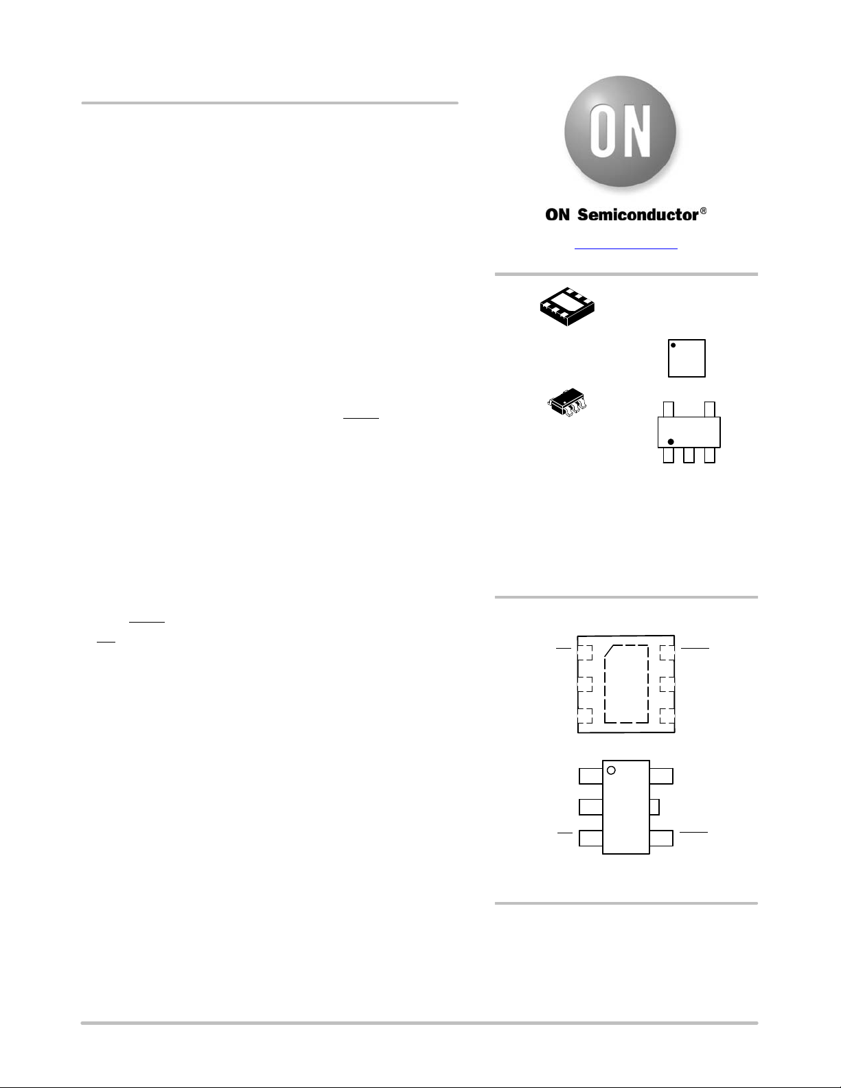
• UDFN6 2x2 mm and TSOP−5 3x3 mm Packages
• NCV Prefix for Automotive and Other Applications Requiring
Unique Site and Control Change Requirements; AEC−Q100
Qualified and PPAP Capable
• This is a Pb−Free Device
Applications
• USB Devices
• Mobile Phones
• Peripheral
• Personal Digital Applications
• MP3 Players
• Set Top Boxes
www.onsemi.com
MARKING
DIAGRAMS
6 PIN UDFN
CASE 517AB
5
1
TSOP−5
CASE 483
xxx = Specific Device Code
M = Date Code
A = Assembly Location
Y = Year
W = Work Week
G = Pb−Free Package
(Note: Microdot may be in either location)
PIN CONNECTIONS
1
GND
2
IN
3
UDFN
IN
1
GND
2
EN
3
TSOP−5
(Top View)
ORDERING INFORMATION
See detailed ordering and shipping information in the package
dimensions section on page 10 of this data sheet.
1
xxx AYWG
1
6
5
4
5
4
xx M
G
G
FLAGEN
OUT
OUT
OUT
FLAG
© Semiconductor Components Industries, LLC, 2012
February, 2019 − Rev. 5
1 Publication Order Number:
NCP361/D
NCP361, NCV361
INPUT
EN
1 mF 25 V X5R 0603
LDO V
INPUT
34
IN
C1
EN
OUT
OUT
NCP361
FLAG
GND
2
5
61
OUTPUT
1 mF 25 V X5R 0603
C2
FLAG
Figure 1. Typical Application Circuit (UDFN Pinout)
Thermal Shutdown
REF
Soft Start
UVLO
OVLO
FLAG Power
R1
1M
2
1
FLAG_State
J2
OUTPUT
(2 out pins in
UDFN package)
FLAGV
Figure 2. Functional Block Diagram
PIN FUNCTION DESCRIPTION (UDFN Package)
Pin No. Name Type Description
1 EN INPUT Enable Pin. The device enters in shutdown mode when this pin is tied to a high level. In this case the
2 GND POWER Ground
3 IN POWER Input Voltage Pin. This pin is connected to the VBUS. A 1 mF low ESR ceramic capacitor, or larger,
4, 5 OUT OUTPUT Output Voltage Pin. The output is disconnected from the VBUS power supply when the input voltage is
6 FLAG OUTPUT Fault Indication Pin. This pin allows an external system to detect a fault on VBUS pin. The FLAG pin
output is disconnected from the input. To allow normal functionality, the EN pin shall be connected to
GND or to a I/O pin. This pin does not have an impact on the fault detection.
must be connected between this pin and GND.
above OVLO threshold or below UVLO threshold. A 1 mF capacitor must be connected to these pins.
The two OUT pins must be hardwired to common supply.
goes low when input voltage exceeds OVLO threshold. Since the FLAG pin is open drain functionality,
an external pull up resistor to VCC must be added.
PIN FUNCTION DESCRIPTION (TSOP−5 Package)
Pin No. Name Type Description
1 IN POWER Input Voltage Pin. This pin is connected to the VBUS. A 1 mF low ESR ceramic capacitor, or larger,
2 GND POWER Ground
3 EN INPUT Enable Pin. The device enters in shutdown mode when this pin is tied to a high level. In this case the
4 FLAG OUTPUT Fault Indication Pin. This pin allows an external system to detect a fault on VBUS pin. The FLAG pin
5 OUT OUTPUT Output Voltage Pin. The output is disconnected from the VBUS power supply when the input voltage is
must be connected between this pin and GND.
output is disconnected from the input. To allow normal functionality, the EN pin shall be connected to
GND or to a I/O pin. This pin does not have an impact on the fault detection.
goes low when input voltage exceeds OVLO threshold. Since the FLAG pin is open drain functionality,
an external pull up resistor to VCC must be added.
above OVLO threshold or below UVLO threshold. A 1 mF capacitor must be connected to this pin.
NOTE: Pin out provided for concept purpose only and might change in the final product
www.onsemi.com
2
NCP361, NCV361
MAXIMUM RATINGS
Rating Symbol Value Unit
Minimum Voltage (IN to GND) Vmin
in
Minimum Voltage (All others to GND) Vmin −0.3 V
Maximum Voltage (IN to GND) Vmax
in
Maximum Voltage (All others to GND) Vmax 7.0 V
Maximum DC Current from Vin to Vout (PMOS) (Note 1) Imax 600 mA
Thermal Resistance, Junction−to−Air TSOP−5
R
q
JA
UDFN
Operating Ambient Temperature Range T
Storage Temperature Range T
Junction Operating Temperature T
ESD Withstand Voltage (IEC 61000−4−2)
A
stg
J
Vesd 15 Air, 8.0 Contact
Human Body Model (HBM), Model = 2 (Note 2)
Machine Model (MM) Model = B (Note 3)
Moisture Sensitivity MSL Level 1 −
Stresses exceeding those listed in the Maximum Ratings table may damage the device. If any of these limits are exceeded, device functionality
should not be assumed, damage may occur and reliability may be affected.
1. With minimum PCB area. By decreasing R
2. Human Body Model, 100 pF discharged through a 1.5 kW resistor following specification JESD22/A114.
, the current capability increases. See PCB recommendation page 9.
q
JA
3. Machine Model, 200 pF discharged through all pins following specification JESD22/A115.
−0.3 V
21 V
305
°C/W
240
−40 to +85 °C
−65 to +150 °C
150 °C
kV
2000
200
V
V
www.onsemi.com
3
NCP361, NCV361
ELECTRICAL CHARACTERISTICS
(Min/Max limits values (−40°C < T
Characteristic Symbol Conditions Min Typ Max Unit
Input Voltage Range V
Undervoltage Lockout Threshold UVLO Vin falls down UVLO threshold 2.85 3.0 3.15 V
Uvervoltage Lockout Hysteresis UVLO
Overvoltage Lockout Threshold OVLO Vin rises up OVLO threshold 5.43 5.675 5.9 V
Overvoltage Lockout Hysteresis OVLO
Vin versus V
Dopout V
out
Overcurrent Limit I
Supply Quiescent Current Idd No Load, Vin = 5.25 V 20 35 mA
Standby Current I
Zero Gate Voltage Drain Current
FLAG Output Low Voltage
FLAG Leakage Current
EN Voltage High V
EN Voltage Low V
EN Leakage Current
TIMINGS
Start Up Delay t
FLAG going up Delay
Output Turn Off Time t
Alert Delay t
Disable Time t
Thermal Shutdown Temperature T
Thermal Shutdown Hysteresis T
< +85°C) and Vin = +5.0 V. Typical values are TA = +25°C, unless otherwise noted.)
A
1.2 20 V
50 70 90 mV
50 100 125 mV
Vol
I
DSS
in
drop
lim
std
flag
hyst
hyst
Vin = 5 V, I charge = 500 mA 150 200 mV
Vin = 5 V 550 750 950 mA
Vin = 5 V, EN = 1.2 V 26 37 mA
VDS = 20 V, VGS = 0 V 0.08 mA
Vin > OVLO
Sink 1 mA on FLAG pin
FLAG
EN
t
start
on
off
leak
ih
il
leak
From Vin > UVLO to V
From Vin > UVLO to FLAG = 1.2 V, See Fig 3 & 10 3.0 ms
From Vin > OVLO to V
FLAG level = 5 V 5.0 nA
Vin from 3.3 V to 5.5 V 1.2 V
Vin from 3.3 V to 5.5 V 0.55 V
EN = 5.5 V or GND 170 nA
= 0.8xVin, See Fig 3 & 9 4.0 15 ms
out
≤ 0.3 V, See Fig 4 & 11
out
Vin increasing from 5 V to 8 V at 3 V/ms.
No output capacitor.
stop
From Vin > OVLO to FLAG ≤ 0.4 V, See Fig 4 & 12
Vin increasing from 5 V to 8 V at 3 V/ms
dis
From EN 0.4 to 1.2V to V
≤ 0.3 V, See Fig 5 & 13
out
Vin = 4.75 V.
No output capacitor.
sd
sdhyst
400 mV
0.7 1.5 ms
1.0 ms
3.0 ms
150 °C
30 °C
www.onsemi.com
4

NCP361, NCV361
<OVLO
x I
OVLO
t
off
t
stop
0.3 V
V
in
V
out
FLAG
UVLO
t
t
start
V
in
on
0.8 V
in
Vin − R
DS(on)
x I
1.2 V
Vin − R
V
out
FLAG
DSon
Figure 3. Start Up Sequence Figure 4. Shutdown on Over Voltage Detection
EN
V
out
Vin − R
DS(on)
1.2 V
x I
FLAG
Figure 5. Disable on EN
t
dis
0.3 V
= 1 Figure 6. FLAG Response with EN = 1
EN
V
out
FLAG
1.2 V
OVLO
UVLO
0.4 V
t
start
IN OUT
Voltage, Current and Thermal Detection
Figure 7.
IN OUT
Voltage, Current and Thermal Detection
Figure 8.
CONDITIONS
VIN > OVLO or VIN < UVLO
CONDITIONS
UVLO < VIN < OVLO
TYPICAL OPERATING CHARACTERISTICS
www.onsemi.com
5

NCP361, NCV361
Figure 9. Start Up. Vin=Ch1, Vout=Ch2 Figure 10. FLAG Going Up Delay. Vin=Ch1,
FL:AG=Ch3
Figure 11. Output Turn Off time. Vin=Ch1,
Vout=Ch2
Figure 13. Disable Time. EN=Ch4, Vin=Ch1,
Vout=Ch2
Figure 12. Alert Delay. Vout=Ch1, FLAG=Ch3
Figure 14. Thermal Shutdown. Vin=Ch1,
Vout=Ch2, FLAG=Ch3
www.onsemi.com
6

(mW)
DS(on)
R
450
400
350
300
250
200
150
100
50
0
NCP361, NCV361
TYPICAL OPERATING CHARACTERISTICS
Vin = 3.6 V
Vin = 5 V
0 50 100 150−50
TEMPERATURE (°C)
Figure 15. R
vs. Temperature
DS(on)
(Load = 500 mA)
180
160
140
120
100
80
60
40
20
SUPPLY QUIESCENT CURRENT (mA)
0
25°C
57911 171 3 13 15 19 21
125°C
−40°C
Vin, INPUT VOLTAGE (V)
Figure 17. Quiescent Current vs. Input Voltage
900
880
860
840
820
800
780
760
740
OVERCURRENT THRESHOLD (mA)
720
Figure 16. Output Short Circuit
900
880
860
840
820
800
780
760
740
OVERCURRENT THRESHOLD (mA)
720
050−50 100 150
Figure 18. Overcurrent Protection Threshold
25°C
85°C
3.5 43 4.5 5.5
INPUT VOLTAGE (V)
125°C
0°C
−25°C
−40°C
5
Vin = 3.25 V
Vin = 3.6 V
Vin = 4.2 V
Vin = 5 V
Vin = 5.25 V
TEMPERATURE (°C)
vs. Temperature
Figure 19. Overcurrent Protection Threshold
vs. Input Voltage
www.onsemi.com
7

NCP361, NCV361
Operation
NCP361 provides overvoltage protection for positive
voltage, up to 20 V. A PMOS FET protects the systems
(i.e.: VBUS) connected on the V
pin, against positive
out
overvoltage. The Output follows the VBUS level until
OVLO threshold is overtaken.
Undervoltage Lockout (UVLO)
To ensure proper operation under any conditions, the
device has a built−in undervoltage lock out (UVLO)
circuit. During Vin positive going slope, the output remains
disconnected from input until Vin voltage is above 3.0 V
nominal. The FLAGV output is pulled to low as long as V
does not reach UVLO threshold. This circuit has a 70 mV
hysteresis to provide noise immunity to transient condition.
Vin (V)
20 V
OVLO
UVLO
0
V
out
OVLO
UVLO
0
Figure 20. Output Characteristic vs. V
Overvoltage Lockout (OVLO)
To protect connected systems on V
in
pin from
out
overvoltage, the device has a built−in overvoltage lock out
(OVLO) circuit. During overvoltage condition (OVLO
exceeds), the output remains disabled and FLAG is tied
low, as long as the input voltage is higher than OVLO −
hysteresis. This circuit has a 100 mV hysteresis to provide
noise immunity to transient conditions.
Overcurrent Protection (OCP)
The NCP361 integrates overcurrent protection to
prevent system/battery overload or defect. The current
limit threshold is internally set at 750 mA. This value can
be changed from 150 mA to 750 mA by a metal tweak,
please contact your ON Semiconductor representative for
availability. During current fault, the internal PMOS FET
is automatically turned off (5 ms) if the charge current
exceeds I
. NCP361 goes into turn on and turn off mode
lim
as long as defect is present. The internal ton delay (4 ms
typical) allows limiting thermal dissipation. The Flag pin
goes to low level when an overcurrent fault appears. That
allows the microcontroller to count defect events and turns
off the PMOS with EN pin.
V
out
I
load
I
lim
in
Figure 21. Overcurrent Event Example
FLAG Output
Overload
t
on
Retrieve
normal
operation
NCP361 provides a FLAG output, which alerts external
systems that a fault has occurred.
This pin is tied to low as soon as: 1.2 V < Vin < UVLO,
Vin > OVLO, I
charge
> I
, TJ > 150°C. When NCP361
limit
recovers normal condition, FLAG is held high. The pin is
an open drain output, thus a pull up resistor (typically 1 MW
− Minimum 10 kW) must be provided to VCC. FLAG pin is
an open drain output.
EN Input
To enable normal operation, the EN pin shall be forced
to low or connected to ground. A high level on the pin
disconnects OUT pin from IN pin. EN does not overdrive
an OVLO or UVLO fault.
Internal PMOS FET
The NCP361 includes an internal PMOS FET to protect
the systems, connected on OUT pin, from positive
overvoltage. Regarding electrical characteristics, the
R
, during normal operation, will create low losses on
DS(on)
V
pin, characterized by Vin versus V
out
ESD Tests
dropout.
out
The NCP361 fully supports the IEC61000−4−2, level 4
(Input pin, 1 mF mounted on board). That means, in Air
condition, Vin has a ±15 kV ESD protected input. In
Contact condition, Vin has ±8 kV ESD protected input.
Please refer to Figure 22 to see the IEC61000−4−2
electrostatic discharge waveform.
www.onsemi.com
8

NCP361, NCV361
Figure 22.
PCB Recommendations
The NCP361 integrates a 500 mA rated PMOS FET, and
the PCB rules must be respected to properly evacuate the
heat out of the silicon. The UDFN PAD1 must be connected
to ground plane to increase the heat transfer if necessary
from an application standpoint. Of course, in any case, this
pad shall be not connected to any other potential.
By increasing PCB area, the R
of the package can be
JA
q
decreased, allowing higher charge current to fill the battery.
Taking into account that internal bondings (wires
between package and silicon) can handle up to 1 A (higher
than thermal capability), the following calculation shows
two different example of current capability, depending on
PCB area:
• With 305°C/W (without PCB area), allowing DC
current is 500 mA
• With 260°C/W (200 mm
allows with a 85°C ambient temperature is:
I = √(TJ-TA)/(R
I = 625 mA
In every case, we recommend to make thermal
measurement on final application board to make sure of the
final Thermal Resistance.
JA
q
2
), the charge DC current
x R
DSON
)
380
330
TSOP−5 1.0 oz
TSOP−5 2.0 oz
280
230
Theta JA (C/W)
180
130
80
0 100 200 300 400 500 600 700
Copper heat spreader area (mm^2)
DFN 2x2.2 1.0 oz
DFN 2x2.2 2.0 oz
% Delta DFN vs TSOP−5
50%
45%
40%
35%
30%
25%
20%
15%
10%
5%
0%
% Delta DFN vs TSOP−5
Figure 23. Thermal Resistance of UDFN 2x2 and TSOP Packages as a Function of PCB Area and Thickness
www.onsemi.com
9

NCP361, NCV361
ORDERING INFORMATION
Device Marking Package Shipping
NCP361MUTBG AD UDFN6
(Pb−Free)
NCP361SNT1G ACD TSOP−5
(Pb−Free)
NCV361SNT1G* VET TSOP−5
(Pb−Free)
†For information on tape and reel specifications, including part orientation and tape sizes, please refer to our Tape and Reel Packaging
Specifications Brochure, BRD8011/D.
*NCV Prefix for Automotive and Other Applications Requiring Unique Site and Control Change Requirements
3000 / Tape & Reel
3000 / Tape & Reel
3000 / Tape & Reel
SELECTION GUIDE
Part number is designated as follows:
NCP361xxxxxTxG
a
bc ed
Code Contents
a Overcurrent Threshold
b Package
c UVLO Typical Threshold
d OVLO Typical Threshold
e Tape & Reel Type
−: 750 mA
MU: UDFN
SN: TSOP−5
−: 3.00 V
−: 5.675 V
B: = 3000
1: = 3000
†
www.onsemi.com
10

MECHANICAL CASE OUTLINE
PACKAGE DIMENSIONS
5
1
SCALE 2:1
NOTE 5
2X
2X
T0.10
B
A
54
B
123
G
A
T0.20
TOP VIEW
0.05
H
SIDE VIEW
D
0.205XC AB
S
C
SEATING
C
PLANE
CASE 483
ISSUE N
K
J
END VIEW
TSOP−5
DETAIL Z
M
DETAIL Z
DATE 12 AUG 2020
NOTES:
1. DIMENSIONING AND TOLERANCING PER ASME
Y14.5M, 1994.
2. CONTROLLING DIMENSION: MILLIMETERS.
3. MAXIMUM LEAD THICKNESS INCLUDES LEAD FINISH
THICKNESS. MINIMUM LEAD THICKNESS IS THE
MINIMUM THICKNESS OF BASE MATERIAL.
4. DIMENSIONS A AND B DO NOT INCLUDE MOLD
FLASH, PROTRUSIONS, OR GATE BURRS. MOLD
FLASH, PROTRUSIONS, OR GATE BURRS SHALL NOT
EXCEED 0.15 PER SIDE. DIMENSION A.
5. OPTIONAL CONSTRUCTION: AN ADDITIONAL
TRIMMED LEAD IS ALLOWED IN THIS LOCATION.
TRIMMED LEAD NOT TO EXTEND MORE THAN 0.2
FROM BODY.
MILLIMETERS
DIM MIN MAX
A
2.85 3.15
B
1.35 1.65
C 0.90 1.10
D 0.25 0.50
G 0.95 BSC
H 0.01 0.10
J 0.10 0.26
K 0.20 0.60
M 0 10
__
S 2.50 3.00
SOLDERING FOOTPRINT*
1.9
0.95
0.037
1.0
0.039
*For additional information on our Pb−Free strategy and soldering
details, please download the ON Semiconductor Soldering and
Mounting Techniques Reference Manual, SOLDERRM/D.
0.074
0.028
0.7
2.4
0.094
SCALE 10:1
ǒ
inches
mm
GENERIC
MARKING DIAGRAM*
5
XXXAYWG
G
1
Analog
XXX = Specific Device Code
A = Assembly Location
Y = Year
W = Work Week
G = Pb−Free Package
(Note: Microdot may be in either location)
Ǔ
*This information is generic. Please refer to
device data sheet for actual part marking.
Pb−Free indicator, “G” or microdot “ G”,
may or may not be present.
5
XXX MG
G
1
Discrete/Logic
XXX = Specific Device Code
M = Date Code
G = Pb−Free Package
DOCUMENT NUMBER:
DESCRIPTION:
ON Semiconductor and are trademarks of Semiconductor Components Industries, LLC dba ON Semiconductor or its subsidiaries in the United States and/or other countries.
ON Semiconductor reserves the right to make changes without further notice to any products herein. ON Semiconductor makes no warranty, representation or guarantee regarding
the suitability of its products for any particular purpose, nor does ON Semiconductor assume any liability arising out of the application or use of any product or circuit, and specifically
disclaims any and all liability, including without limitation special, consequential or incidental damages. ON Semiconductor does not convey any license under its patent rights nor the
rights of others.
© Semiconductor Components Industries, LLC, 2018
98ARB18753C
TSOP−5
Electronic versions are uncontrolled except when accessed directly from the Document Repository.
Printed versions are uncontrolled except when stamped “CONTROLLED COPY” in red.
PAGE 1 OF 1
www.onsemi.com

MECHANICAL CASE OUTLINE
PACKAGE DIMENSIONS
SCALE 4:1
A B
E
A3
A
A1
L
3
C
SEATING
PLANE
L1
E2
4
6X
b
M
0.10 BC
M
0.05 C
6X
NOTE 4
PIN ONE
REFERENCE
0.10 C
0.10 C
0.10 C
0.08 C
DETAIL A
D
TOP VIEW
DETAIL B
SIDE VIEW
D2
1
6
e
BOTTOM VIEW
UDFN6 2x2, 0.65P
CASE 517AB
ISSUE C
NOTE 5
END VIEW
DETAIL A
ALTERNATE TERMINAL
CONSTRUCTIONS
A
MOLD CMPDEXPOSED Cu
DETAIL B
ALTERNATE
CONSTRUCTIONS
L
DATE 10 APR 2013
NOTES:
1. DIMENSIONING AND TOLERANCING PER ASME Y14.5M, 1994.
2. CONTROLLING DIMENSION: MILLIMETERS.
3. DIMENSION b APPLIES TO PLATED TERMINAL AND IS MEASURED
BETWEEN 0.15 AND 0.25MM FROM THE TERMINAL TIP.
4. COPLANARITY APPLIES TO THE EXPOSED PAD AS WELL AS THE
TERMINALS.
5. TIE BARS MAY BE VISIBLE IN THIS VIEW AND ARE CONNECTED TO
THE THERMAL PAD.
MILLIMETERS
DIMAMIN MAX
0.45 0.55
A1 0.00 0.05
A3 0.127 REF
b 0.25 0.35
D 2.00 BSC
A3
A1
D2 1.50 1.70
2.00 BSC
E
E2
0.80 1.00
e
0.65 BSC
0.25
L
L1
---
0.35
0.15
GENERIC
MARKING DIAGRAM*
XXMG
G
L
XX = Specific Device Code
M = Date Code
G = Pb−Free Package
(Note: Microdot may be in either location)
*This information is generic. Please refer to
device data sheet for actual part marking.
Pb−Free indicator, “G” or microdot “ G”,
may or may not be present.
RECOMMENDED
SOLDERING FOOTPRINT*
PACKAGE
OUTLINE
1.70
6X
0.47
0.95
2.30
1
0.65
PITCH
DIMENSIONS: MILLIMETERS
6X
0.40
*For additional information on our Pb−Free strategy and soldering
details, please download the ON Semiconductor Soldering and
Mounting Techniques Reference Manual, SOLDERRM/D.
DOCUMENT NUMBER:
DESCRIPTION:
ON Semiconductor and are trademarks of Semiconductor Components Industries, LLC dba ON Semiconductor or its subsidiaries in the United States and/or other countries.
ON Semiconductor reserves the right to make changes without further notice to any products herein. ON Semiconductor makes no warranty, representation or guarantee regarding
the suitability of its products for any particular purpose, nor does ON Semiconductor assume any liability arising out of the application or use of any product or circuit, and specifically
disclaims any and all liability, including without limitation special, consequential or incidental damages. ON Semiconductor does not convey any license under its patent rights nor the
rights of others.
© Semiconductor Components Industries, LLC, 2019
98AON22162D
UDFN6 2X2, 0.65P
Electronic versions are uncontrolled except when accessed directly from the Document Repository.
Printed versions are uncontrolled except when stamped “CONTROLLED COPY” in red.
PAGE 1 OF 1
www.onsemi.com

ON Semiconductor and are trademarks of Semiconductor Components Industries, LLC dba ON Semiconductor or its subsidiaries in the United States and/or other countries.
ON Semiconductor owns the rights to a number of patents, trademarks, copyrights, trade secrets, and other intellectual property. A listing of ON Semiconductor’s product/patent
coverage may be accessed at www.onsemi.com/site/pdf/Patent−Marking.pdf
ON Semiconductor makes no warranty, representation or guarantee regarding the suitability of its products for any particular purpose, nor does ON Semiconductor assume any liability
arising out of the application or use of any product or circuit, and specifically disclaims any and all liability, including without limitation special, consequential or incidental damages.
Buyer is responsible for its products and applications using ON Semiconductor products, including compliance with all laws, regulations and safety requirements or standards,
regardless of any support or applications information provided by ON Semiconductor. “Typical” parameters which may be provided in ON Semiconductor data sheets and/or
specifications can and do vary in different applications and actual performance may vary over time. All operating parameters, including “Typicals” must be validated for each customer
application by customer’s technical experts. ON Semiconductor does not convey any license under its patent rights nor the rights of others. ON Semiconductor products are not
designed, intended, or authorized for use as a critical component in life support systems or any FDA Class 3 medical devices or medical devices with a same or similar classification
in a foreign jurisdiction or any devices intended for implantation in the human body. Should Buyer purchase or use ON Semiconductor products for any such unintended or unauthorized
application, Buyer shall indemnify and hold ON Semiconductor and its officers, employees, subsidiaries, affiliates, and distributors harmless against all claims, costs, damages, and
expenses, and reasonable attorney fees arising out of, directly or indirectly, any claim of personal injury or death associated with such unintended or unauthorized use, even if such
claim alleges that ON Semiconductor was negligent regarding the design or manufacture of the part. ON Semiconductor is an Equal Opportunity/Affirmative Action Employer. This
literature is subject to all applicable copyright laws and is not for resale in any manner.
. ON Semiconductor reserves the right to make changes without further notice to any products herein.
PUBLICATION ORDERING INFORMATION
LITERATURE FULFILLMENT:
Email Requests to: orderlit@onsemi.com
ON Semiconductor Website: www.onsemi.com
TECHNICAL SUPPORT
North American Technical Support:
Voice Mail: 1 800−282−9855 Toll Free USA/Canada
Phone: 011 421 33 790 2910
Europe, Middle East and Africa Technical Support:
Phone: 00421 33 790 2910
For additional information, please contact your local Sales Representative
◊
www.onsemi.com
1
 Loading...