


Buck Converter - DC-DC,
High Efficiency, Adjustable
Output Voltage, Low Ripple
1.7 MHz, 1 A
NCP1529
The NCP1529 step−down DC−DC converter is a monolithic
integrated circuit for portable applications powered from one cell
Li−ion or three cell Alkaline/NiCd/NiMH batteries. The device is able
to deliver up to 1.0 A on an output voltage range externally adjustable
from 0.9 V to 3.9 V or fixed at 1.2 V or 1.35 V. It uses synchronous
rectification to increase efficiency and reduce external part count. The
device also has a built−in 1.7 MHz (nominal) oscillator which reduces
component size by allowing a small inductor and capacitors. Automatic
switching PWM/PFM mode offers improved system efficiency.
Additional features include integrated soft−start, cycle−by−cycle
current limiting and thermal shutdown protection.
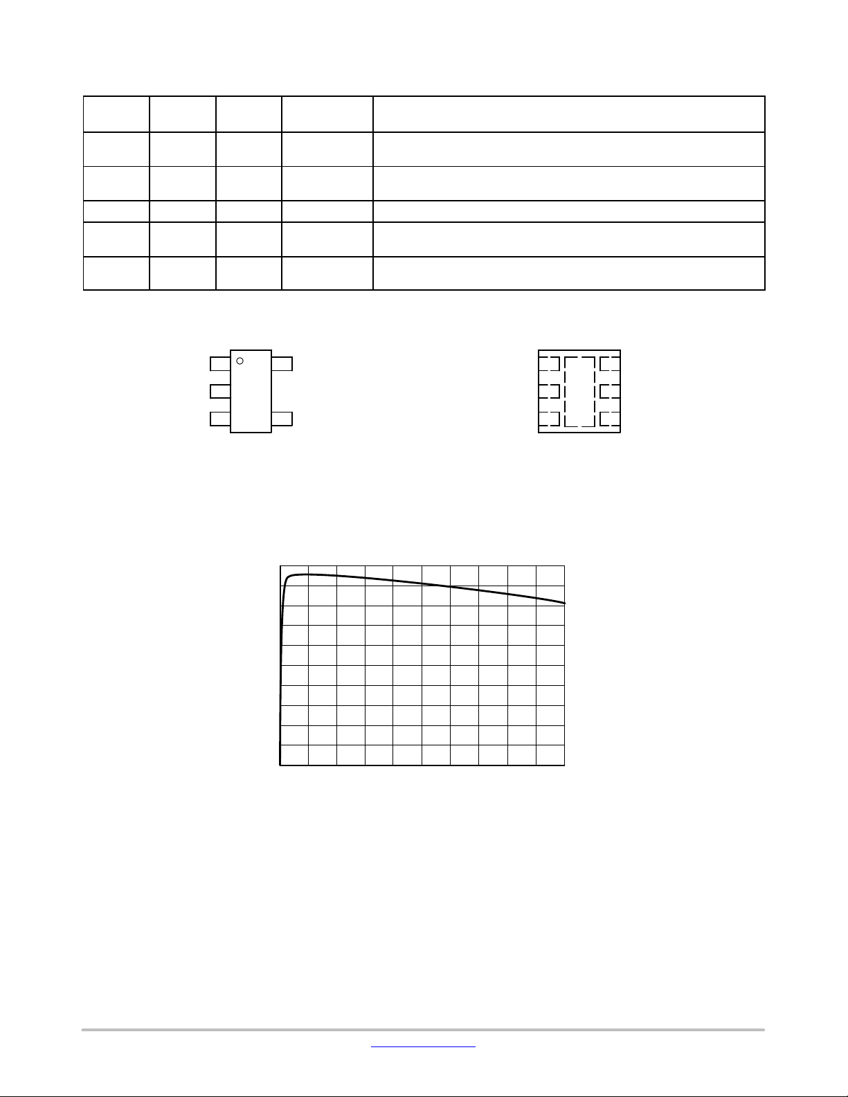
The NCP1529 is available in a space saving, low profile
2x2x0.5 mm UDFN6 package and TSOP−5 package.
Features
• Up to 96% Efficiency
• Best In Class Ripple, including PFM mode
• Source up 1.0 A
• 1.7 MHz Switching Frequency
• Adjustable from 0.9 V to 3.9 V or Fixed at 1.2 V or 1.35 V
• Synchronous rectification for higher efficiency
• 2.7 V to 5.5 V Input Voltage Range
• Low Quiescent Current 28 mA
• Shutdown Current Consumption of 0.3 mA
• Thermal Limit Protection
• Short Circuit Protection
• All Pins are Fully ESD Protected
• These are Pb−Free Devices
Typical Applications
• Cellular Phones, Smart Phones and PDAs
• Digital Still Cameras
• MP3 Players and Portable Audio Systems
• Wireless and DSL Modems
• USB Powered Devices
• Portable Equipment
V
IN
OFF ON
VINENSW
C
IN
FB
GND
L
C
OUT
R1
R2
V
OUT
C
ff
OFF ON
www.onsemi.com
MARKING
DIAGRAM
5
TSOP−5
5
1
DXJ = Specific Device Code
A = Assembly Location
Y = Year
W = Work Week
G = Pb−Free Package
(Note: Microdot may be in either location)
XX = Specific Device Code
M = Date Code
G = Pb−Free Package
(Note: Microdot may be in either location)
ORDERING INFORMATION
See detailed ordering and shipping information in the package
dimensions section on page 14 of this data sheet.
V
IN
C
IN
SN SUFFIX
CASE 483
UDFN6
MU SUFFIX
CASE 517AB
VINENSW
FB
GND
1
1
2
3
L
DXJAYWG
G
XXMG
G
V
OUT
C
OUT
6
5
4
Figure 1. Typical Application for Adjustable Version
© Semiconductor Components Industries, LLC, 2010
August, 2020− Rev. 6
Figure 2. Typical Application for Fixed Version
1 Publication Order Number:
NCP1529/D
NCP1529
PIN FUNCTION DESCRIPTION
Pin
TSOP−5
1 6 EN Analog Input Enable for switching regulators. This pin is active HIGH and is turned off by
2 2,4,7
3 5 SW Analog Output Connection from power MOSFETs to the Inductor.
4 3 VIN Analog /
5 1 FB Analog Input Feedback voltage from the output of the power supply. This is the input to the
1. Exposed pad for UDFN6 package, named Pin 7, must be connected to system ground.
Pin
UDFN6
(Note 1)
Pin Name Type Description
logic LOW on this pin.
GND Analog /
Power Ground
Power Input
This pin is the GND reference for the NFET power stage and the analog
section of the IC. The pin must be connected to the system ground.
Power supply input for the PFET power stage, analog and digital blocks. The
pin must be decoupled to ground by a 4.7 mF ceramic capacitor.
error amplifier.
PIN CONNECTIONS
EN
GND
SW
1
2
3
(Top View)
FB
5
4
VIN
FB
GND
VIN
1
2
3
(Top View)
7
EN
6
5
SW
4
GND
Figure 3. Pin Connections − TSOP−5 Figure 4. Pin Connections − UDFN6
PERFORMANCES
100
90
80
70
60
50
40
30
EFFICIENCY (%)
20
10
0
0 500 1000
I
(mA)
OUT
Figure 5. Efficiency vs Output Current
V
= 3.6 V, V
IN
OUT
= 3.3 V
www.onsemi.com
2
NCP1529
FUNCTIONAL BLOCK DIAGRAM
Q1
V
4.7 mF
Enable
battery
VIN
GND
EN
LOGIC
CONTROL
& THERMAL
SHUTDOWN
Q2
PWM/PFM
CONTROL
I
LIMIT
REFERENCE
VOLTAGE
Figure 6. Simplified Block Diagram
SW
FB
2.2 mH
10 mF
R1
R2
18 pF
www.onsemi.com
3
NCP1529
MAXIMUM RATINGS
Rating Symbol Value Unit
Minimum Voltage All Pins V
Maximum Voltage All Pins (Note 2) V
Maximum Voltage EN V
Thermal Resistance, Junction−to−Air (TSOP−5 Package)
Thermal Resistance using TSOP−5 Recommended Board Layout (Note 9)
Thermal Resistance, Junction−to−Air (UDFN6 Package)
Thermal Resistance using UDFN6 Recommended Board Layout (Note 9)
Operating Ambient Temperature Range (Notes 7 and 8) T
Storage Temperature Range T
Junction Operating Temperature (Notes 7 and 8) T
min
max
max
R
q
JA
R
q
JA
A
stg
j
Latchup Current Maximum Rating (TA = 85°C) (Note 5) Other Pins Lu $100 mA
ESD Withstand Voltage (Note 4)
Human Body Model
V
esd
Machine Model
Moisture Sensitivity Level (Note 6) MSL 1 per IPC
Stresses exceeding those listed in the Maximum Ratings table may damage the device. If any of these limits are exceeded, device functionality
should not be assumed, damage may occur and reliability may be affected.
2. Maximum electrical ratings are defined as those values beyond which damage to the device may occur at T
3. According to JEDEC standard JESD22−A108B.
4. This device series contains ESD protection and exceeds the following tests:
Human Body Model (HBM) per JEDEC standard: JESD22−A114.
Machine Model (MM) per JEDEC standard: JESD22−A115.
5. Latchup current maximum rating per JEDEC standard: JESD78.
6. JEDEC Standard: J−STD−020A.
7. In applications with high power dissipation (low V
considerations − thermal dissipation vias, traces or planes and PCB material − can significantly improve junction to air thermal resistance
(for more information, see design and layout consideration section). Environmental conditions such as ambient temperature TA brings
R
q
JA
thermal limitation on maximum power dissipation allowed.
, high I
IN
), special care must be paid to thermal dissipation issues. Board design
OUT
The following formula gives calculation of maximum ambient temperature allowed by the application:
= TJ
T
A MAX
Where: T
8. To prevent permanent thermal damages, this device include a thermal shutdown which engages at 180°C (typ).
− (R
x Pd)
MAX
is the junction temperature,
J
is the maximum power dissipated by the device (worst case of the application),
P
d
and R
q
JA
is the junction−to−ambient thermal resistance.
q
JA
9. Board recommended TSOP−5 and UDFN6 layouts are described on Layout Considerations section.
−0.3 V
7.0 V
VIN + 0.3 V
300
°C/W
110
220
°C/W
40
−40 to 85 °C
−55 to 150 °C
−40 to 150 °C
2.0
kV
200
= 25°C.
A
V
1200
1000
800
UDFN6
TSOP−5
600
400
, POWER DISSIPATION (mW)
200
D
P
0
−40 −200 20 406080
TA, AMBIENT TEMPERATURE (°C)
Figure 8. Power Derating
www.onsemi.com
1200
UDFN6
1000
800
TSOP−5
600
RENT (mA)
400
, MAXIMUM OUTPUT CUR-
200
OUTmax
I
0
2.7 3.2 3.7 4.2 4.7 5.2
, INPUT VOLTAGE (V)
V
IN
Figure 7. Maximum Output Current, TA = 455C
4
NCP1529
ELECTRICAL CHARACTERISTICS (Typical values are referenced to T
+85°C ambient temperature, unless otherwise noted, operating conditions V
= +25°C, Min and Max values are referenced −40°C to
A
= 3.6 V, V
IN
= 1.2 V, unless otherwise noted.)
OUT
Rating Conditions Symbol Min Typ Max Unit
INPUT VOLTAGE
Input Voltage Range
Quiescent Current No Switching, No load I
Standby Current EN Low I
Under Voltage Lockout VIN Falling V
Under Voltage Hysteretis V
V
in
Q
STB
UVLO
UVLOH
2.7 − 5.5 V
− 28 39
− 0.3 1.0
mA
mA
2.2 2.4 2.55 V
− 100 − mV
ANALOG AND DIGITAL PIN
Positive going Input High Voltage Threshold
Negative going Input High Voltage Threshold V
EN Threshold Hysteresis V
EN High Input Current EN = 3.6 V I
V
IH
ENH
ENH
1.2 − − V
− − 0.4 V
IL
− 100 − mV
− 1.5 −
mA
OUTPUT
Feedback Voltage Level
Output Voltage Range (Notes 10, 11)
Adjustable Version
Fixed Version at 1.2 V
Fixed Version at 1.35 V
USB or 5 V Rail Powered Applications
V
V
OUT
FB
−
0.6
−
1.2
−
1.35
0.9
0.9−−
3.3
3.9
−
V
−
−
V
(VIN from 4.3 V to 5.5 V) (Note 12)
Output Voltage Accuracy Room Temperature (Note 13)
Overtemperature Range
Maximum Output Current (Note 10) I
Output Voltage Load Regulation
Overtemperature
Load Transient Response
Rise/Fall Time 1 ms
Load = 100 mA to 1000 mA (PWM Mode)
Load = 0 mA to 100 mA (PFM Mode)
10 mA to 100 mA Load Step
(PFM to PWM Mode)
200 mA to 600 mA Load Step
DV
OUT
OUTMAX
V
LOADR
V
LOADT
−−3$1$2−
+3
1 − − A
−−−0.9
1.1−−
−−40
85
−
mV
−
%
%
(PWM to PWM Mode)
Output Voltage Line Regulation Load = 100 mA VIN = 2.7 V to 5.5 V V
Line Transient Response Load = 100 mA
Output Voltage Ripple I
3.6 V to 3.2 V Line Step (Fall Time = 50 ms)
= 0 mA
OUT
I
= 300 mA
OUT
V
V
Switching Frequency F
LINER
LINET
RIPPLE
SW
− 0.05 − %
− 6.0 − mV
−−8.0
mV
3.0−−
1.2 1.7 2.2 MHz
PP
PP
Duty Cycle D − − 100 %
Soft−Start Time Time from EN to 90% of Output Voltage t
START
− 310 500
ms
POWER SWITCHES
High−Side MOSFET On−Resistance
Low−Side MOSFET On−Resistance R
High−Side MOSFET Leakage Current I
Low−Side MOSFET Leakage Current I
R
ONHS
ONLS
LEAKHS
LEAKLS
− 400 −
− 300 −
− 0.05 −
− 0.01 −
mW
mW
mA
mA
PROTECTION
DC−DC Short Circuit Protection
Thermal Shutdown Threshold T
Thermal Shutdown Hysteresis T
Peak Inductor Current I
PK
SD
SDH
− 1.6 − A
− 180 − °C
− 40 − °C
10.Functionality guaranteed per design and characterization.
11.Whole output voltage range is available for adjustable versions only. By topology, the maximum output voltage will be equal or lower than
the input voltage.
12.See chapter ”USB or 5 V Rail Powered Applications”.
13. For adjustable versions only, the overall output voltage tolerance depends upon the accuracy of the external resistor (R1 and R2). Specified
value assumes that external resistor have 0.1% tolerance.
www.onsemi.com
5

NCP1529
TABLE OF GRAPHS
Typical Characteristics for Step−down Converter Figure
h
I
q ON
I
q OFF
F
SW
V
LOADR
V
LOADT
V
LINER
V
LINET
t
START
I
PK
V
UVLO
VIL, V
P, G Phase & Gain Performance 24
Efficiency vs. Output Current 10, 11, 12
Quiescent Current, PFM no load vs. Input Voltage 9
Standby Current, EN Low vs. Input Voltage 8
Switching Frequency vs. Ambient Temperature 13
Load Regulation vs. Load Current 14
Load Transient Response 16, 17
Line Regulation vs. Output Current 15
Line Transient Response 18, 19
Soft Start 20
Short Circuit Protection 21
Under Voltage Lockout Threshold vs. Ambient Temperature 22
Enable Threshold vs. Ambient Temperature 23
IH
www.onsemi.com
6
 Loading...