

NCP1271
PW
M Controller, Soft-Skip &
trade; Standby, with
Adjustable Skip Level and
External Latch
The NCP1271 represents a new, pin to pin compatible, generation
of the successful 7−pin current mode NCP12XX product series. The
controller allows for excellent stand by power consumption by use of
its adjustable Soft−Skip mode and integrated high voltage startup
FET. This proprietary Soft−Skip also dramatically reduces the risk of
acoustic noise. This allows the use of inexpensive transformers and
capacitors in the clamping network. Internal frequency jittering, ramp
compensation, timer−based fault detection and a latch input make
this controller an excellent candidate for converters where
ruggedness and component cost are the key constraints.
Features
• Fixed−Frequency Current−Mode Operation with Ramp
Compensation and Skip Cycle in Standby Condition
• Timer−Based Fault Protection for Improved Overload Detection
• “Soft−Skip Mode” Technique for Optimal Noise Control in Standby
• Internal High−Voltage Startup Current Source for Lossless Startup
• "5% Current Limit Accuracy over the Full Temperature Range
• Adjustable Skip Level
• Internal Latch for Easy Implementation of Overvoltage and
Overtemperature Protection
• Frequency Jittering for Softened EMI Signature
• +500 mA/−800 mA Peak Current Drive Capability
• Sub−100 mW Standby Power can be Achieved
• Pin−to−Pin Compatible with the Existing NCP120X Series
• This is a Pb−Free Device
Typical Applications
• AC−DC Adapters for Notebooks, LCD Monitors
• Offline Battery Chargers
• Consumer Electronic Appliances STB, DVD, DVDR
http://onsemi.com
SOIC−7
D SUFFIX
CASE 751U
PDIP−7 VHVIC
P SUFFIX
CASE 626B
8
1
x = A or B
A= 65 kHz
B= 100 kHz
xxx = Device Code: 65, 100
A = Assembly Location
L, WL = Wafer Lot
Y, YY = Year
W, WW = Work Week
G or G = Pb−Free Package
(Note: Microdot may be in either location)
PIN CONNECTIONS
FB
CS
GND
1
2
3
4
(Top View)
Skip/latch
1
8
6
5
MARKING
DIAGRAMS
8
1271x
ALYWG
G
1
1271Pxxx
AWL
YYWWG
HV
V
CC
Drv
*For additional information on our Pb−Free strategy and soldering details, please
download the ON Semiconductor Soldering and Mounting Techniques Reference
Manual, SOLDERRM/D.
© Semiconductor Components Industries, LLC, 2009
September, 2009 − Rev. 6
1 Publication Order Number:
ORDERING INFORMATION
See detailed ordering and shipping information in the package
dimensions section on page 19 of this data sheet.
NCP1271/D
NCP1271
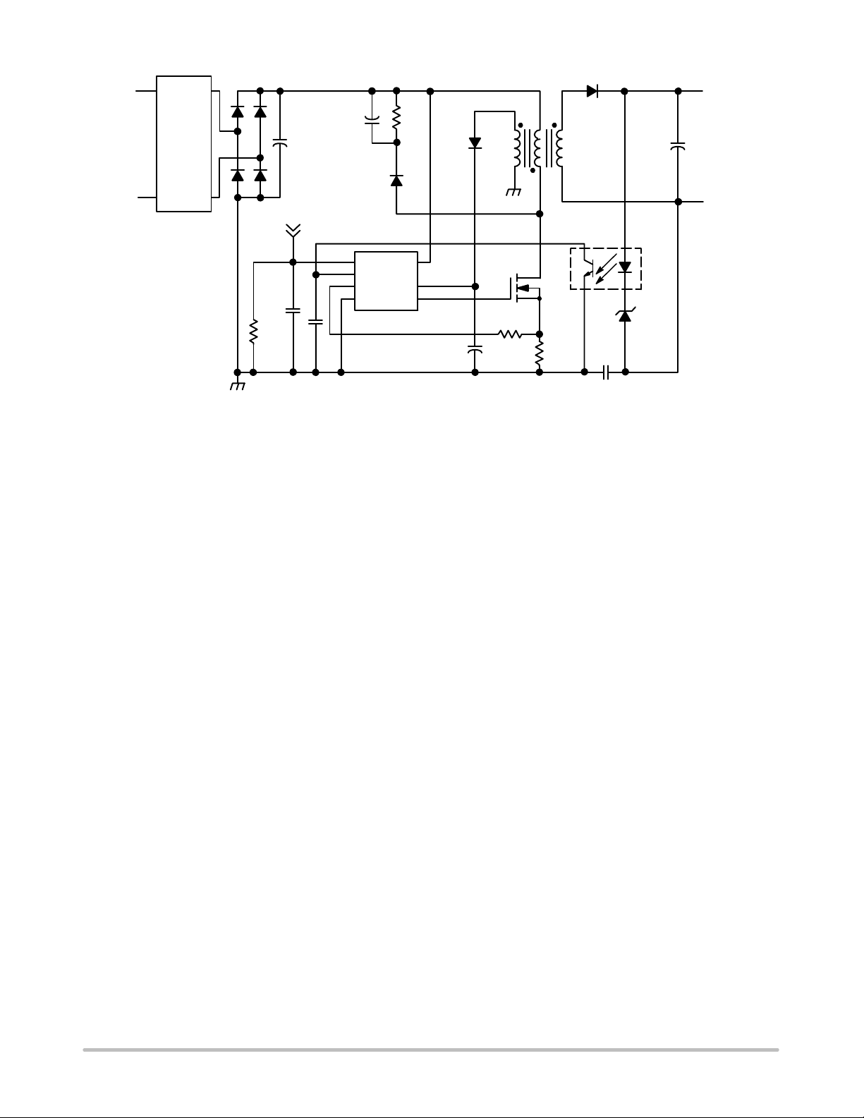
+
AC
Input
*Optional
EMI
Filter
R
skip
latch input*
skip/latch
FB
CS
Gnd
HV
Vcc
Drv
NCP1271
Figure 1. Typical Application Circuit
R
*
ramp
Output
Voltage
−
http://onsemi.com
2

NCP1271
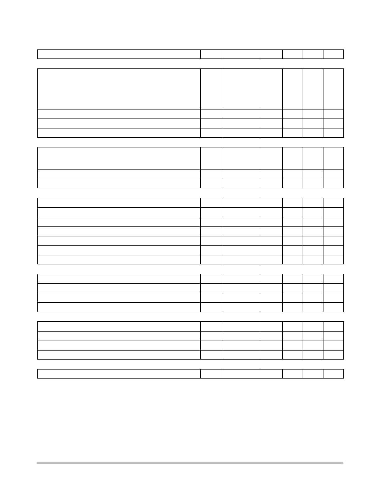
MAXIMUM RATINGS (Notes 1 and 2)
Rating Symbol Value Unit
VCC Pin (Pin 6)
Maximum Voltage Range
Maximum Current
Skip/Latch, FB, CS Pin (Pins 1−3)
Maximum Voltage Range
Maximum Current
Drv Pin (Pin 5)
Maximum Voltage Range
Maximum Current
HV Pin (Pin 8)
Maximum Voltage Range
Maximum Current
Power Dissipation and Thermal Characteristics
Thermal Resistance, Junction−to−Air, PDIP−7, Low Conductivity PCB (Note 3)
Thermal Resistance, Junction−to−Lead, PDIP−7, Low Conductivity PCB
Thermal Resistance, Junction−to−Air, PDIP−7, High Conductivity PCB (Note 4)
Thermal Resistance, Junction−to−Lead, PDIP−7, High Conductivity PCB
Thermal Resistance, Junction−to−Air, SO−7, Low Conductivity PCB (Note 3)
Thermal Resistance, Junction−to−Lead, SO−7, Low Conductivity PCB
Thermal Resistance, Junction−to−Air, SO−7, High Conductivity PCB (Note 4)
Thermal Resistance, Junction−to−Lead, SO−7, High Conductivity PCB
Operating Junction Temperature Range T
Maximum Storage Temperature Range T
ESD Protection
Human Body Model ESD Pins 1−6
Human Body Model ESD Pin 8
Machine Model ESD Pins 1−4, 8
Machine Model ESD Pins 5, 6
Charged Device Model ESD
Stresses exceeding Maximum Ratings may damage the device. Maximum Ratings are stress ratings only. Functional operation above the
Recommended Operating Conditions is not implied. Extended exposure to stresses above the Recommended Operating Conditions may affect
device reliability.
1. ESD protection per JEDEC JESD22−A114−F for HBM, per JEDEC JESD22−A115−A for MM, and per JEDEC JESD22−C101D for CDM.
This device contains latchup protection and exceeds 100 mA per JEDEC Standard JESD78.
2. Guaranteed by design, not tested.
3. As mounted on a 40x40x1.5 mm FR4 substrate with a single layer of 80 mm2 of 2 oz copper traces and heat spreading area. As specified for
a JEDEC 51 low conductivity test PCB. Test conditions were under natural convection or zero air flow.
4. As mounted on a 40x40x1.5 mm FR4 substrate with a single layer of 650 mm2 of 2 oz copper traces and heat spreading area. As specified
for a JEDEC 51 high conductivity test PCB. Test conditions were under natural convection or zero air flow.
V
max
I
max
V
max
I
max
V
max
I
max
V
max
I
max
R
q
JA
R
q
JL
R
q
JA
R
q
JL
R
q
JA
R
q
JL
R
q
JA
R
q
JL
J
stg
HBM
HBM
MM
MM
CDM
−0.3 to +20
100
−0.3 to +10
100
−0.3 to +20
−800 to +500
−0.3 to +500
100
142
57
120
56
177
75
136
69
°C/W
°C/W
°C/W
°C/W
°C/W
°C/W
°C/W
°C/W
−40 to +150 °C
−60 to +150 °C
2000
700
200
150
1000
V
mA
V
mA
V
mA
V
mA
V
V
V
V
V
http://onsemi.com
3
NCP1271
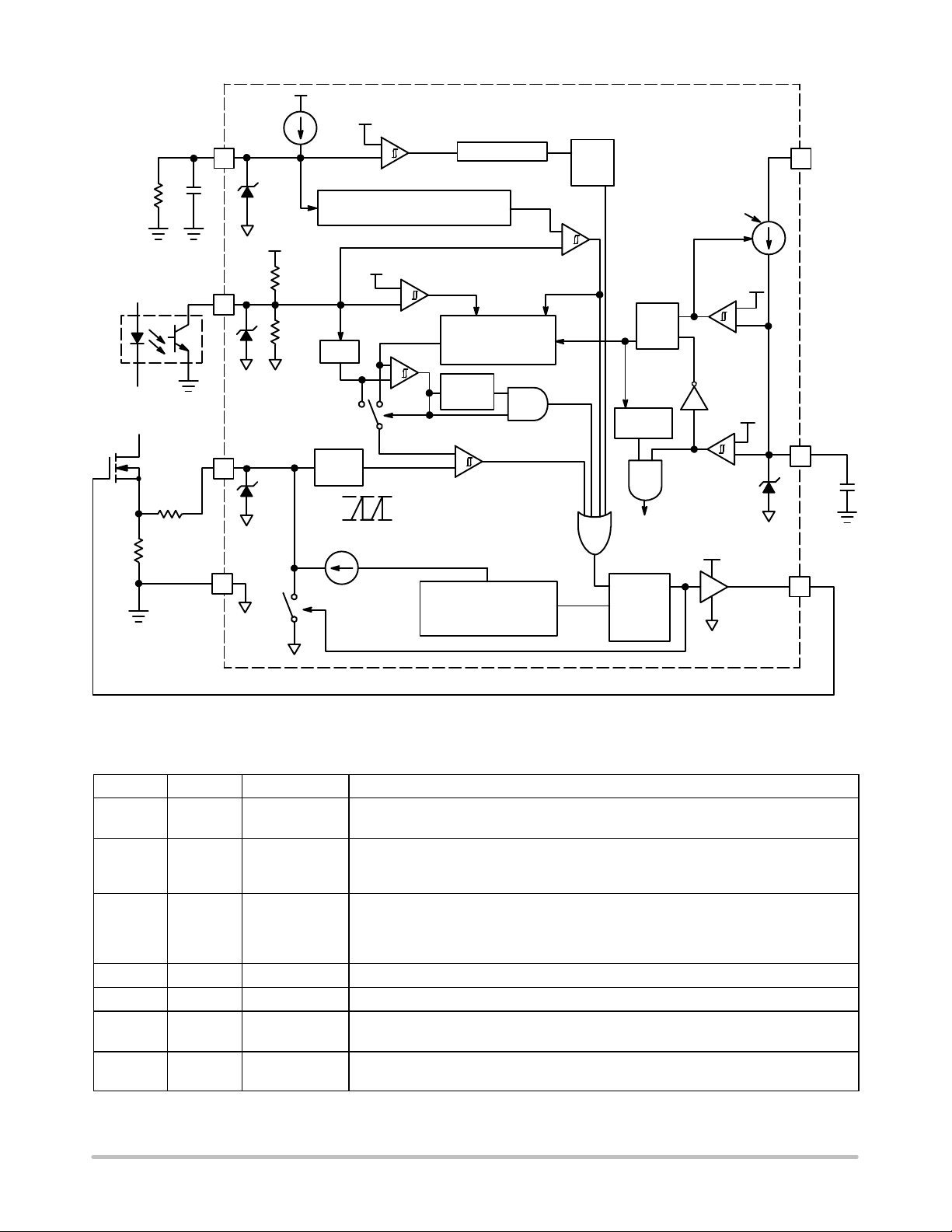
R
skip
Skip/ latch
R
ramp
R
CS
FB
CS
Gnd
I
skip
1
−
+
13 us filter
S
R
10V
V
= R
* I
skip
skip
or
skip
= 1.2 V when pin 1 is opened
V
skip
4.8 V
2.85 V
FB
16.7k
V
2
75.3k
1 / 3
10V
V
3
CS
V / 3
FB
0
180 ns
LEB
10V
TLD
−
+
V
ss
(1V max)
−
+
1
V
PWM
100uA
Soft start/ soft−skip
management
4 ms/ 300 us
130ms
delay
PWM
−
+
disable
soft
skip
V
V
skip
FB
&
skip
+
−
soft−skip
soft
start
short
circuit
fault
0
jittered ramp
current source
latch−off, reset
when Vcc < 4V
Q
4.1 mA when Vcc > 0.6 V
0.2 mA when Vcc < 0.6 V
S
Q
R
double
hiccup
B2
Counter
&
turn on internal bias
OR
turn off
V
−
+
UVLO
−
+
CC
12.6/
5.8 V
9.1 V
20V
8
HV
V
CC
6
Drv
8 V
4
1 0
7.5% Jittering
65, 100 kHz
Oscillator
R
S
Max duty
= 80%
Q
driver:
+500 mA
/ −800 mA
5
Figure 2. Functional Block Diagram
PIN FUNCTION DESCRIPTION
Pin No. Symbol Function Description
1 Skip/latch Skip Adjust or
Latchoff
A resistor to ground provides the adjustable standby skip level. Additionally, if this pin is
pulled higher than 8.0 V (typical), the controller latches off the drive.
2 FB Feedback An optocoupler collector pulls this pin low during regulation. If this voltage is less than
the Skip pin voltage, then the driver is pulled low and Soft−Skip mode is activated. If this
pin is open (>3 V) for more than 130 ms, then the controller is placed in a fault mode.
3 CS Current Sense This pin senses the primary current for PWM regulation. The maximum primary current
is limited to 1.0 V / RCS where RCS is the current sense resistor. Additionally, a ramp
resistor R
between the current sense node and this pin sets the compensation ramp
ramp
for improved stability.
4 Gnd IC Ground −
5 Drv Driver Output The NCP1271’s powerful output is capable of driving the gates of large Qg MOSFETs.
6 V
CC
Supply Voltage This is the positive supply of the device. The operating range is between 10 V (min) and
20 V (max) with a UVLO start threshold 12.6 V (typ).
8 HV High Voltage This pin provides (1) Lossless startup sequence (2) Double hiccup fault mode (3)
Memory for latch−off shutdown and (4) Device protection if VCC is shorted to GND.
http://onsemi.com
4
NCP1271
ELECTRICAL CHARACTERISTICS (For typical values T
= 25°C, for min/max values, TJ = −40°C to +125°C, VCC = 14 V,
J
HV = open, skip = open, FB = 2 V, CS = Ground, DRV = 1 nF, unless otherwise noted.)
Characteristic Pin Symbol Min Typ Max Unit
OSCILLATOR
Oscillation Frequency (65 kHz Version, T
= 25_C)
J
Oscillation Frequency (65 kHz Version, TJ = −40 to + 85_C)
Oscillation Frequency (65 kHz Version, T
Oscillation Frequency (100 kHz Version, T
= −40 to + 125_C)
J
= 25_C)
J
Oscillation Frequency (100 kHz Version, TJ = −40 to +85_C)
Oscillation Frequency (100 kHz Version, TJ = −40 to +125_C)
Oscillator Modulation Swing, in Percentage of f
osc
5 f
osc
61.75
58
55
95
89
85
65
65
65
100
100
100
68.25
69
69
105
107
107
5 − − "7.5 − %
Oscillator Modulation Swing Period 5 − − 6.0 − ms
Maximum Duty Cycle (VCS = 0 V, VFB = 2.0 V) 5 D
max
75 80 85 %
GATE DRIVE
Gate Drive Resistance
Output High (V
= 14 V, Drv = 300 W to Gnd)
CC
Output Low (VCC = 14 V, Drv = 1.0 V)
Rise Time from 10% to 90% (Drv = 1.0 nF to Gnd) 5 t
Fall Time from 90% to 10% (Drv = 1.0 nF to Gnd) 5 t
5
R
OH
R
OL
r
f
6.0
2.0
11
6.0
20
12
− 30 − ns
− 20 − ns
CURRENT SENSE
Maximum Current Threshold 3 I
Soft−Start Duration − t
Soft−Skip Duration − t
Leading Edge Blanking Duration 3 t
Limit
SS
SK
LEB
0.95 1.0 1.05 V
− 4.0 − ms
− 300 − ms
100 180 330 ns
Propagation Delay (Drv =1.0 nF to Gnd) − − − 50 150 ns
Ramp Current Source Peak 3 I
Ramp Current Source Valley 3 I
ramp(H)
ramp(L)
− 100 − mA
− 0 − mA
SKIP
Default Standby Skip Threshold (Pin 1 = Open) 2 V
Skip Current (Pin 1 = 0 V, TJ = 25_C) 1 I
Skip Level Reset (Note 5) 1 V
skip−reset
Transient Load Detection Level to Disable Soft−Skip Mode 2 V
skip
skip
TLD
− 1.2 − V
26 43 56 mA
5.0 5.7 6.5 V
2.6 2.85 3.15 V
EXTERNAL LATCH
Latch Protection Threshold 1 V
Latch Threshold Margin (V
latch−m
= V
CC(off)
− V
) 1 V
latch
latch
latch−m
7.1 8.0 8.7 V
0.6 1.2 − V
Noise Filtering Duration 1 − − 13 − ms
Propagation Delay (Drv = 1.0 nF to Gnd) 1 T
latch
− 100 − ns
SHORT−CIRCUIT FAULT PROTECTION
Time for Validating Short−Circuit Fault Condition 2 t
protect
− 130 − ms
5. Please refer to Figure 39 for detailed description.
6. Guaranteed by design.
kHz
W
http://onsemi.com
5
NCP1271
ELECTRICAL CHARACTERISTICS (continued) (For typical values T
= 25°C, for min/max values, TJ = −40°C to +125°C,
J
VCC = 14 V, HV = open, skip = open, FB = 2 V, CS = Ground, DRV = 1 nF, unless otherwise noted.)
Characteristic Pin Symbol Min Typ Max Unit
STARTUP CURRENT SOURCE
High−Voltage Current Source
Inhibit Voltage (I
Inhibit Current (V
Startup (V
= 200 mA, HV = 50 V)
CC
= 0 V, HV = 50 V)
CC
= V
CC
CC(on)
− 0.2 V, HV = 50 V)
Leakage (VCC = 14 V, HV = 500 V)
Minimum Startup Voltage (VCC = V
– 0.2 V, ICC = 0.5 mA) 8 V
CC(on)
6
6
6
8
V
inhibit
I
inhibit
I
HV
I
HV−leak
HV(min)
SUPPLY SECTION
VCC Regulation
Startup Threshold, VCC Increasing
Minimum Operating Voltage After Turn−On
V
Operating Hysteresis
CC
Undervoltage Lockout Threshold Voltage, V
Logic Reset Level (V
CC(latc h)
–V
CC(reset)
Decreasing
CC
> 1.0 V) (Note 7)
VCC Supply Current
Operating (VCC = 14 V, 1.0 nF Load, VFB = 2.0 V, 65 kHz Version)
Operating (VCC = 14 V, 1.0 nF Load, VFB = 2.0 V, 100 kHz Version)
Output Stays Low (VCC = 14 V, VFB = 0 V)
Latchoff Phase (VCC = 7.0 V, VFB = 2.0 V)
6
V
CC(on)
V
CC(off)
V
− V
CC(on)
V
CC(latc h)
V
CC(reset)
6
I
CC1
I
CC1
I
CC2
I
CC3
7. Guaranteed by design.
CC(off)
190
80
3.0
10
600
200
4.1
25
800
350
6.0
50
− 20 28 V
11.2
8.2
3.0
5.0
12.6
9.1
3.6
5.8
−
−
−
−
−
4.0
2.3
3.1
1.3
500
13.8
10
4.2
6.5
−
3.0
3.5
2.0
720
mV
mA
mA
mA
V
V
V
V
V
mA
mA
mA
mA
110
100
90
80
70
60
OSCILLATION FREQUENCY (kHz)
50
−25 −25
Figure 3. Oscillation Frequency vs.
TYPICAL CHARACTERISTICS
85
84
100 kHz
65 kHz
1251007550250−50
TEMPERATURE (°C) TEMPERATURE (°C)
Temperature
83
82
81
80
79
78
77
MAXIMUM DUTY CYCLE (%)
76
75
Figure 4. Maximum Duty Cycle vs.
Temperature
1251007550250−50
http://onsemi.com
6
NCP1271
5
5
TYPICAL CHARACTERISTICS
16
14
12
10
8
6
4
2
0
OUTPUT GATE DRIVE RESISTANCE (W)
8
7
6
5
4
3
2
1
SOFT−START DURATION (ms)
0
1.04
R
OH
R
OL
−25 −25
TEMPERATURE (°C) TEMPERATURE (°C)
1251007550250−50
1.02
1.0
0.98
CURRENT LIMIT (V)
0.96
0.94
Figure 5. Output Gate Drive Resistance vs.
Temperature
350
300
250
200
150
100
50
LEADING EDGE BLANKING TIME (ns)
−25
1251007550250−50
TEMPERATURE (°C)
0
Figure 6. Current Limit vs. Temperature
−25
TEMPERATURE (°C)
1007550250−50
1251007550250−50
12
Figure 7. Soft−Start Duration vs. Temperature Figure 8. Leading Edge Blanking Time vs.
1.40
1.30
1.20
1.10
DEFAULT SKIP LEVEL (V)
1.00
−25
Figure 9. Default Skip Level vs. Temperature Figure 10. Skip Pin Current vs. Temperature
TEMPERATURE (°C)
45
44
43
42
41
40
39
38
37
SKIP PIN CURRENT (mA)
36
1251007550250−50
35
http://onsemi.com
7
−25
Temperature
TEMPERATURE (°C)
12
1007550250−50

NCP1271
5
TYPICAL CHARACTERISTICS
6.0
5.9
5.8
5.7
5.6
SKIP LEVEL RESET THRESHOLD (V)
5.5
−25
TEMPERATURE (°C)
Figure 11. Skip Level Reset Threshold vs.
Temperature
8.5
8.4
8.3
8.2
8.1
8.0
7.9
7.8
7.7
7.6
LATCH PROTECTION LEVEL (V)
7.5
−25
TEMPERATURE (°C)
Figure 13. Latch Protection Level vs.
Temperature
3.0
2.9
2.8
2.7
2.6
TRANSIENT LOAD DETECT LEVEL (V)
1251007550250−50
2.5
−25
TEMPERATURE (°C)
12
1007550250−50
Figure 12. Transient Load Detection Level vs.
Temperature
150
145
140
135
130
125
120
115
110
FAULT VALIDATION TIME (ms)
105
1251007550250−50
100
−25
TEMPERATURE (°C)
1251007550250−50
Figure 14. Fault Validation Time vs.
Temperature
1.0
0.9
0.8
0.7
0.6
0.5
0.4
0.3
0.2
STARTUP INHIBIT VOLTAGE (V)
0.1
0
−25
TEMPERATURE (°C)
Figure 15. Startup Inhibit Voltage vs.
Temperature
300
250
200
150
100
50
STARTUP INHIBIT CURRENT (mA)
0
1251007550250−50
http://onsemi.com
8
VCC = 0 V
−25
TEMPERATURE (°C)
Figure 16. Startup Inhibit Current vs.
Temperature
1251007550250−50

NCP1271
5
5
TYPICAL CHARACTERISTICS
4.5
VCC = V
4.4
4.3
4.2
4.1
4.0
3.9
3.8
3.7
STARTUP CURRENT (mA)
3.6
3.5
CC(on)
−25 2
Figure 17. High Voltage Startup Current vs.
40
35
30
25
20
15
10
5
STARTUP LEAKAGE CURRENT (mA)
0
−25
Figure 19. Startup Leakage Current vs.
− 0.2 V
1251007550250−50
TEMPERATURE (°C) VCC, SUPPLY VOLTAGE (V)
6
5
4
3
2
STARTUP CURRENT (mA)
1
0
Figure 18. Startup Current vs. VCC Voltage
Temperature
25
24
23
22
21
20
19
18
17
16
MINIMUM STARTUP VOLTAGE (V)
1251007550250−50
15
TEMPERATURE (°C)
−25
TEMPERATURE (°C)
Figure 20. Minimum Startup Voltage vs.
Temperature
Temperature
25°C
1007550250−50
125°C
−40°C
12108640
12
14
12
10
8
6
4
2
SUPPLY VOLTAGE THRESHOLD (V)
0
−25
Figure 21. Supply Voltage Thresholds vs.
TEMPERATURE (°C)
Temperature
V
CC(on)
V
CC(off)
V
CC(latc h)
V
CC(reset)
1251007550250−50
http://onsemi.com
9
3.5
3.0
2.5
2.0
1.5
1.0
SUPPLY CURRENT (mA)
0.5
0
−25
Figure 22. Supply Currents vs. Temperature
TEMPERATURE (°C)
I
CC1
I
CC1
(100 kHz)
(65 kHz)
I
CC2
I
CC3
1007550250−50
12

NCP1271
OPERATING DESCRIPTION
Introduction
The NCP1271 represents a new generation of the
fixed−frequency PWM current−mode flyback controllers
from ON Semiconductor. The device features integrated
high−voltage startup and excellent standby performance.
The proprietary Soft−Skip Mode achieves extremely
low−standby power consumption while keeping power
supply acoustic noise to a minimum. The key features of
the NCP1271 are as follows:
• Timer−Based Fault Detection: In the event that an
abnormally large load is applied to the output for more
than 130 ms, the controller will safely shut the
application down. This allows accurate overload (OL)
or short−circuit (SC) detection which is not dependent
on the auxiliary winding.
• Soft−Skip Mode: This proprietary feature of the
NCP1271 minimizes the standby low−frequency
acoustic noise by ramping the peak current envelope
whenever skip is activated.
• Adjustable Skip Threshold: This feature allows the
power level at which the application enters skip to be
fully adjusted. Thus, the standby power for various
applications can be optimized. The default skip level
is 1.2 V (40% of the maximum peak current)
.
• 500 V High−Voltage Startup Capability: This
AC−DC application friendly feature eliminates the
need for an external startup biasing circuit, minimizes
the standby power loss, and saves printed circuit board
(PCB) space.
• Dual High−Voltage Startup−Current Levels: The
NCP1271 uniquely provides the ability to reduce the
startup current supply when Vcc is low. This prevents
damage if Vcc is ever shorted to ground. After Vcc
rises above approximately 600 mV, the startup current
increases to its full value and rapidly charges the Vcc
capacitor.
• Latched Protection: The NCP1271 provides a pin,
which if pulled high, places the part in a latched off
mode. Therefore, overvoltage (OVP) and
overtemperature (OTP) protection can be easily
implemented. A noise filter is provided on this function
to reduce the chances of falsely triggering the latch. The
latch is released when Vcc is cycled below 4 V.
• Non−Latched Protection/ Shutdown Option: By
pulling the feedback pin below the skip threshold
level, a non−latching shutdown mode can be easily
implemented.
• 4.0 ms Soft−Start: The soft start feature slowly ramps
up the drive duty cycle at startup. This forces the
primary current to also ramp up slowly and
dramatically reduces the stress on power components
during startup.
• Current−Mode Operation: The NCP1271 uses
current−mode control which provides better transient
response than voltage−mode control. Current−mode
control also inherently limits the cycle−by−cycle
primary current.
• Compensation Ramp: A drawback of current−mode
regulation is that the circuit may become unstable
when the operating duty cycle is too high. The
NCP1271 offers an adjustable compensation ramp to
solve this instability.
• 80% Maximum Duty Cycle Protection: This feature
limits the maximum on time of the drive to protect the
power MOSFET from being continuously on.
• Frequency Jittering: Frequency jittering softens the
EMI signature by spreading out peak energy within a
band +/− 7.5% from the center frequency.
• Switching Frequency Options: The NCP1271 is
available in either 65 kHz or 100 kHz fixed frequency
options. Depending on the application, the designer
can pick the right device to help reduce magnetic
switching loss or improve the EMI signature before
reaching the 150 kHz starting point for more
restrictive EMI test limits.
NCP1271 Operating Conditions
There are 5 possible operating conditions for the NCP1271:
1. Normal Operation – When V
(9.1 V typical) and the feedback pin voltage (VFB)
is within the normal operation range (i.e.,VFB < 3.0
V), the NCP1271 operates as a fixed−frequency
current−mode PWM controller.
2. Standby Operation (or Skip−Cycle Operation)
When the load current drops, the compensation
network responds by reducing the primary peak
current. When the peak current reaches the skip
peak current level, the NCP1271 enters Soft−Skip
operation to reduce the power consumption. This
Soft−Skip feature offers a modified peak current
envelope and hence also reduces the risk of audible
noise. In the event of a sudden load increase, the
transient load detector (TLD) disables Soft−Skip
and applies maximum power to bring the output
into regulation as fast as possible.
3. Fault Operation – When no feedback signal is
received for 130 ms or when V
V
as a fault condition. In this fault mode, the Vcc
voltage is forced to go through two cycles of slowly
discharging and charging. This is known as a
“double hiccup.” The double hiccup insures that
ample time is allowed between restarts to prevent
overheating of the power devices. If the fault is
(9.1 V typical), the NCP1271 recognizes it
CC(off)
is above V
CC
drops below
CC
CC(off)
http://onsemi.com
10

NCP1271
cleared after the double hiccup, then the application
restarts. If not, then the process is repeated.
4. Latched Shutdown – When the Skip/latch pin (Pin
1) voltage is pulled above 8.0 V for more than
13 ms, the NCP1271 goes into latchoff shutdown.
The output is held low and V
stays in hiccup
CC
mode until the latch is reset. The reset can only
occur if Vcc is allowed to fall below V
CC(reset)
(4.0 V typical). This is generally accomplished by
unplugging the main input AC source.
5. Non−Latched Shutdown – If the FB pin is pulled
below the skip level, then the device will enter a
non−latched shutdown mode. This mode disables
the driver, but the controller automatically recovers
when the pulldown on FB is released. Alternatively,
Vcc can also be pulled low (below 190 mV) to
shutdown the controller. This has the added benefit
of placing the part into a low current consumption
mode for improved power savings.
Biasing the Controller
During startup, the Vcc bias voltage is supplied by the
HV Pin (Pin 8). This pin is capable of supporting up to
500 V, so it can be connected directly to the bulk capacitor.
Internally, the pin connects to a current source which
rapidly charges VCC to its V
threshold. After this
CC(on)
level is reached, the controller turns on and the transformer
auxiliary winding delivers the bias supply voltage to V
CC.
The startup FET is then turned off, allowing the standby
power loss to be minimized. This in−chip startup circuit
minimizes the number of external components and Printed
Circuit Board (PCB) area. It also provides much lower
power dissipation and faster startup times when compared
to using startup resistors to VCC. The auxiliary winding
needs to be designed to supply a voltage above the V
CC(off)
level but below the maximum VCC level of 20 V.
For added protection, the NCP1271 also include a dual
startup mode. Initially, when V
voltage V
(600 mV typical), the startup current source
inhibit
is below the inhibit
CC
is small (200 uA typical). The current goes higher (4.1 mA
typical) when VCC goes above V
. This behavior is
inhibit
illustrated in Figure 23. The dual startup feature protects
the device by limiting the maximum power dissipation
when the VCC pin (Pin 6) is accidentally grounded. This
slightly increases the total time to charge VCC, but it is
generally not noticeable.
Startup current
4.1 mA
200 uA
0.6 V
V
CC(latch)
V
CC(on)
V
CC
Figure 23. Startup Current at Various VCC Levels
VCC Double Hiccup Mode
Figure 24 illustrates the block diagram of the startup
circuit. An undervoltage lockout (UVLO) comparator
monitors the V
V
, then the controller enters “double hiccup mode.”
CC(off)
4.1 mA when Vcc > 0.6 V
200 uA when Vcc < 0.6 V
B2
Counter
turn on internal bias
supply voltage. If V
CC
8
turn off
UVLO
Q
S
R
double
hiccup
&
+
−
−
+
12.6/
5.8 V
9.1 V
6
20V
Figure 24. VCC Management
falls below
CC
V
bulk
HV
10−to−20V biasing voltage
Vcc
(available after startup)
During double hiccup operation, the Vcc level falls to
V
CC(latch)
turned back on and charges VCC to V
VCC then slowly collapses back to the V
(5.8 V typical). At this point, the startup FET is
(12.6 V typical).
CC(on)
CC(latch)
level. This
cycle is repeated twice to minimize power dissipation in
http://onsemi.com
11

NCP1271
external components during a fault event. After the second
cycle, the controller tries to restart the application. If the
restart is not successful, then the process is repeated.
During this mode, V
reset level. Therefore, latched faults will not be cleared
unless the application is unplugged from the AC line (i.e.,
V
discharges).
bulk
Figure 25 shows a timing diagram of the V
hiccup operation. Note that at each restart attempt, a soft
start is issued to minimize stress.
Supply voltage, V
12.6 V
9.1 V
never drops below the 4 V latch
CC
CC
CC
double
12.6 V
9.1 V
0.6 V
12.6 V
9.1 V
V
V
t
startup
Output waveforms with a large enough VCC capacitor
Desired level of V
V
CC
out
CC
time
out
5.8 V
time
t
Drain current, I
D
startup
time
Switching is missing in
every two VCC hiccup cycles
featuring a “double−hiccup”
Figure 25. VCC Double Hiccup Operation in a Fault
Condition
VCC Capacitor
As stated earlier, the NCP1271 enters a fault condition
when the feedback pin is open (i.e. FB is greater than 3 V)
for 130 ms or V
Therefore, to take advantage of these features, the V
drops below V
CC
(9.1 V typical).
CC(off)
CC
capacitor needs to be sized so that operation can be
maintained in the absence of the auxiliary winding for at
least 130 ms.
The controller typically consumes 2.3 mA at a 65 kHz
frequency with a 1 nF switch gate capacitance. Therefore,
to ensure at least 130 ms of operation, equation 1 can be
used to calculate that at least an 85 mF capacitor would be
necessary.
t
startup
+
C
VCC
I
CC1
85 mF · (12.6 V−9.1 V)
DV
+
2.3 mA
+ 130 ms
(eq. 1)
If the 130 ms timer feature will not be used, then the
capacitance value needs to at least be large enough for the
output to charge up to a point where the auxiliary winding
can supply VCC. Figure 26 describes different startup
scenarios with different V
capacitor values. If the V
CC
CC
cap is too small, the application fails to start because the
bias supply voltage cannot be established before VCC is
reduced to the V
CC(off)
level.
5.8 V
0.6 V
Output waveforms with too small of a VCC capacitor
V
out
time
Figure 26. Different Startup Scenarios of the
Circuits with Different V
It is highly recommended that the V
close as possible to the V
and ground pins of the product
CC
Capacitors
CC
CC
capacitor be as
to reduce switching noise. A small bypass capacitor on this
pin is also recommended. If the switching noise is large
enough, it could potentially cause V
to go below V
CC
CC(off)
and force a restart of the controller.
It is also recommended to have a margin between the
winding bias voltage and V
so that all possible
CC(off)
transient swings of the auxiliary winding are allowed. In
standby mode, the V
the low−frequency skip−cycle operation. The V
voltage swing can be higher due to
CC
CC
capacitor also affects this swing. Figure 27 illustrates the
possible swings.
Supply voltage, V
Feedback pin voltage, V
Drain current, I
CC
9.1 V
time
FB
V
skip
time
D
time
Figure 27. Timing Diagram of Standby Condition
http://onsemi.com
12

NCP1271
Soft−Start Operation
Figures 28 and 29 show how the soft−start feature is
included in the pulse−width modulation (PWM)
comparator. When the NCP1271 starts up, a soft−start
voltage VSS begins at 0 V. VSS increases gradually from 0 V
to 1.0 V in 4.0 ms and stays at 1.0 V afterward. This voltage
V
is compared with the divided−by−3 feedback pin
SS
voltage (V
/3). The lesser of V
FB
modulation voltage V
PWM
and (V
SS
in the PWM duty cycle
/3) becomes the
FB
generation. Initially, (VFB/3) is above 1.0 V because the
output voltage is low. As a result, V
is limited by the
PWM
soft start function and slowly ramps up the duty cycle (and
therefore the primary current) for the initial 4.0 ms. This
provides a greatly reduced stress on the power devices
during startup.
V
SS
V / 3
FB
Figure 28. V
Soft−start voltage, V
PWM
is the lesser of VSS and (VFB/3)
0 1
SS
−
+
V
PWM
1 V
Current−Mode Pulse−Width Modulation
The NCP1271 uses a current−mode fixed−frequency
PWM with internal ramp compensation. A pair of current
sense resistors R
CS
and R
sense the flyback drain
ramp
current ID. As the drain current ramps up through the
inductor and current sense resistor, a corresponding voltage
ramp is placed on the CS pin (pin 3). This voltage ranges
from very low to as high as the modulation voltage V
PWM
(maximum of 1.0 V) before turning the drive off. If the
internal current ramp is ignored (i.e., R
maximum possible drain current I
ramp
D(max)
≈ 0) then the
is shown in
Equation 2. This sets the primary current limit on a cycle
by cycle basis.
PWM
Output
Q
80%
max duty
R
S
Clock
I
D(max)
1V
+
R
CS
I
ramp
V
180ns
+
−
LEB
V
PWM
(1V max. signal)
CS
CS
3
1 0
R
ramp
(eq. 2)
V
bulk
I
R
D
CS
4 ms
Feedback pin voltage divided−by−3, VFB/3
time must be less than130 ms
to prevent fault condition
Pulse Width Modulation voltage, V
4 ms
Drain Current, I
4 ms
D
PWM
1 V
1 V
time
time
time
time
Figure 30. Current−Mode Implementation
PWM
Output
V
PWM
V
CS
clock
Figure 31. Current−Mode Timing Diagram
The timing diagram of the PWM is in Figure 31. An
internal clock turns the Drive Output (Pin 5) high in each
switching cycle. The Drive Output goes low when the CS
(Pin 3) voltage VCS intersects with the modulation voltage
V
. This generates the pulse width (or duty cycle). The
PWM
maximum duty cycle is limited to 80% (typically) in the
output RS latch.
Figure 29. Soft−Start (Time = 0 at VCC = V
)
CC(on)
http://onsemi.com
13

NCP1271
Ramp Compensation
Ramp compensation is a known mean to cure
subharmonic oscillations. These oscillations take place at
half the switching frequency and occur only during
continuous conduction mode (CCM) with a duty−cycle
greater than 50%. To lower the current loop gain, one
usually injects between 50 and 75% of the inductor down
slope. The NCP1271 generates an internal current ramp
that is synchronized with the clock. This current ramp is
then routed to the CS pin. Figures 32 and 33 depict how the
ramp is generated and utilized. Ramp compensation is
simply formed by placing a resistor, R
, between the CS
ramp
pin and the sense resistor.
Ramp current, I
100uA
0
Figure 32. Internal Ramp Current Source
ramp
time
80% of period
100% of period
R
ramp
It is recommended that the value of R
43 mVńms
+
8.1 mAńms
+ 5.3 kW
ramp
(eq. 4)
be limited to
less then 10 kW. Values larger than this will begin to limit
the effective duty cycle of the controller and may result in
reduced transient response.
Frequency Jittering
Frequency jittering is a method used to soften the EMI
signature by spreading the energy in the vicinity of the main
switching component. The NCP1271 switching frequency
ranges from +7.5% to −7.5% of the switching frequency in
a linear ramp with a typical period of 6 ms. Figure 34
demonstrates how the oscillation frequency changes.
Oscillator Frequency
107.5 kHz
100 kHz
92.5 kHz
6 ms
time
DRIVE
Clock
Current
Ramp
Oscillator
100 mA Peak
CS
R
R
ramp
sense
Figure 33. Inserting a Resistor in Series with the
Current Sense Information brings Ramp Compensation
For the NCP1271, the current ramp features a swing of
100 mA. Over a 65 kHz frequency with an 80% max duty
cycle, that corresponds to an 8.1 mA/ms ramp. For a typical
flyback design, let’s assume that the primary inductance
(Lp) is 350 mH, the SMPS output is 19 V, the Vf of the
output diode is 1 V and the Np:Ns ratio is 10:1. The OFF
time primary current slope is given by:
Lp
Np
Ns
+ 571 VńmH + 571 mAńms
(eq. 3)
(Vout ) Vf) @
When projected over an Rsense of 0.1 W (for example),
this becomes or 57 mV/ms. If we select 75% of the
downslope as the required amount of ramp compensation,
then we shall inject 43 mV/ms. Therefore, R
ramp
is simply
equal to:
Figure 34. Frequency Jittering
(The values are for the 100 kHz frequency option)
Fault Detection
Figure 35 details the timer−based fault detection
circuitry. When an overload (or short circuit) event occurs,
the output voltage collapses and the optocoupler does not
conduct current. This opens the FB pin (pin 2) and V
FB
is
internally pulled higher than 3.0 V. Since (VFB/3) is greater
than 1 V, the controller activates an error flag and starts a
130 ms timer. If the output recovers during this time, the
timer is reset and the device continues to operate normally.
However, if the fault lasts for more than 130 ms, then the
driver turns off and the device enters the VCC Double
Hiccup mode discussed earlier. At the end of the double
hiccup, the controller tries to restart the application.
4.8V
V
FB
FB
2
V
FB
3
V
SS
Softstart
1V max
+
−
130ms
delay
&
Fault
disable Drv
Figure 35. Block Diagram of Timer−Based Fault
Detection
http://onsemi.com
14

NCP1271
Besides the timer−based fault detection, the NCP1271
also enters fault condition when V
drops below V
CC
CC
(off
(9.1 V typical). The device will again enter a double hiccup
mode and try to restart the application.
Operation in Standby Condition
During standby operation, or when the output has a light
load, the duty cycle on the controller can become very
small. At this point, a significant portion of the power
dissipation is related to the power MOSFET switching on
and off. To reduce this power dissipation, the NCP1271
“skips” pulses when the FB level (i.e. duty cycle) drops too
low. The level that this occurs at is completely adjustable
by setting a resistor on pin 1.
By discontinuing pulses, the output voltage slowly drops
and the FB voltage rises. When the FB voltage rises above
the V
level, the drive is turned back on. However, to
skip
minimize the risk of acoustic noise, when the drive turns
back on the duty cycle of its pulses are also ramped up. This
is similar to the soft start function, except the period of the
Soft−Skip operation is only 300 ms instead of 4.0 ms for the
soft start function. This feature produces a timing diagram
shown in Figure 36.
V
skip
FB
I
D
Soft Skip
Skip Duty Cycle
)
Skip peak current, %Ics
, is the percentage of the
skip
maximum peak current at which the controller enters skip
mode. Ics
can be any value from 0 to 100% as defined
skip
by equation 5. However, the higher that %Ics
greater the drain current when skip is entered. This
increases the risk of acoustic noise. Conversely, the lower
that %Ics
is the larger the percentage of energy is
skip
expended turning the switch on and off. Therefore it is
important to adjust %Ics
to the optimal level for a given
skip
application.
V
%Ics
skip
+
skip
3V
· 100%
Skip Adjustment
By default, when the Skip/latch Pin (Pin 1) is opened, the
skip level is 1.2 V (V
40% Ics
skip
(%Ics
= 1.2 V). This corresponds to a
skip
= 1.2 V / 3.0 V 100% = 40%).
skip
Therefore, the controller will enter skip mode when the
peak current is less than 40% of the maximum peak current.
However, this level can be externally adjusted by placing
a resistor R
between skip/latch pin (Pin 1) and Ground
skip
(Pin 4). The level will change according to equation 6.
V
+ R
skip
To operate in skip cycle mode, V
0 V and 3.0 V. Therefore, R
I
skip
skip
skip
must be between
skip
must be within the levels
given in Table 1.
skip
is, the
(eq. 5)
(eq. 6)
Figure 36. Soft−Skip Operation
Table 1. Skip Resistor R
%Ics
skip
0% 0 V 0 W Never skips.
12% 0.375 V 8.7 kW −
25% 0.75 V 17.4 kW −
40% 1.2 V 28 kW −
50% 1.5 V 34.8 kW −
100% 3.0 V 70 kW Always skips.
Range for D
skip
V
skip
or V
pin1
= 80% and I
max
R
skip
skip
= 43 mA
Comment
http://onsemi.com
15

NCP1271
Recover from Standby
In the event that a large load is encountered during skip
cycle operation, the circuit automatically disables the
normal Soft−Skip procedure and delivers maximum power
to the load (Figure 37). This feature, the Transient Load
Detector (TLD), is initiated anytime a skip event is exited
and the FB pin is greater than 2.85 V, as would be the case
for a sudden increase in output load.
output voltage
load current
V
FB
I
D
Figure 37. Transient Response from Standby
300 ms max
V
V
TLD
skip
Maximum current available
when TLD level is hit
External Latchoff Shutdown
When the Skip/Latch input (Pin 1) is pulled higher than
V
(8.0 V typical), the drive output is latched off until
latch
V
drops below V
CC
CC(reset)
(4.0 V
). If Vbulk stays
typical
above approximately 30 Vdc, then the HV FET ensure that
V
remains above V
CC
CC(latch)
(5.8 V
). Therefore, the
typical
controller is reset by unplugging the power supply from the
wall and allowing V
the timing diagram of V
Startup current source is
charging the VCC capacitor
12.6 V
to discharge. Figure 38 illustrates
bulk
in the latchoff condition.
CC
Startup current source is
off when VCC is 12.6 V
to be opened. The skip level V
is restored to
skip
the default 1.2 V.
3. When the voltage is between about 3.0 V and
V
skip−reset
, the V
level is above the normal
skip
operating range of the feedback pin. Therefore,
the output does not switch.
4. When the voltage is between 0 V and 3.0 V, the
is within the operating range of the
V
skip
feedback pin. Then the voltage on this pin sets
the skip level as explained earlier.
V
pin1
10 V (max limit)
Output is latched off here.
8V (V )
latch
Pin 1 considered to be opened.
V
is reset to default level 1.2 V.
skip
5.7 V (V )
skip−reset
Output always low (skipped) here.
3.0 V (always skip)
Adjustable V range.
skip
0 V (no skip)
Figure 39. NCP1271 Pin 1 Operating Regions
The external latch feature allows the circuit designers to
implement different kinds of latching protection. The
NCP1271 applications note (AND8242/D) details several
simple circuits to implement overtemperature protection
(OTP) and overvoltage protection (OVP).
In order to prevent unexpected latchoff due to noise,
it is very important to put a noise decoupling capacitor
near Pin 1 to increase the noise immunity. It is also
recommended to always have a resistor from pin 1 to GND.
This further reduces the risk of premature latchoff. Also
note that if the additional latch−off circuitry has leakage,
it will modify the skip adjust setup.
5.8 V
Startup current source turns
on when VCC reaches 5.8 V
CC
Figure 38. Latchoff VCC Timing Diagram
Figure 39 defines the different voltage regions of the
Skip/latch Pin (Pin 1) operation.
1. When the voltage is above V
(7.1 V min,
latch
8.7 V max), the circuit is in latchoff and all drive
pulses are disabled until VCC cycles below 4.0 V
(typical).
2. When the voltage is between V
min, 6.5 V max) and V
, the pin is considered
latch
skip−reset
(5.0 V
http://onsemi.com
External Non−Latched Shutdown
Figure 40 illustrates the Feedback (pin 2) operation. An
external non−latched shutdown can be easily implemented
by simply pulling FB below the skip level. This is an
inherent feature from the standby skip operation. Hence, it
allows the designer to implement additional non−latched
shutdown protection.
The device can also be shutdown by pulling the V
to GND (<190 mV). In addition to shutting off the output,
this method also places the part into a low current
consumption state.
16
CC
pin

NCP1271
V
FB
Fault operation when staying
in this region longer than 130 ms
3 V
PWM operation
V
skip
0 V
Figure 40. NCP1271 Operation Threshold
opto
coupler
Figure 41. Non−Latchoff Shutdown
Non−latched shutdown
OFF
1
2
3
4
8
6
5
NCP1271
Output Drive
The output stage of the device is designed to directly
drive a power MOSFET. It is capable of up to +500 mA and
−800 mA peak drive currents and has a typical rise and fall
time of 30 ns and 20 ns with a 1.0 nF load. This allows the
NCP1271 to drive a high−current power MOSFET directly
for medium−high power application.
Noise Decoupling Capacitors
There are three pins in the NCP1271 that may need
external decoupling capacitors.
1. Skip/Latch Pin (Pin 1) – If the voltage on
this pin is above 8.0 V, then the circuit enters
latchoff. Hence, a decoupling capacitor on this
pin is essential for improved noise immunity.
Additionally, a resistor should always be placed
from this pin to GND to prevent noise from
causing the pin 1 level to exceed the latchoff
level.
2. Feedback Pin (Pin 2) – The FB pin is a high
impedance point and is very easily polluted in a
noisy environment. This could effect the circuit
operation.
3. VCC Pin (Pin 6) – The circuit maintains normal
operation when VCC is above V
typical). But, if VCC drops below V
CC(off)
CC(off)
(9.1 V
because
of switching noise, then the circuit can incorrectly
recognize it as a fault condition. Hence, it is
important to locate the VCC capacitor or an
additional decoupling capacitor as close as possible
to the device.
http://onsemi.com
17

NCP1271
Fuse 2A
85 to
265 Vac
D1 − D4
1N5406 x 4
C1 0.1 uF
Common
T1
E3506−A
C6 1.2 nF
R5 30.1k
Flyback transformer :
Cooper CTX22−17179
Lp = 180uH, leakage 2.5uH max
np : ns : naux = 30 : 6 : 5
Hi−pot 3600Vac for 1 sec, primary to secondary
Hi−pot 8500Vac for 1 sec, winding to core
C2 0.1 uF
Mode Choke
IC1 NCP1271A
C7 1.2 nF
C3 82uF / 400V
D6 MRA4005T3
R2 10
C4 100uF
D10 MZP4746A (18V)
C5 10 nF
R1 100k / 2W
C13 100uF
D5 MMSZ914
D7 MURS160
R6 10
R7 511
R8
0.25 / 1W
C11 1nF/ 1000V
D8 MBR3100
Q1 SPP06N80C3
IC3 SFH615AA−X007
IC4 TL431
C9 2200 uF
C10 2200 uF
C12
0.15 uF
R10 1.69k
+
19 V / 3 A
−
R9 1.69k
R11 15.8k
R12 2.37k
Figure 42. 57 W Example Circuit Using NCP1271
Figure 42 shows a typical application circuit using the
NCP1271. The standby power consumption of the circuit
is 83 mW with 230 Vac input. The details of the application
95
90
120 Vac
85
230 Vac
80
75
EFFICIENCY (%)
70
65
60
10
Figure 43. Efficiency of the NCP1271 Demo
Board at Nominal Line Voltages
circuit are described in application note AND8242/D. The
efficiency of the circuit at light load up to full load is shown
in Figure 43.
60504030200
P
(W)
out
http://onsemi.com
18

NCP1271
ORDERING INFORMATION
Device Frequency Package Shipping
NCP1271D65R2G 65 kHz SOIC−7
(Pb−Free)
NCP1271D100R2G 100 kHz SOIC−7
(Pb−Free)
NCP1271P65G 65 kHz PDIP−7
(Pb−Free)
NCP1271P100G 100 kHz PDIP−7
(Pb−Free)
†For information on tape and reel specifications, including part orientation and tape sizes, please refer to our Tape and Reel Packaging Specification
Brochure, BRD8011/D.
2500 / Tape & Reel
2500 / Tape & Reel
50 Units / Rail
50 Units / Rail
†
Soft−Skip is a trademark of Semiconductor Components Industries, LLC (SCILLC).
The product described herein (NCP1271), may be covered by the following U.S. patents: 6,271,735, 6,362,067, 6,385,060, 6,597,221, 6,633,193. There may
be other patents pending.
http://onsemi.com
19

MECHANICAL CASE OUTLINE
PACKAGE DIMENSIONS
PDIP−7 (PDIP−8 LESS PIN 7)
SCALE 1:1
NOTE 8
A1
D1
D
14
TOP VIEW
e/2
e
SIDE VIEW
STYLE 1:
PIN 1. AC IN
2. DC + IN
3. DC − IN
4. AC IN
5. GROUND
6. OUTPUT
7. NOT USED
8. V
CC
A
58
H
E1
b2
B
A2
A
NOTE 3
L
SEATING
PLANE
C
8X
b
M
0.010 CA
MBM
CASE 626B
ISSUE D
E
END VIEW
WITH LEADS CONSTRAINED
NOTE 5
M
eB
END VIEW
NOTE 6
DATE 22 APR 2015
NOTES:
1. DIMENSIONING AND TOLERANCING PER ASME Y14.5M, 1994.
2. CONTROLLING DIMENSION: INCHES.
3. DIMENSIONS A, A1 AND L ARE MEASURED WITH THE PACKAGE SEATED IN JEDEC SEATING PLANE GAUGE GS−3.
4. DIMENSIONS D, D1 AND E1 DO NOT INCLUDE MOLD FLASH
OR PROTRUSIONS. MOLD FLASH OR PROTRUSIONS ARE
NOT TO EXCEED 0.10 INCH.
5. DIMENSION E IS MEASURED AT A POINT 0.015 BELOW DATUM
PLANE H WITH THE LEADS CONSTRAINED PERPENDICULAR
TO DATUM C.
6. DIMENSION eB IS MEASURED AT THE LEAD TIPS WITH THE
LEADS UNCONSTRAINED.
c
7. DATUM PLANE H IS COINCIDENT WITH THE BOTTOM OF THE
LEADS, WHERE THE LEADS EXIT THE BODY.
8. PACKAGE CONTOUR IS OPTIONAL (ROUNDED OR SQUARE
CORNERS).
INCHES
DIM MIN MAX
A −−−− 0.210
A1 0.015 −−−−
A2 0.115 0.195 2.92 4.95
b 0.014 0.022
b2
0.060 TYP 1.52 TYP
C 0.008 0.014
D 0.355 0.400
D1 0.005 −−−−
E 0.300 0.325
E1 0.240 0.280 6.10 7.11
e 0.100 BSC
eB −−−− 0.430 −−− 10.92
L 0.115 0.150 2.92 3.81
M −−−− 10
MILLIMETERS
MIN MAX
−−− 5.33
0.38 −−−
0.35 0.56
0.20 0.36
9.02 10.16
0.13 −−−
7.62 8.26
2.54 BSC
−−− 10
°°
GENERIC
MARKING DIAGRAM*
XXXXXXXXX
XXXX = Specific Device Code
A = Assembly Location
WL = Wafer Lot
YY = Year
WW = Work Week
G = Pb−Free Package
*This information is generic. Please refer to
device data sheet for actual part marking.
Pb−Free indicator, “G” or microdot “ G”,
may or may not be present.
AWL
YYWWG
DOCUMENT NUMBER:
DESCRIPTION:
ON Semiconductor and are trademarks of Semiconductor Components Industries, LLC dba ON Semiconductor or its subsidiaries in the United States and/or other countries.
ON Semiconductor reserves the right to make changes without further notice to any products herein. ON Semiconductor makes no warranty, representation or guarantee regarding
the suitability of its products for any particular purpose, nor does ON Semiconductor assume any liability arising out of the application or use of any product or circuit, and specifically
disclaims any and all liability, including without limitation special, consequential or incidental damages. ON Semiconductor does not convey any license under its patent rights nor the
rights of others.
© Semiconductor Components Industries, LLC, 2019
98AON12198D
PDIP−7 (PDIP−8 LESS PIN 7)
Electronic versions are uncontrolled except when accessed directly from the Document Repository.
Printed versions are uncontrolled except when stamped “CONTROLLED COPY” in red.
PAGE 1 OF 1
www.onsemi.com

MECHANICAL CASE OUTLINE
PACKAGE DIMENSIONS
SCALE 1:1
SOIC−7
CASE 751U−01
ISSUE E
DATE 20 OCT 2009
−A−
58
S
1
4
−B−
0.25 (0.010)
M
B
G
−T−
C
SEATING
PLANE
H
D
7 PL
0.25 (0.010) T
M
B
SAS
R
X 45
_
M
SOLDERING FOOTPRINT*
1.52
0.060
7.0
0.275
0.6
0.024
*For additional information on our Pb−Free strategy and soldering
details, please download the ON Semiconductor Soldering and
Mounting Techniques Reference Manual, SOLDERRM/D.
4.0
0.155
1.270
0.050
SCALE 6:1
ǒ
inches
mm
Ǔ
NOTES:
1. DIMENSIONING AND TOLERANCING PER
ANSI Y14.5M, 1982.
2. CONTROLLING DIMENSION: MILLIMETER.
3. DIMENSION A AND B ARE DATUMS AND T
IS A DATUM SURFACE.
M
J
K
4. DIMENSION A AND B DO NOT INCLUDE
MOLD PROTRUSION.
5. MAXIMUM MOLD PROTRUSION 0.15 (0.006)
PER SIDE.
MILLIMETERS
DIMAMIN MAX MIN MAX
4.80 5.00 0.189 0.197
B 3.80 4.00 0.150 0.157
C 1.35 1.75 0.053 0.069
D 0.33 0.51 0.013 0.020
G 1.27 BSC 0.050 BSC
H 0.10 0.25 0.004 0.010
J 0.19 0.25 0.007 0.010
K 0.40 1.27 0.016 0.050
M 0 8 0 8
____
N 0.25 0.50 0.010 0.020
S 5.80 6.20 0.228 0.244
INCHES
GENERIC
MARKING DIAGRAM
8
XXXXX
ALYWX
G
1
XXX = Specific Device Code
A = Assembly Location
L = Wafer Lot
Y = Year
W = Work Week
G = Pb−Free Package
*This information is generic. Please refer to
device data sheet for actual part marking.
Pb−Free indicator, “G” or microdot “ G”,
may or may not be present.
STYLES ON PAGE 2
DOCUMENT NUMBER:
DESCRIPTION:
ON Semiconductor and are trademarks of Semiconductor Components Industries, LLC dba ON Semiconductor or its subsidiaries in the United States and/or other countries.
ON Semiconductor reserves the right to make changes without further notice to any products herein. ON Semiconductor makes no warranty, representation or guarantee regarding
the suitability of its products for any particular purpose, nor does ON Semiconductor assume any liability arising out of the application or use of any product or circuit, and specifically
disclaims any and all liability, including without limitation special, consequential or incidental damages. ON Semiconductor does not convey any license under its patent rights nor the
rights of others.
© Semiconductor Components Industries, LLC, 2019
98AON12199D
7−LEAD SOIC
Electronic versions are uncontrolled except when accessed directly from the Document Repository.
Printed versions are uncontrolled except when stamped “CONTROLLED COPY” in red.
PAGE 1 OF 2
www.onsemi.com

SOIC−7
CASE 751U−01
ISSUE E
DATE 20 OCT 2009
STYLE 1:
PIN 1. EMITTER
2. COLLECTOR
3. COLLECTOR
4. EMITTER
5. EMITTER
6.
7. NOT USED
8. EMITTER
STYLE 4:
PIN 1. ANODE
2. ANODE
3. ANODE
4. ANODE
5. ANODE
6. ANODE
7. NOT USED
8. COMMON CATHODE
STYLE 7:
PIN 1. INPUT
2. EXTERNAL BYPASS
3. THIRD STAGE SOURCE
4. GROUND
5. DRAIN
6. GATE 3
7. NOT USED
8. FIRST STAGE Vd
STYLE 10:
PIN 1. GROUND
2. BIAS 1
3. OUTPUT
4. GROUND
5. GROUND
6. BIAS 2
7. NOT USED
8. GROUND
STYLE 2:
PIN 1. COLLECTOR, DIE, #1
2. COLLECTOR, #1
3. COLLECTOR, #2
4. COLLECTOR, #2
5. BASE, #2
6. EMITTER, #2
7. NOT USED
8. EMITTER, #1
STYLE 5:
PIN 1. DRAIN
2. DRAIN
3. DRAIN
4. DRAIN
5.
6.
7. NOT USED
8. SOURCE
STYLE 8:
PIN 1. COLLECTOR (DIE 1)
2. BASE (DIE 1)
3. BASE (DIE 2)
4. COLLECTOR (DIE 2)
5. COLLECTOR (DIE 2)
6. EMITTER (DIE 2)
7. NOT USED
8. COLLECTOR (DIE 1)
STYLE 11:
PIN 1. SOURCE (DIE 1)
2. GATE (DIE 1)
3. SOURCE (DIE 2)
4. GATE (DIE 2)
5. DRAIN (DIE 2)
6. DRAIN (DIE 2)
7. NOT USED
8. DRAIN (DIE 1)
STYLE 3:
PIN 1. DRAIN, DIE #1
2. DRAIN, #1
3. DRAIN, #2
4. DRAIN, #2
5. GATE, #2
6. SOURCE, #2
7. NOT USED
8. SOURCE, #1
STYLE 6:
PIN 1. SOURCE
2. DRAIN
3. DRAIN
4. SOURCE
5. SOURCE
6.
7. NOT USED
8. SOURCE
STYLE 9:
PIN 1. EMITTER (COMMON)
2. COLLECTOR (DIE 1)
3. COLLECTOR (DIE 2)
4. EMITTER (COMMON)
5. EMITTER (COMMON)
6. BASE (DIE 2)
7. NOT USED
8. EMITTER (COMMON)
DOCUMENT NUMBER:
DESCRIPTION:
ON Semiconductor and are trademarks of Semiconductor Components Industries, LLC dba ON Semiconductor or its subsidiaries in the United States and/or other countries.
ON Semiconductor reserves the right to make changes without further notice to any products herein. ON Semiconductor makes no warranty, representation or guarantee regarding
the suitability of its products for any particular purpose, nor does ON Semiconductor assume any liability arising out of the application or use of any product or circuit, and specifically
disclaims any and all liability, including without limitation special, consequential or incidental damages. ON Semiconductor does not convey any license under its patent rights nor the
rights of others.
© Semiconductor Components Industries, LLC, 2019
98AON12199D
7−LEAD SOIC
Electronic versions are uncontrolled except when accessed directly from the Document Repository.
Printed versions are uncontrolled except when stamped “CONTROLLED COPY” in red.
PAGE 2 OF 2
www.onsemi.com

ON Semiconductor and are trademarks of Semiconductor Components Industries, LLC dba ON Semiconductor or its subsidiaries in the United States and/or other countries.
ON Semiconductor owns the rights to a number of patents, trademarks, copyrights, trade secrets, and other intellectual property. A listing of ON Semiconductor ’s product/patent
coverage may be accessed at www.onsemi.com/site/pdf/Patent−Marking.pdf
ON Semiconductor makes no warranty, representation or guarantee regarding the suitability of its products for any particular purpose, nor does ON Semiconductor assume any liability
arising out of the application or use of any product or circuit, and specifically disclaims any and all liability, including without limitation special, consequential or incidental damages.
Buyer is responsible for its products and applications using ON Semiconductor products, including compliance with all laws, regulations and safety requirements or standards,
regardless of any support or applications information provided by ON Semiconductor. “Typical” parameters which may be provided in ON Semiconductor data sheets and/or
specifications can and do vary in different applications and actual performance may vary over time. All operating parameters, including “Typicals” must be validated for each customer
application by customer’s technical experts. ON Semiconductor does not convey any license under its patent rights nor the rights of others. ON Semiconductor products are not
designed, intended, or authorized for use as a critical component in life support systems or any FDA Class 3 medical devices or medical devices with a same or similar classification
in a foreign jurisdiction or any devices intended for implantation in the human body. Should Buyer purchase or use ON Semiconductor products for any such unintended or unauthorized
application, Buyer shall indemnify and hold ON Semiconductor and its officers, employees, subsidiaries, affiliates, and distributors harmless against all claims, costs, damages, and
expenses, and reasonable attorney fees arising out of, directly or indirectly, any claim of personal injury or death associated with such unintended or unauthorized use, even if such
claim alleges that ON Semiconductor was negligent regarding the design or manufacture of the part. ON Semiconductor is an Equal Opportunity/Affirmative Action Employer. This
literature is subject to all applicable copyright laws and is not for resale in any manner.
. ON Semiconductor reserves the right to make changes without further notice to any products herein.
PUBLICATION ORDERING INFORMATION
LITERATURE FULFILLMENT:
Email Requests to: orderlit@onsemi.com
ON Semiconductor Website: www.onsemi.com
TECHNICAL SUPPORT
North American Technical Support:
Voice Mail: 1 800−282−9855 Toll Free USA/Canada
Phone: 011 421 33 790 2910
Europe, Middle East and Africa Technical Support:
Phone: 00421 33 790 2910
For additional information, please contact your local Sales Representative
◊
www.onsemi.com
1
 Loading...