

Voltage Regulator - Low
Power Low, Dropout
100 mA
LP2950, LP2951, NCV2951
The LP2950 and LP2951 are micropower voltage regulators that are
specifically designed to maintain proper regulation with an extremely
low input−to−output voltage differential. These devices feature a very
low quiescent bias current of 75 mA and are capable of supplying
output currents in excess of 100 mA. Internal current and thermal
limiting protection is provided.
The LP2951 has three additional features. The first is the Error
Output that can be used to signal external circuitry of an out of
regulation condition, or as a microprocessor power−on reset. The
second feature allows the output voltage to be preset to 5.0 V, 3.3 V or
3.0 V output (depending on the version) or programmed from 1.25 V
to 29 V. It consists of a pinned out resistor divider along with direct
access to the Error Amplifier feedback input. The third feature is
a Shutdown input that allows a logic level signal to turn−off or turn−on
the regulator output.
Due to the low input−to−output voltage differential and bias current
specifications, these devices are ideally suited for battery powered
computer, consumer, and industrial equipment where an extension of
useful battery life is desirable. The LP2950 is available in the three
pin case 29 and DPAK packages, and the LP2951 is available in the
eight pin dual−in−line, SOIC−8 and Micro8 surface mount packages.
The ‘A’ suffix devices feature an initial output voltage tolerance
±0.5%.
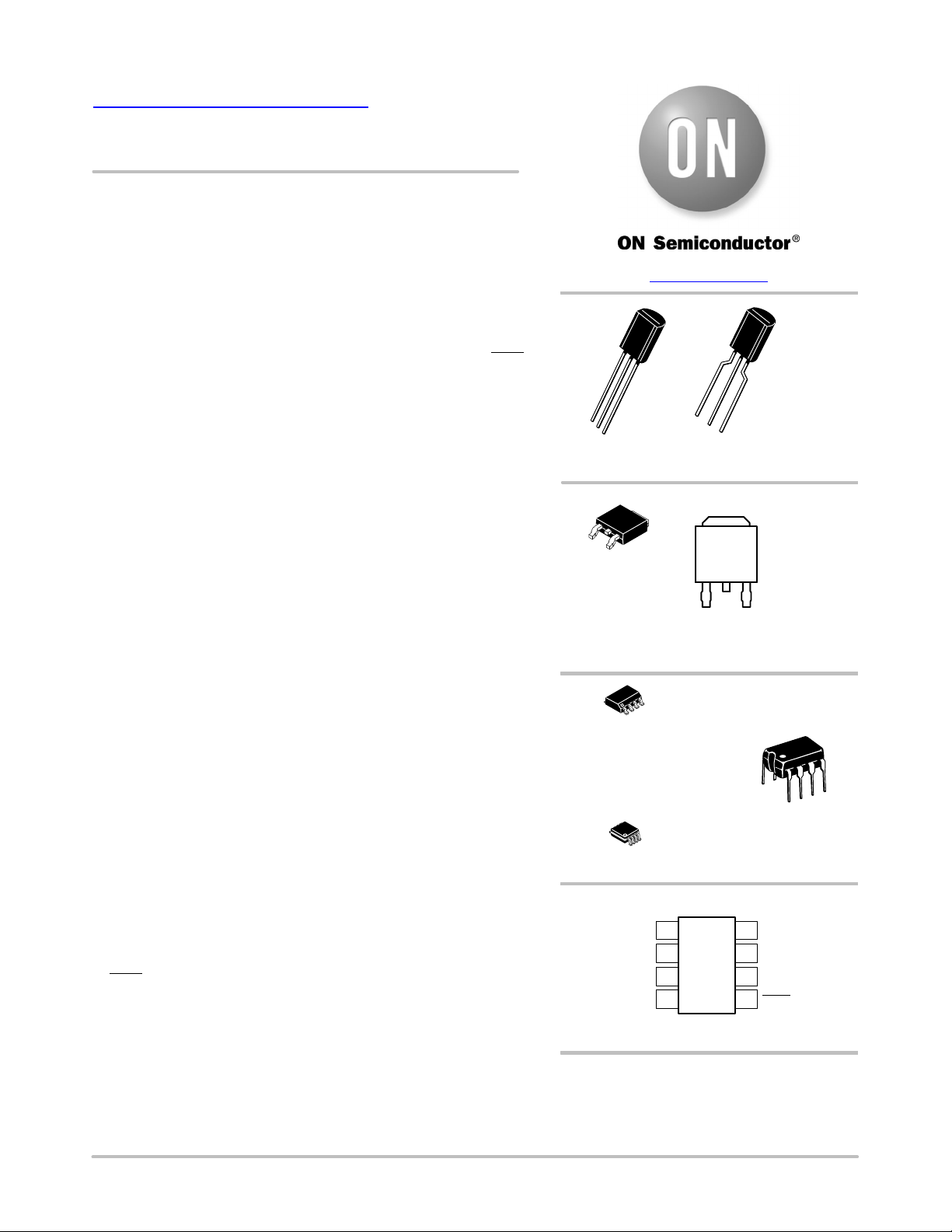
www.onsemi.com
TO−92
CASE 29−10
Pin: 1. Output
1
2
3
4
2
1
3
DPAK
CASE 369C
Heatsink surface (shown as terminal 4 in
case outline drawing) is connected to Pin 2.
1
2
3
BENT LEADSTRAIGHT LEAD
PIN CONNECTIONS
12 3
(Top View)
2. Ground
3. Input
Pin: 1. Input
2. Ground
3. Output
Features
• Low Quiescent Bias Current of 75 mA
• Low Input−to−Output Voltage Differential of 50 mV at 100 mA and
380 mV at 100 mA
• 5.0 V, 3.3 V or 3.0 V ±0.5% Allows Use as a Regulator or Reference
• Extremely Tight Line and Load Regulation
• Requires Only a 1.0 mF Output Capacitor for Stability
• Internal Current and Thermal Limiting
• NCV Prefix for Automotive and Other Applications Requiring
Unique Site and Control Change Requirements; AEC−Q100
Qualified and PPAP Capable
• These Devices are Pb−Free and RoHS Compliant
LP2951 Additional Features
• Error Output Signals an Out of Regulation Condition
• Output Programmable from 1.25 V to 29 V
• Logic Level Shutdown Input
(See Following Page for Device Information.)
8
1
8
1
Output
Sense
Shutdown
GND
ORDERING & MARKING INFORMATION
See detailed ordering and shipping information in the package
dimensions section on pages 14 and 15 of this data sheet.
See general marking information in the device marking
section on page 17 of this data sheet.
SOIC−8
CASE 751
PDIP−8
CASE 626
Micro8E
CASE 846A
PIN CONNECTIONS
18
2
3
4
(Top View)
8
Input
7
Feedback
6
V
5
Error
O
1
Ta p
Output
© Semiconductor Components Industries, LLC, 1995
April, 2021 − Rev. 32
1 Publication Order Number:
LP2950/D
LP2950, LP2951, NCV2951
DEVICE INFORMATION
Output Voltage
Package
TO−92
Suffix Z
DPAK
Suffix DT
SOIC−8 − NCV2951ACD−3.3R2 NCV2951ACDR2 NCV2951CDR2 TA = −40° to +125°C
SOIC−8
Suffix D
Micro8
Suffix DM
DIP−8
Suffix N
LP2950Cx−xx / LP2951Cxx−xx 1% Output Voltage Precision at TA = 25°C
LP2950ACx−xx / LP2951ACxx−xx 0.5% Output Voltage Precision at T
3.0 V 3.3 V 5.0 V Adjustable
LP2950CZ−3.0
LP2950ACZ−3.0
LP2950CDT−3.0
LP2950ACDT−3.0
LP2951CD−3.0
LP2951ACD−3.0
LP2951CDM−3.0
LP2951ACDM−3.0
LP2951CN−3.0
LP2951ACN−3.0
LP2950CZ−3.3
LP2950ACZ−3.3
LP2950CDT−3.3
LP2950ACDT−3.3
LP2951CD−3.3
LP2951ACD−3.3
LP2951CDM−3.3
LP2951ACDM−3.3
LP2951CN−3.3
LP2951ACN−3.3
LP2950CZ−5.0
LP2950ACZ−5.0
LP2950CDT−5.0
LP2950ACDT−5.0
LP2951CD
LP2951ACD
LP2951CDM
LP2951ACDM
LP2951CN
LP2951ACN
= 25°C
A
Not
Available
Not
Available
LP2951CD
LP2951ACD
LP2951CDM
LP2951ACDM
LP2951CN
LP2951ACN
Operating Ambient
Temperature Range
TA = −40° to +125°C
TA = −40° to +125°C
TA = −40° to +125°C
TA = −40° to +125°C
TA = −40° to +125°C
Unregulated DC
Battery or
Unregulated DC
Battery or
Shutdown
From
CMOS/TTL
Input
3
Input 8 Output
Amplifier
3
60 k
50 k
Error Amplifier
GND 2
Error
1.23 V
Reference
1.23 V
Reference
1
75 mV/
60 mV
Error Detection
182 k
60 k
Sense 2
182 k
60 k
Comparator
Output
1
LP2950CZ−5.0
5.0 V/100 mA
1.0 mF
1.0 mF
Tap
V
O
6
7
Feedback
Error
Output
5
LP2951CD or CN
5.0 V/100 mA
330 k
To CMOS/TTL
GND 4
This device contains 34 active transistors.
Figure 1. Representative Block Diagrams
www.onsemi.com
2
LP2950, LP2951, NCV2951
MAXIMUM RATINGS (T
Input Voltage V
Peak Transient Input Voltage (t < 300 ms) V
= 25°C, unless otherwise noted.)
A
Rating
Symbol Value Unit
CC
CC
30 Vdc
32 Vdc
Power Dissipation and Thermal Characteristics
Maximum Power Dissipation P
D
Internally Limited W
Case 751(SOIC−8) D Suffix
Thermal Resistance, Junction−to−Ambient
Thermal Resistance, Junction−to−Case
R
q
JA
R
q
JC
180 °C/W
45 °C/W
Case 369A (DPAK) DT Suffix (Note 1)
Thermal Resistance, Junction−to−Ambient
Thermal Resistance, Junction−to−Case
R
q
JA
R
q
JC
92 °C/W
6.0 °C/W
Case 29 (TO−226AA/TO−92) Z Suffix
Thermal Resistance, Junction−to−Ambient
Thermal Resistance, Junction−to−Case
R
q
JA
R
q
JC
160 °C/W
83 °C/W
Case 626 N Suffix
Thermal Resistance, Junction−to−Ambient
R
q
JA
105 °C/W
Case 846A (Micro8) DM Suffix
Thermal Resistance, Junction−to−Ambient
R
Feedback Input Voltage V
Shutdown Input Voltage V
Error Comparator Output Voltage V
Operating Ambient Temperature Range T
Maximum Die Junction Temperature Range T
Storage Temperature Range T
q
stg
JA
fb
sd
err
A
J
240 °C/W
−1.5 to +30 Vdc
−0.3 to +30 Vdc
−0.3 to +30 Vdc
−40 to +125 °C
+150 °C
−65 to +150 °C
Stresses exceeding those listed in the Maximum Ratings table may damage the device. If any of these limits are exceeded, device functionality
should not be assumed, damage may occur and reliability may be affected.
www.onsemi.com
3
LP2950, LP2951, NCV2951
ELECTRICAL CHARACTERISTICS
(Vin = VO + 1.0 V, IO = 100 mA, CO = 1.0 mF, TA = 25°C [Note 3], unless otherwise noted.)
Characteristic
Output Voltage, 5.0 V Versions V
V
= 6.0 V, I
in
= 100 mA, T
O
= 25°C
A
LP2950C−5.0/LP2951C/NCV2951C* 4.950 5.000 5.050
LP2950AC−5.0/LP2951AC/NCV2951AC* 4.975 5.000 5.025
TA = − 40 to +125°C
LP2950C−5.0/LP2951C/NCV2951C* 4.900 − 5.100
LP2950AC−5.0/LP2951AC/NCV2951AC* 4.940 − 5.060
V
= 6.0 to 30 V, IO = 100 mA to 100 mA, TA = − 40 to +125°C
in
LP2950C−5.0/LP2951C/NCV2951C* 4.880 − 5.120
LP2950AC−5.0/LP2951AC/NCV2951AC* 4.925 − 5.075
Output Voltage, 3.3 V Versions V
V
in
= 4.3 V, I
= 100 mA, T
O
= 25°C
A
LP2950C−3.3/LP2951C−3.3 3.267 3.300 3.333
LP2950AC−3.3/LP2951AC−3.3/NCV2951AC−3.3* 3.284 3.300 3.317
T
= −40 to +125°C
A
LP2950C−3.3/LP2951C−3.3 3.234 − 3.366
LP2950AC−3.3/LP2951AC−3.3/NCV2951AC−3.3* 3.260 − 3.340
V
= 4.3 to 30 V, IO = 100 mA to 100 mA, T
in
= −40 to +125°C
A
LP2950C−3.3/LP2951C−3.3 3.221 − 3.379
LP2950AC−3.3/LP2951AC−3.3/NCV2951AC−3.3* 3.254 − 3.346
Output Voltage, 3.0 V Versions V
V
in
= 4.0 V, I
= 100 mA, T
O
= 25°C
A
LP2950C−3.0/LP2951C−3.0 2.970 3.000 3.030
LP2950AC−3.0/LP2951AC−3.0 2.985 3.000 3.015
TA = − 40 to +125°C
LP2950C−3.0/LP2951C−3.0 2.940 − 3.060
LP2950AC−3.0/LP2951AC−3.0 2.964 − 3.036
V
= 4.0 to 30 V, IO = 100 mA to 100 mA, TA = − 40 to +125°C
in
LP2950C−3.0/LP2951C−3.0 2.928 − 3.072
LP2950AC−3.0/LP2951AC−3.0 2.958 − 3.042
Product parametric performance is indicated in the Electrical Characteristics for the listed test conditions, unless otherwise noted. Product
performance may not be indicated by the Electrical Characteristics if operated under different conditions.
1. The Junction−to−Ambient Thermal Resistance is determined by PCB copper area per Figure 29.
2. This device series contains ESD protection and exceeds the following tests:
Human Body Model (HBM), 2000 V, Class 2, JESD22 A114−C
Machine Model (MM), 200 V, Class B, JESD22 A115−A
Charged Device Model (CDM), 2000 V, Class IV, JESD22 C101−C
3. Low duty pulse techniques are used during test to maintain junction temperature as close to ambient as possible.
4. V
5. Noise tests on the LP2951 are made with a 0.01 mF capacitor connected across Pins 7 and 1.
is the part number voltage option.
O(nom)
6. Latch−up Current Maximum Rating tested per JEDEC standard: JESD78
− Inputs Low: passing positive current 100 mA and negative current −100 mA
− Inputs High: passing positive current 100 mA and negative current −10 mA.
*NCV prefix is for automotive and other applications requiring site and change control.
Symbol Min Typ Max Unit
O
O
O
V
V
V
www.onsemi.com
4
LP2950, LP2951, NCV2951
ELECTRICAL CHARACTERISTICS (continued)
(V
= VO + 1.0 V, IO = 100 mA, CO = 1.0 mF, TA = 25°C [Note 9], unless otherwise noted.)
in
Characteristic
Line Regulation (Vin = V
+1.0 V to 30 V) (Note 10) Reg
O(nom)
LP2950C−XX/LP2951C/LP2951C−XX/NCV2951C* − 0.08 0.20
LP2950AC−XX/LP2951AC/LP2951AC−XX/NCV2951AC* − 0.04 0.10
Load Regulation (IO = 100 mA to 100 mA)
LP2950C−XX/LP2951C/LP2951C−XX/NCV2951C* − 0.13 0.20
LP2950AC−XX/LP2951AC/LP2951AC−XX/NCV2951AC* − 0.05 0.10
Dropout Voltage V
IO = 100 mA
IO = 100 mA − 350 450
Supply Bias Current I
IO = 100 mA
IO = 100 mA − 4.0 12 mA
Dropout Supply Bias Current (V
I
= 100 mA) (Note 10)
O
= V
in
O(nom)
− 0.5 V,
Current Limit (VO Shorted to Ground) I
Thermal Regulation Reg
Output Noise Voltage (10 Hz to 100 kHz) (Note 11) V
CL = 1.0 mF
CL = 100 mF
LP2951A/LP2951AC Only
Reference Voltage (T
= 25°C) V
A
LP2951C/LP2951C−XX/NCV2951C* 1.210 1.235 1.260
LP2951AC/LP2951AC−XX/NCV2951AC* 1.220 1.235 1.250
Reference Voltage (TA = − 40 to +125°C) V
LP2951C/LP2951C−XX/NCV2951C* 1.200 − 1.270
LP2951AC/LP2951AC−XX/NCV2951AC* 1.200 − 1.260
Reference Voltage (TA = − 40 to +125°C) V
IO = 100 mA to 100 mA, Vin = 23 to 30 V
LP2951C/LP2951C−XX/NCV2951C* 1.185 − 1.285
LP2951AC/LP2951AC−XX/NCV2951AC* 1.190 − 1.270
Feedback Pin Bias Current I
Error Comparator
Output Leakage Current (VOH = 30 V) I
Output Low Voltage (Vin = 4.5 V, IOL = 400 mA)
Upper Threshold Voltage (V
Lower Threshold Voltage (V
= 6.0 V) V
in
= 6.0 V) V
in
Hysteresis (Vin = 6.0 V) V
Shutdown Input
Input Logic Voltage
Logic “0” (Regulator “On”) 0 − 0.7
Logic “1” (Regulator “Off”) 2.0 − 30
Shutdown Pin Input Current I
V
= 2.4 V − 35 50
shtdn
V
= 30 V − 450 600
shtdn
Regulator Output Current in Shutdown Mode I
(Vin = 30 V, V
= 2.0 V, VO = 0, Pin 6 Connected to Pin 7)
shtdn
Product parametric performance is indicated in the Electrical Characteristics for the listed test conditions, unless otherwise noted. Product
performance may not be indicated by the Electrical Characteristics if operated under different conditions.
7. The Junction−to−Ambient Thermal Resistance is determined by PCB copper area per Figure 29.
8. ESD data available upon request.
9. Low duty pulse techniques are used during test to maintain junction temperature as close to ambient as possible.
10.V
11.Noise tests on the LP2951 are made with a 0.01 mF capacitor connected across Pins 7 and 1.
is the part number voltage option.
O(nom)
*NCV prefix is for automotive and other applications requiring site and change control.
Symbol Min Typ Max Unit
line
Reg
load
− V
I
O
mV
− 30 80
CC
− 93 120
I
CCdropout
Limit
thermal
n
− 110 170
− 220 300 mA
− 0.05 0.20 %/W
mVrms
− 126 −
− 56 −
ref
ref
ref
− 15 40 nA
− 0.01 1.0
− 150 250 mV
40 45 − mV
− 60 95 mV
− 15 − mV
− 3.0 10
V
V
shtdn
FB
lkg
OL
thu
thl
hy
shtdn
off
%
%
mA
mA
V
V
V
mA
V
mA
mA
www.onsemi.com
5
LP2950, LP2951, NCV2951
DEFINITIONS
Dropout Voltage − The input/output voltage differential
at which the regulator output no longer maintains regulation
against further reductions in input voltage. Measured when
the output drops 100 mV below its nominal value (which is
measured at 1.0 V differential), dropout voltage is affected
by junction temperature, load current and minimum input
supply requirements.
Line Regulation − The change in output voltage for a
change in input voltage. The measurement is made under
conditions of low dissipation or by using pulse techniques
such that average chip temperature is not significantly
affected.
Load Regulation − The change in output voltage for a
change in load current at constant chip temperature.
Maximum Power Dissipation − The maximum total
device dissipation for which the regulator will operate
within specifications.
Bias Current − Current which is used to operate the
regulator chip and is not delivered to the load.
10
1.0
Output Noise Voltage − The RMS ac voltage at the
output, with constant load and no input ripple, measured
over a specified frequency range.
Leakage Current − Current drawn through a bipolar
transistor collector−base junction, under a specified
collector voltage, when the transistor is “off”.
Upper Threshold Voltage − Voltage applied to the
comparator input terminal, below the reference voltage
which is applied to the other comparator input terminal,
which causes the comparator output to change state from a
logic “0” to “1”.
Lower Threshold Voltage − Voltage applied to the
comparator input terminal, below the reference voltage
which is applied to the other comparator input terminal,
which causes the comparator output to change state from a
logic “1” to “0”.
Hysteresis − The difference between Lower Threshold
voltage and Upper Threshold voltage.
6.0
LP2951C
5.0
T
= 25°C
A
4.0
RL = 50 kW
0.1
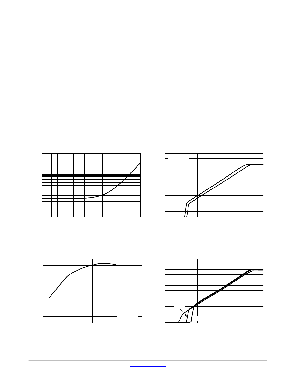
LP2950/LP2951 BIAS CURRENT (mA)
0.01
0.1
1.0 10 100 1.0 2.0 3.0 4.0 5.0 6.0
IL, LOAD CURRENT (mA)
Figure 2. Quiescent Current
5.00
4.99
4.98
4.97
, OUTPUT VOLTAGE (V)
4.96
out
V
4.95
-50
0 50 100 150
T
, AMBIENT TEMPERATURE (°C)
A
Figure 4. Output Voltage versus Temperature
LP2951C
200
3.0
2.0
, OUTPUT VOLTAGE (V)
out
1.0
V
6.0
5.0
4.0
3.0
2.0
, OUTPUT VOLTAGE (V)
out
1.0
V
RL = 50 W
0
0
V
, INPUT VOLTAGE (V)
in
Figure 3. 5.0 V Dropout Characteristics over
Load
LP2951C
25°C
125°C
0
0
−40°C
1.0 2.0 3.0 4.0
, INPUT VOLTAGE (V)
V
in
Figure 5. 5.0 V Dropout Characteristics with
R
= 50 W
L
6.05.0
www.onsemi.com
6
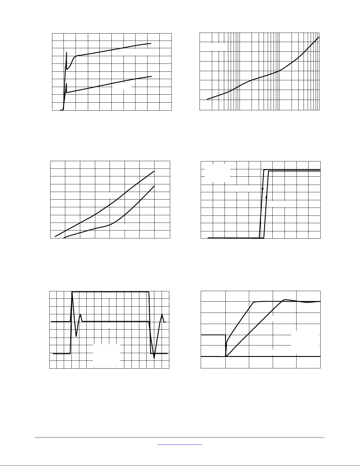
LP2950, LP2951, NCV2951
0
BIAS CURRENT ( A)μ
L
R
DROPOUT VOLTAGE (mV) = 50
550
500
450
400
350
300
250
200
150
100
50
0
-50
400
350
TA = 25°C
0.1 mA Load Current
300
250
200
150
No Load
100
DROPOUT VOLTAGE (mV)
50
0
0
5.0 10 15 20 25
0.1
Vin, INPUT VOLTAGE (V)
Figure 6. Input Current
55
Figure 7. Dropout Voltage versus Output Current
5.0
1.0 10 100
IO, OUTPUT CURRENT (mA)
LP2951C
R
= 330 k
4.0
3.0
2.0
L
T
A
= 25°C
Vin Decreasing
Vin Increasing
RL = 50
50
L
R
45
40
, OUTPUT VOLTAGE (V)
RL = 50 k
0 50 100 150
T, TEMPERATURE (°C)
35
30
DROPOUT VOLTAGE (mV) = 50 k
out
1.0
V
0
4.70
4.74 4.78 4.82 4.86
4.9
Vin, INPUT VOLTAGE (V)
Figure 8. Dropout Voltage versus Temperature Figure 9. Error Comparator Output
8.0
7.5
7.0
6.5
, INPUT VOLTAGE (V)
in
V
6.0
5.5
0
100 200 300
V
in
V
out
TA = 25°C
= 1.0 mF
C
L
I
= 1.0 mA
L
V
= 5.0 V
O
400 500 600 700 800
t, TIME (ms)
4.0
2.0
0
-2.0
-4.0
-6.0
6.0
5.0
4.0
3.0
2.0
1.0
0
OUTPUT VOLTAGE CHANGE (mV)
SHUTDOWN AND OUTPUT VOLTAGE (V)
-1.0
-100
CL = 1.0 mF
CL = 10 mF
Shutdown Input
0 100 200 300 400
t, TIME (ms)
Figure 10. Line Transient Response Figure 11. LP2951 Enable Transient
TA = 25°C
I
= 10 mA
L
V
= 8.0 V
in
V
= 5.0 V
out
www.onsemi.com
7
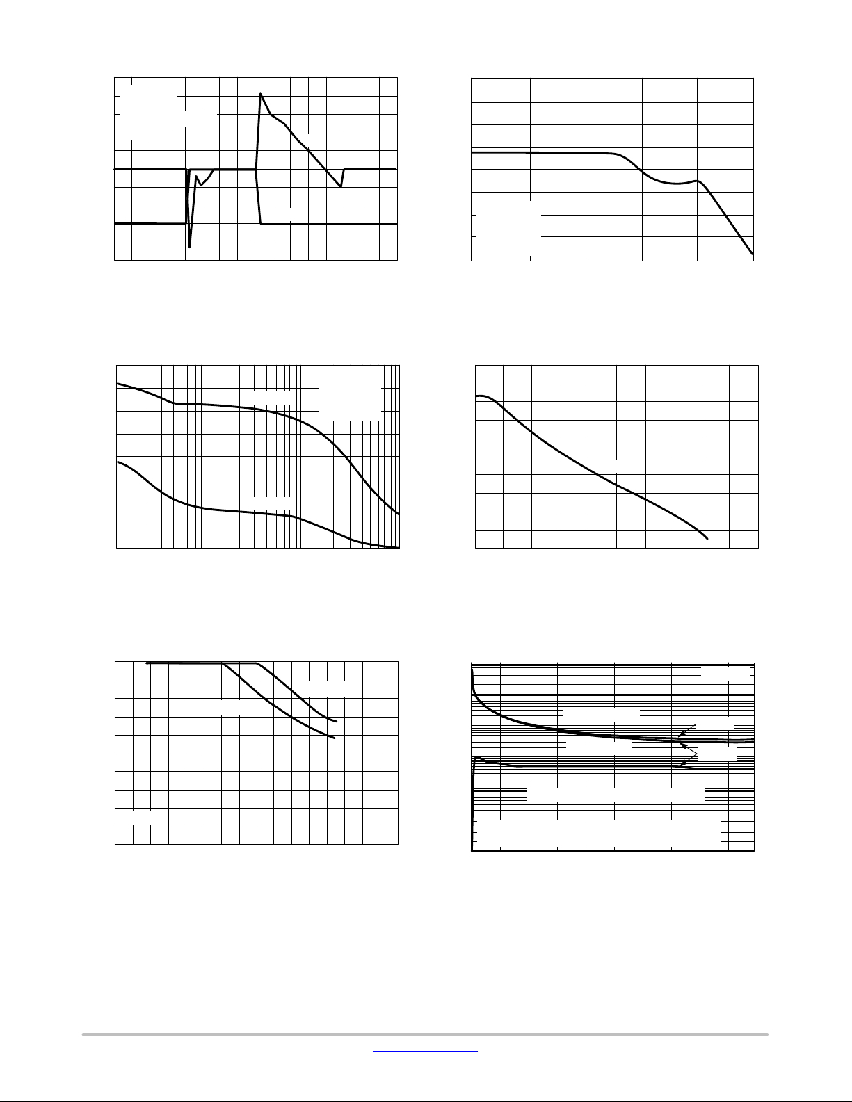
LP2950, LP2951, NCV2951
200
150
100
50
LOAD CURRENT (mA)
-50
4.0
3.0
μ
2.0
1.0
VOLTAGE NOISE ( V/ Hz)√
0
0
CL = 1.0 mF
V
= 5.0 V
out
= 400 mA to 75 mA
I
L
T
= 25°C
A
I
Load
V
t, TIME (ms)
Figure 12. Load Transient Response
CL = 1.0 mF
CL = 100 mF
out
IL= 100 mA
T
A
V
LP2951C
= 25°C
= 5.0 V
O
42.50.5 1.5 2 3 3.51
400
200
0
-200
OUTPUT VOLTAGE CHANGE (mV)
-400
80
60
40
TA = 25°C
20
RIPPLE REJECTION (dB)
= 1.0 mF
C
L
V
= 6.0 V
in
V
= 5.0 V
out
0
1.0
10 100
Figure 13. Ripple Rejection
1.8
1.6
1.4
1.2
1.0
Output “On"
1.0 k
f, FREQUENCY (Hz)
Output “Off"
IL= 0.1 mA
10 k 100 k
100
80
60
40
, OUTPUT CURRENT (mA)
20
out
V
0
100
1.0 k
f, FREQUENCY (Hz)
Figure 14. Output Noise
TA = 75°C
LP2951CN
0
5.0 15 25 35 4010 20 30
0
Vin, INPUT VOLTAGE (V)
Figure 16. Maximum Rated
Output Current
10 k 100 k
TA = 25°C
4.0
2.0
0
-2.0
-4.0
OUTPUT VOLTAGE CHANGE (mV)
-6.0
SHUTDOWN THRESHOLD VOLTAGE (V)
0.8
-20 40 80 120 160
-40
60 100 140200
t, TEMPERATURE (°C)
Figure 15. Shutdown Threshold Voltage
versus Temperature
10000
1000
100
10
Unstable Region
Stable Region
ESR (ohms)
1
0.1
Lower unstable region is for 0.1 mF only.
1 mF and 100 mF show no instability with low ESR values.
0.01
0 102030405060708090100
Unstable Region for 0.1 mF capacitor only
Output Current (mA)
V
out
100 mF
0.1 mF
= 5 V
Figure 17. Output Stability versus Output Capacitor
Change
www.onsemi.com
8

LP2950, LP2951, NCV2951
APPLICATIONS INFORMATION
Introduction
The LP2950/LP2951 regulators are designed with
internal current limiting and thermal shutdown making them
user−friendly. Typical application circuits for the LP2950
and LP2951 are shown in Figures 20 through 28.
These regulators are not internally compensated and thus
require a 1.0 mF (or greater) capacitance between the
LP2950/LP2951 output terminal and ground for stability.
Most types of aluminum, tantalum or multilayer ceramic
will perform adequately. Solid tantalums or appropriate
multilayer ceramic capacitors are recommended for
operation below 25°C.
At lower values of output current, less output capacitance
is required for output stability. The capacitor can be reduced
to 0.33 mF for currents less than 10 mA, or 0.1 mF for currents
below 1.0 mA. Using the 8 pin versions at voltages less than
5.0 V operates the error amplifier at lower values of gain, so
that more output capacitance is needed for stability. For the
worst case operating condition of a 100 mA load at 1.23 V
output (output Pin 1 connected to the feedback Pin 7)
a minimum capacitance of 3.3 mF is recommended.
The LP2950 will remain stable and in regulation when
operated with no output load. When setting the output
voltage of the LP2951 with external resistors, the resistance
values should be chosen to draw a minimum of 1.0 mA.
A bypass capacitor is recommended across the
LP2950/LP2951 input to ground if more than 4 inches of
wire connects the input to either a battery or power supply
filter capacitor.
Input capacitance at the LP2951 Feedback Pin 7 can
create a pole, causing instability if high value external
resistors are used to set the output voltage. Adding a 100 pF
capacitor between the Output Pin 1 and the Feedback Pin 7
and increasing the output filter capacitor to at least 3.3 mF
will stabilize the feedback loop.
Error Detection Comparator
The comparator switches to a positive logic low whenever
the LP2951 output voltage falls more than approximately
5.0% out of regulation. This value is the comparator’s
designed−in offset voltage of 60 mV divided by the 1.235 V
internal reference. As shown in the representative block
diagram. This trip level remains 5.0% below normal
regardless of the value of regulated output voltage. For
example, the error flag trip level is 4.75 V for a normal 5.0 V
regulated output, or 9.50 V for a 10 V output voltage.
Figure 2 is a timing diagram which shows the ERROR
signal and the regulated output voltage as the input voltage
to the LP2951 is ramped up and down. The ERROR
signal
becomes valid (low) at about 1.3 V input. It goes high when
the input reaches about 5.0 V (V
exceeds about 4.75 V).
out
Since the LP2951’s dropout voltage is dependent upon the
load current (refer to the curve in the Typical Performance
Characteristics), the input voltage trip point will vary with
load current. The output voltage trip point does not vary
with load.
The error comparator output is an open collector which
requires an external pullup resistor. This resistor may be
returned to the output or some other voltage within the
system. The resistance value should be chosen to be
consistent with the 400 mA sink capability of the error
comparator. A value between 100 kW and 1.0 MW is
suggested. No pullup resistance is required if this output is
unused.
When operated in the power down mode (V
= 0 V),
in
the error comparator output will go high if it has been pulled
up to an external supply (the output transistor is in high
impedance state). To avoid this invalid response, the error
comparator output should be pulled up to V
out
(see
Figure 18).
5.0 V
Output
Voltage
ERROR
Input
Voltage
Programming the Output Voltage (LP2951)
4.75 V
Not
Valid
4.75 V + V
1.3 V
Figure 18. ERROR Output Timing
dropout
4.70 V
4.70 V + V
dropout
1.3 V
Not
Valid
Pullup
to V
Pullup
to Ext
out
The LP2951CX may be pin−strapped for the nominal
fixed output voltage using its internal voltage divider by
tying Pin 1 (output) to Pin 2 (sense) and Pin 7 (feedback) to
Pin 6 (5.0 V tap). Alternatively, it may be programmed for
any output voltage between its 1.235 reference voltage and
its 30 V maximum rating. An external pair of resistors is
required, as shown in Figure 19.
www.onsemi.com
9

LP2950, LP2951, NCV2951
V
V
in
Error
Output
Shutdown
Input
100 k
5
3
8
V
in
Error
SD
GND FB
47
V
SNS
V
O
1
out
2
NC
R1
6
NC
T
R
2
0.01 mF
V
out
1.23 to 30
3.3 mF
Figure 19. Adjustable Regulator
The complete equation for the output voltage is:
(
1 ) R1ńR2)) IFBR1
ref
FB
where V
V
+ V
out
is the nominal 1.235 V reference voltage and I
ref
is the feedback pin bias current, nominally −20 nA. The
minimum recommended load current of 1.0 mA forces an
upper limit of 1.2 MW on the value of R2, if the regulator
must work with no load. I
in V
which may be eliminated at room temperature by
out
adjusting R1. For better accuracy, choosing R2
will produce a 2% typical error
FB
= 100 k
reduces this error to 0.17% while increasing the resistor
program current to 12 mA. Since the LP2951 typically draws
75 mA at no load with Pin 2 open circuited, the extra 12 mA
of current drawn is often a worthwhile tradeoff for
eliminating the need to set output voltage in test.
for reducing noise on the 3 lead LP2950. However,
increasing the capacitor from 1.0 mF to 220 mF only
decreases the noise from 430 mV to 160 mVrms for a 100 kHz
bandwidth at the 5.0 V output.
Noise can be reduced fourfold by a bypass capacitor
across R1, since it reduces the high frequency gain from 4
to unity. Pick
C
Bypass
[
1
2pR1 x 200 Hz
or about 0.01 mF. When doing this, the output capacitor must
be increased to 3.3 mF to maintain stability. These changes
reduce the output noise from 430 mV to 126 mVrms for a
100 kHz bandwidth at 5.0 V output. With bypass capacitor
added, noise no longer scales with output voltage so that
improvements are more dramatic at higher output voltages.
Unregulated
Input
Error
Output
Shutdown
Input
1.0 mF
10 k
5
Error
LP2951CN
3
SD
GND FB
8
V
in
1
V
out
2
SNS
6
T
V
O
47
0.002 mF
1.0 M
0.01 mF
MTB23P06E
V
5.0 V ±1.0%
0 to 1.0 A
220 mF
2.0 k
out
Output Noise
In many applications it is desirable to reduce the noise
present at the output. Reducing the regulator bandwidth by
increasing the size of the output capacitor is the only method
www.onsemi.com
Figure 20. 1.0 A Regulator with 1.2 V Dropout
10

Unregulated Input
6.0 to 10 Vdc
LP2950, LP2951, NCV2951
TYPICAL APPLICATIONS
+V = 2.0 to 30 V
I
L
Load
I
= 1.23/R
L
GND
2N3906
8
NC
0.1 mF
5
Error
LP2951CN
3
SD
GND FB
47
V
in
1
V
out
2
SNS
6
T
V
O
NC
NC
1N4001
330 pF
2.2 mF
4.2 V ±0.025 V
2.0 M
1.0%
806 k
1.0%
50 k
Figure 21. Lithium Ion Battery Cell Charger
+V
in
470 k
Reset
Normally
Closed
5
470 k
3
8
V
in
Error
LP2951CN
SD
GND FB
47
V
SNS
V
O
1
out
2
NC
6
NC
T
R1
R2
Lithium Ion
Rechargeable
Cell
V
out
1.0 mF
+V
in
Error
Output
Shutdown
Input
47 k
8
V
in
Error
Output
Shutdown
Input
5
Error
LP2951CN
3
SD
V
SNS
V
O
1
out
2
6
T
GND FB
47
R
Figure 22. Low Drift Current Sink
CMOS
*Sleep
Input
5
Error
LP2951CN
3
SD
GND FB
47
Gate
8
V
in
V
out
2
SNS
6
T
V
O
470 k
2N3906
1
NC
NC
200 k
100 k
1.0 mF
100 pF
0.1 mF
V
out
3.3 mF
Error flag occurs when Vin is too
low to maintain V
duced by excessive load current.
out
, or if V
out
is re-
Figure 23. Latch Off When Error Flag Occurs
www.onsemi.com
100 k
Figure 24. 5.0 V Regulator with 2.5 V Sleep Function
11

NC
5
Error
LP2951CN
3
SD
GND FB
LP2950, LP2951, NCV2951
+V
in
8
V
in
1
V
out
2
SNS
#1
47
6
T
V
O
D1
D2
1.0 mF
Memory
V+
20
3.6 V
NiCad
Q1
2N3906
2.7 M
D4
330 k
27 k
5
Error
LP2951CN
3
SD
GND FB
V
#2
D3
8
in
1
V
out
2
SNS
6
T
V
O
Early Warning
Reset
V
DD
Main
Output
1.0 mF
mP
All diodes are 1N4148.
Early Warning flag on low input voltage.
Main output latches off at lower input voltages.
Battery backup on auxiliary output.
Operation: Regulator #1’s V
diode drop above 5.0 V. Its error flag becomes active
when V
error flag of regulator #2 becomes active and via Q1
< 5.7 V. When Vin drops below 5.3 V, the
in
latches the main output “off”. When V
5.7 V, regulator #1 is back in regulation and the early
warning signal rises, unlatching regulator #2 via D3.
47
Figure 25. Regulator with Early Warning and Auxiliary Output
+V
NC
NC
in
0.05
MJE2955
47
R1
4.7 mF
Tant
1000 mF
V
@ 2.0 A
out
100 mF
Error
Flag
2N3906
20 k
Current Limit
Section
680
2N3906
4.7 M
220
5
Error
LP2951CN
3
SD
GND FB
470
10 k
8
V
in
1
V
out
2
SNS
6
T
V
O
.01 mF
47
.33 mF
is programmed one
out
again exceeds
in
0.033 mF
R2
V
= 1.25V (1.0 + R1/R2)
out
For 5.0 V output, use internal resistors. Wire Pin 6 to 7,
and wire Pin 2 to +V
out
Bus.
Figure 26. 2.0 A Low Dropout Regulator
www.onsemi.com
12

LP2950, LP2951, NCV2951
ÎÎÎ
ÎÎÎ
ÎÎÎ
+ 5.0 V
4.7 k
* High for
I
< 3.5 mA
L
360
Output*
20 mA
4
8
15
V
1N4001
NC
NC
0.1 mF
5
Error
LP2951CN
3
SD
Gnd FB
in
V
out
SNS
V
O
1
2
NC
6
T
NC
24
47
1N457
1N457
1N457
Figure 27. Open Circuit Detector for 4.0 to 20 mA Current Loop
2
MC34164P−5
3
100 k
2N3906
8
31.6 k
V
in
5
NC
1
Error
LP2951CN
3
SD
V
SNS
V
O
1
out
2
6
T
Gnd FB
47
NC
Figure 28. Low Battery Disconnect
JAθ
R , THERMAL RESISTANCE
100
90
80
70
60
JUNCTION‐TO‐AIR ( C/W)°
50
40
Free Air
Mounted
Vertically
Minimum
Size Pad
010203025155.0
L, LENGTH OF COPPER (mm)
P
D(max)
R
q
for TA = 50°C
2.0 oz. Copper
L
JA
Figure 29. DPAK Thermal Resistance and Maximum
Power Dissipation versus PCB Copper Length
6.0 V Lead-Acid
Battery
1.0 mF
NC
L
2.4
1.6
1.2
0.8
0.4
0
2.0
20
NiCad Backup
Battery
, MAXIMUM POWER DISSIPATION (W)
D
P
Main V+
Memory V+
www.onsemi.com
13

LP2950, LP2951, NCV2951
ORDERING INFORMATION (LP2950)
Output Voltage
Part Number
LP2950CZ−3.0G 3.0 1.0 TO−92
LP2950CZ−3.0RAG 3.0 1.0 TO−92
LP2950ACZ−3.0G 3.0 0.5 TO−92
LP2950ACZ−3.0RAG 3.0 0.5 TO−92
LP2950CZ−3.3G 3.3 1.0 TO−92
LP2950CZ−3.3RAG 3.3 1.0 TO−92
LP2950ACZ−3.3G 3.3 0.5 TO−92
LP2950ACZ−3.3RAG 3.3 0.5 TO−92
LP2950CZ−5.0G 5.0 1.0 TO−92
LP2950CZ−5.0RAG 5.0 1.0 TO−92
LP2950CZ−5.0RPG 5.0 1.0 TO−92
LP2950ACZ−5.0G 5.0 0.5 TO−92
LP2950ACZ−5.0RAG 5.0 0.5 TO−92
LP2950CDT−3.0G 3.0 1.0 DPAK
LP2950CDT−3.0RKG 3.0 1.0 DPAK
LP2950ACDT−3.0G 3.0 0.5 DPAK
LP2950ACDT−3RKG 3.0 0.5 DPAK
LP2950CDT−3.3G 3.3 1.0 DPAK
LP2950CDT−3.3RKG 3.3 1.0 DPAK
LP2950ACDT−3.3RG 3.3 0.5 DPAK
LP2950CDT−5.0G 5.0 1.0 DPAK
LP2950CDT−5.0RKG 5.0 1.0 DPAK
LP2950ACDT−5.0G 5.0 0.5 DPAK
LP2950ACDT−5RKG 5.0 0.5 DPAK
†For information on tape and reel specifications, including part orientation and tape sizes, please refer to our Tape and Reel Packaging
Specifications Brochure, BRD8011/D.
(Volts)
Tolerance (%) Package Shipping
2000 Units / Bag
(Pb−Free)
2000 Units / Tape & Reel
(Pb−Free)
2000 Units / Bag
(Pb−Free)
2000 Units / Tape & Reel
(Pb−Free)
2000 Units / Bag
(Pb−Free)
2000 Units / Tape & Reel
(Pb−Free)
2000 Units / Bag
(Pb−Free)
2000 Units / Tape & Reel
(Pb−Free)
2000 Units / Bag
(Pb−Free)
2000 Units / Tape & Reel
(Pb−Free)
2000 Units / Ammo Pack
(Pb−Free)
2000 Units / Bag
(Pb−Free)
2000 Units / Tape & Reel
(Pb−Free)
75 Units / Rail
(Pb−Free)
2500 Units / Tape & Reel
(Pb−Free)
75 Units / Rail
(Pb−Free)
2500 Units / Tape & Reel
(Pb−Free)
75 Units / Rail
(Pb−Free)
2500 Units / Tape & Reel
(Pb−Free)
2500 Units / Tape & Reel
(Pb−Free)
75 Units / Rail
(Pb−Free)
2500 Units / Tape & Reel
(Pb−Free)
75 Units / Rail
(Pb−Free)
2500 Units / Tape & Reel
(Pb−Free)
†
www.onsemi.com
14

LP2950, LP2951, NCV2951
ORDERING INFORMATION (LP2951)
Output Voltage
Part Number
LP2951CD−3.0G 3.0 1.0 SOIC−8
LP2951CD−3.0R2G 3.0 1.0 SOIC−8
LP2951ACD−3.0G 3.0 0.5 SOIC−8
LP2951ACD−3.0R2G 3.0 0.5 SOIC−8
LP2951CD−3.3G 3.3 1.0 SOIC−8
LP2951CD−3.3R2G 3.3 1.0 SOIC−8
LP2951ACD−3.3G 3.3 0.5 SOIC−8
LP2951ACD−3.3R2G 3.3 0.5 SOIC−8
LP2951CDG 5.0 or Adj. 1.0 SOIC−8
LP2951CDR2G 5.0 or Adj. 1.0 SOIC−8
LP2951ACDG 5.0 or Adj. 0.5 SOIC−8
LP2951ACDR2G 5.0 or Adj. 0.5 SOIC−8
LP2951CDM−3.0R2G 3.0 1.0 Micro8
LP2951ACDM−3.0RG 3.0 0.5 Micro8
LP2951CDM−3.3R2G 3.3 1.0 Micro8
LP2951ACDM−3.3RG 3.3 0.5 Micro8
LP2951CDMR2G 5.0 or Adj. 1.0 Micro8
LP2951ACDMR2G 5.0 or Adj. 0.5 Micro8
LP2951ACN−3.0G 3.0 0.5 PDIP−8
LP2951CN−3.3G 3.3 1.0 PDIP−8
LP2951ACN−3.3G 3.3 0.5 PDIP−8
LP2951CNG 5.0 or Adj. 1.0 PDIP−8
LP2951ACNG 5.0 or Adj. 0.5 PDIP−8
†For information on tape and reel specifications, including part orientation and tape sizes, please refer to our Tape and Reel Packaging
Specifications Brochure, BRD8011/D.
(Volts)
Tolerance (%) Package Shipping
98 Units / Rail
(Pb−Free)
2500 Units / Tape & Reel
(Pb−Free)
98 Units / Rail
(Pb−Free)
2500 Units / Tape & Reel
(Pb−Free)
98 Units / Rail
(Pb−Free)
2500 Units / Tape & Reel
(Pb−Free)
98 Units / Rail
(Pb−Free)
2500 Units / Tape & Reel
(Pb−Free)
98 Units / Rail
(Pb−Free)
2500 Units / Tape & Reel
(Pb−Free)
98 Units / Rail
(Pb−Free)
2500 Units / Tape & Reel
(Pb−Free)
4000 Units / Tape & Reel
(Pb−Free)
4000 Units / Tape & Reel
(Pb−Free)
4000 Units / Tape & Reel
(Pb−Free)
4000 Units / Tape & Reel
(Pb−Free)
4000 Units / Tape & Reel
(Pb−Free)
4000 Units / Tape & Reel
(Pb−Free)
50 Units / Rail
(Pb−Free)
50 Units / Rail
(Pb−Free)
50 Units / Rail
(Pb−Free)
50 Units / Rail
(Pb−Free)
50 Units / Rail
(Pb−Free)
†
www.onsemi.com
15

LP2950, LP2951, NCV2951
ORDERING INFORMATION (NCV2951)
Output Voltage
Part Number
NCV2951ACD3.3R2G* 3.3 0.5 SOIC−8
NCV2951ACDR2G* 5.0 or Adj. 0.5 SOIC−8
NCV2951CDR2G* 5.0 or Adj. 1.0 SOIC−8
NCV2951ACDMR2G* 5.0 or Adj. 0.5 Micro8
†For information on tape and reel specifications, including part orientation and tape sizes, please refer to our Tape and Reel Packaging
Specifications Brochure, BRD8011/D.
*NCV Prefix for Automotive and Other Applications Requiring Unique Site and Control Change Requirements; AEC−Q100 Qualified and PPAP
Capable.
(Volts)
Tolerance (%) Package Shipping
2500 Units / Tape & Reel
(Pb−Free)
2500 Units / Tape & Reel
(Pb−Free)
2500 Units / Tape & Reel
(Pb−Free)
4000 Units / Tape & Reel
(Pb−Free)
†
www.onsemi.com
16

LP2950, LP2951, NCV2951
MARKING DIAGRAMS
2950
CZ−xx
ALYW
TO−92
CASE 029
2950A
CZ−xx
ALYW
DPAK
CASE 369C
50−yG
ALYWW
SOIC−8
CASE 751
8
51z
ALYW
G
1
8
*
51z−33
ALYW
G
1
50−yyG
ALYWW
8
*
1
51z−3
ALYW
G
50A−yG
ALYWW
50AyyG
ALYWW
8
1
51CN
AWL
YYWWG
8
1
51ACN
AWL
YYWWG
PDIP−8
CASE 626
8
51CN−xx
AWL
YYWWG
1
xx = 3.0, 3.3, or 5.0
y = 3 or 5
yy = 30, 33, or 50
z = A or C
A = Assembly Location
WL, L = Wafer Lot
YY, Y = Year
WW, W = Work Week
G = Pb−Free Package
G = Pb−Free Package
(Note: Microdot may be in either location)
*This marking diagram also applies to NCV2951.
8
51ACN−xx
AWL
YYWWG
1
8
1
CASE 846A
PAy y
AYW G
G
Micro8
8
P−yy
AYW G
G
1
www.onsemi.com
17

MECHANICAL CASE OUTLINE
PACKAGE DIMENSIONS
SCALE 1:1
TO−92 (TO−226) 1 WATT
CASE 29−10
ISSUE D
DATE 05 MAR 2021
1
2
3
1
2
3
BENT LEADSTRAIGHT LEAD
STYLES AND MARKING ON PAGE 3
DOCUMENT NUMBER:
DESCRIPTION:
ON Semiconductor and are trademarks of Semiconductor Components Industries, LLC dba ON Semiconductor or its subsidiaries in the United States and/or other countries.
ON Semiconductor reserves the right to make changes without further notice to any products herein. ON Semiconductor makes no warranty, representation or guarantee regarding
the suitability of its products for any particular purpose, nor does ON Semiconductor assume any liability arising out of the application or use of any product or circuit, and specifically
disclaims any and all liability, including without limitation special, consequential or incidental damages. ON Semiconductor does not convey any license under its patent rights nor the
rights of others.
© Semiconductor Components Industries, LLC, 2019
98AON52857E
TO−92 (TO−226) 1 WATT
Electronic versions are uncontrolled except when accessed directly from the Document Repository.
Printed versions are uncontrolled except when stamped “CONTROLLED COPY” in red.
PAGE 1 OF 3
www.onsemi.com

MECHANICAL CASE OUTLINE
PACKAGE DIMENSIONS
TO−92 (TO−226) 1 WATT
CASE 29−10
ISSUE D
DATE 05 MAR 2021
STYLES AND MARKING ON PAGE 3
DOCUMENT NUMBER:
DESCRIPTION:
ON Semiconductor and are trademarks of Semiconductor Components Industries, LLC dba ON Semiconductor or its subsidiaries in the United States and/or other countries.
ON Semiconductor reserves the right to make changes without further notice to any products herein. ON Semiconductor makes no warranty, representation or guarantee regarding
the suitability of its products for any particular purpose, nor does ON Semiconductor assume any liability arising out of the application or use of any product or circuit, and specifically
disclaims any and all liability, including without limitation special, consequential or incidental damages. ON Semiconductor does not convey any license under its patent rights nor the
rights of others.
© Semiconductor Components Industries, LLC, 2019
98AON52857E
TO−92 (TO−226) 1 WATT
Electronic versions are uncontrolled except when accessed directly from the Document Repository.
Printed versions are uncontrolled except when stamped “CONTROLLED COPY” in red.
PAGE 2 OF 3
www.onsemi.com

TO−92 (TO−226) 1 WATT
CASE 29−10
ISSUE D
DATE 05 MAR 2021
STYLE 1:
PIN 1. EMITTER
2. BASE
3. COLLECTOR
STYLE 6:
PIN 1. GATE
2. SOURCE & SUBSTRATE
3. DRAIN
STYLE 11:
PIN 1. ANODE
2. CATHODE & ANODE
3. CATHODE
STYLE 16:
PIN 1. ANODE
2. GATE
3. CATHODE
STYLE 21:
PIN 1. COLLECTOR
2. EMITTER
3. BASE
STYLE 26:
PIN 1. V
CC
2. GROUND 2
3. OUTPUT
STYLE 31:
PIN 1. GATE
2. DRAIN
3. SOURCE
STYLE 2:
PIN 1. BASE
2. EMITTER
3. COLLECTOR
STYLE 7:
PIN 1. SOURCE
2. DRAIN
3. GATE
STYLE 12:
PIN 1. MAIN TERMINAL 1
2. GATE
3. MAIN TERMINAL 2
STYLE 17:
PIN 1. COLLECTOR
2. BASE
3. EMITTER
STYLE 22:
PIN 1. SOURCE
2. GATE
3. DRAIN
STYLE 27:
PIN 1. MT
2. SUBSTRATE
3. MT
STYLE 32:
PIN 1. BASE
2. COLLECTOR
3. EMITTER
STYLE 3:
PIN 1. ANODE
2. ANODE
3. CATHODE
STYLE 8:
PIN 1. DRAIN
2. GATE
3. SOURCE & SUBSTRATE
STYLE 13:
PIN 1. ANODE 1
2. GATE
3. CATHODE 2
STYLE 18:
PIN 1. ANODE
2. CATHODE
3. NOT CONNECTED
STYLE 23:
PIN 1. GATE
2. SOURCE
3. DRAIN
STYLE 28:
PIN 1. CATHODE
2. ANODE
3. GATE
STYLE 33:
PIN 1. RETURN
2. INPUT
3. OUTPUT
GENERIC
MARKING DIAGRAM*
XXXXX
XXXXX
ALYWG
G
STYLE 4:
PIN 1. CATHODE
2. CATHODE
3. ANODE
STYLE 9:
PIN 1. BASE 1
2. EMITTER
3. BASE 2
STYLE 14:
PIN 1. EMITTER
2. COLLECTOR
3. BASE
STYLE 19:
PIN 1. GATE
2. ANODE
3. CATHODE
STYLE 24:
PIN 1. EMITTER
2. COLLECTOR/ANODE
3. CATHODE
STYLE 29:
PIN 1. NOT CONNECTED
2. ANODE
3. CATHODE
STYLE 34:
PIN 1. INPUT
2. GROUND
3. LOGIC
STYLE 5:
PIN 1. DRAIN
2. SOURCE
3. GATE
STYLE 10:
PIN 1. CATHODE
2. GATE
3. ANODE
STYLE 15:
PIN 1. ANODE 1
2. CATHODE
3. ANODE 2
STYLE 20:
PIN 1. NOT CONNECTED
2. CATHODE
3. ANODE
STYLE 25:
PIN 1. MT 1
2. GATE
3. MT 2
STYLE 30:
PIN 1. DRAIN
2. GATE
3. SOURCE
STYLE 35:
PIN 1. GATE
2. COLLECTOR
3. EMITTER
XXXX = Specific Device Code
A = Assembly Location
L = Wafer Lot
Y = Year
W = Work Week
G = Pb−Free Package
(Note: Microdot may be in either location)
*This information is generic. Please refer to
device data sheet for actual part marking.
Pb−Free indicator, “G” or microdot “G”, may
or may not be present. Some products may
not follow the Generic Marking.
DOCUMENT NUMBER:
DESCRIPTION:
ON Semiconductor and are trademarks of Semiconductor Components Industries, LLC dba ON Semiconductor or its subsidiaries in the United States and/or other countries.
ON Semiconductor reserves the right to make changes without further notice to any products herein. ON Semiconductor makes no warranty, representation or guarantee regarding
the suitability of its products for any particular purpose, nor does ON Semiconductor assume any liability arising out of the application or use of any product or circuit, and specifically
disclaims any and all liability, including without limitation special, consequential or incidental damages. ON Semiconductor does not convey any license under its patent rights nor the
rights of others.
98AON52857E
TO−92 (TO−226) 1 WATT
Electronic versions are uncontrolled except when accessed directly from the Document Repository.
Printed versions are uncontrolled except when stamped “CONTROLLED COPY” in red.
PAGE 3 OF 3
© Semiconductor Components Industries, LLC, 2019
www.onsemi.com

MECHANICAL CASE OUTLINE
PACKAGE DIMENSIONS
2
1
3
SCALE 1:1
L3
L4
b2
GAUGE
L2
PLANE
STYLE 1:
PIN 1. BASE
2. COLLECTOR
3. EMITTER
4. COLLECTOR
STYLE 6:
PIN 1. MT1
2. MT2
3. GATE
4. MT2
4
12 3
e
TOP VIEW
L
DETAIL A
ROTATED 90 CW5
STYLE 7:
5.80
0.228
E
A
b3
4
B
D
NOTE 7
b
0.005 (0.13) C
H
C
L1
PIN 1. GATE
2. COLLECTOR
3. EMITTER
4. COLLECTOR
A1
STYLE 2:
PIN 1. GATE
2. DRAIN
3. SOURCE
4. DRAIN
STYLE 8:
PIN 1. N/C
2. CATHODE
3. ANODE
4. CATHODE
SOLDERING FOOTPRINT*
6.20
0.244
2.58
0.102
DETAIL A
c
SIDE VIEW
M
SEATING
PLANE
STYLE 3:
PIN 1. ANODE
2. CATHODE
3. ANODE
4. CATHODE
3.00
0.118
1.60
0.063
DPAK (SINGLE GAUGE)
CASE 369C
ISSUE F
C
A
c2
H
BOTTOM VIEW
Z
BOTTOM VIEW
ALTERNATE
CONSTRUCTIONS
STYLE 4:
PIN 1. CATHODE
2. ANODE
3. GATE
4. ANODE
STYLE 9:
PIN 1. ANODE
2. CATHODE
3. RESISTOR ADJUST
4. CATHODE
6.17
0.243
STYLE 5:
PIN 1. GATE
2. ANODE
3. CATHODE
4. ANODE
STYLE 10:
PIN 1. CATHODE
2. ANODE
3. CATHODE
4. ANODE
DATE 21 JUL 2015
NOTES:
1. DIMENSIONING AND TOLERANCING PER ASME
Y14.5M, 1994.
2. CONTROLLING DIMENSION: INCHES.
3. THERMAL PAD CONTOUR OPTIONAL WITHIN DIMENSIONS b3, L3 and Z.
4. DIMENSIONS D AND E DO NOT INCLUDE MOLD
FLASH, PROTRUSIONS, OR BURRS. MOLD
FLASH, PROTRUSIONS, OR GATE BURRS SHALL
Z
Z
NOT EXCEED 0.006 INCHES PER SIDE.
5. DIMENSIONS D AND E ARE DETERMINED AT THE
OUTERMOST EXTREMES OF THE PLASTIC BODY.
6. DATUMS A AND B ARE DETERMINED AT DATUM
PLANE H.
7. OPTIONAL MOLD FEATURE.
DIM MIN MAX MIN MAX
A 0.086 0.094 2.18 2.38
A1 0.000 0.005 0.00 0.13
b 0.025 0.035 0.63 0.89
b2 0.028 0.045 0.72 1.14
b3 0.180 0.215 4.57 5.46
c 0.018 0.024 0.46 0.61
c2 0.018 0.024 0.46 0.61
D 0.235 0.245 5.97 6.22
E 0.250 0.265 6.35 6.73
e 0.090 BSC 2.29 BSC
H 0.370 0.410 9.40 10.41
L 0.055 0.070 1.40 1.78
L1 0.114 REF 2.90 REF
L2 0.020 BSC 0.51 BSC
L3 0.035 0.050 0.89 1.27
L4 −−− 0.040 −−− 1.01
Z 0.155 −−− 3.93 −−−
MILLIMETERSINCHES
GENERIC
MARKING DIAGRAM*
XXXXXXG
ALYWW
XXXXXX = Device Code
A = Assembly Location
L = Wafer Lot
Y = Year
WW = Work Week
G = Pb−Free Package
*This information is generic. Please refer
to device data sheet for actual part
marking.
AYWW
XXX
XXXXXG
DiscreteIC
mm
ǒ
SCALE 3:1
inches
Ǔ
*For additional information on our Pb−Free strategy and soldering
details, please download the ON Semiconductor Soldering and
Mounting Techniques Reference Manual, SOLDERRM/D.
DOCUMENT NUMBER:
DESCRIPTION:
ON Semiconductor and are trademarks of Semiconductor Components Industries, LLC dba ON Semiconductor or its subsidiaries in the United States and/or other countries.
ON Semiconductor reserves the right to make changes without further notice to any products herein. ON Semiconductor makes no warranty, representation or guarantee regarding
the suitability of its products for any particular purpose, nor does ON Semiconductor assume any liability arising out of the application or use of any product or circuit, and specifically
disclaims any and all liability, including without limitation special, consequential or incidental damages. ON Semiconductor does not convey any license under its patent rights nor the
rights of others.
© Semiconductor Components Industries, LLC, 2018
98AON10527D
DPAK (SINGLE GAUGE)
Electronic versions are uncontrolled except when accessed directly from the Document Repository.
Printed versions are uncontrolled except when stamped “CONTROLLED COPY” in red.
PAGE 1 OF 1
www.onsemi.com

MECHANICAL CASE OUTLINE
PACKAGE DIMENSIONS
SCALE 1:1
D
14
NOTE 8
TOP VIEW
e/2
A1
D1
e
SIDE VIEW
A
58
H
E1
b2
B
WITH LEADS CONSTRAINED
A2
A
NOTE 3
L
SEATING
PLANE
C
8X
b
M
0.010 CA
MBM
PDIP−8
CASE 626−05
ISSUE P
E
END VIEW
NOTE 5
M
eB
END VIEW
NOTE 6
DATE 22 APR 2015
NOTES:
1. DIMENSIONING AND TOLERANCING PER ASME Y14.5M, 1994.
2. CONTROLLING DIMENSION: INCHES.
3. DIMENSIONS A, A1 AND L ARE MEASURED WITH THE PACKAGE SEATED IN JEDEC SEATING PLANE GAUGE GS−3.
4. DIMENSIONS D, D1 AND E1 DO NOT INCLUDE MOLD FLASH
OR PROTRUSIONS. MOLD FLASH OR PROTRUSIONS ARE
NOT TO EXCEED 0.10 INCH.
5. DIMENSION E IS MEASURED AT A POINT 0.015 BELOW DATUM
PLANE H WITH THE LEADS CONSTRAINED PERPENDICULAR
TO DATUM C.
6. DIMENSION eB IS MEASURED AT THE LEAD TIPS WITH THE
LEADS UNCONSTRAINED.
c
7. DATUM PLANE H IS COINCIDENT WITH THE BOTTOM OF THE
LEADS, WHERE THE LEADS EXIT THE BODY.
8. PACKAGE CONTOUR IS OPTIONAL (ROUNDED OR SQUARE
CORNERS).
INCHES
DIM MIN MAX
A −−−− 0.210
A1 0.015 −−−−
A2 0.115 0.195 2.92 4.95
b 0.014 0.022
b2
0.060 TYP 1.52 TYP
C 0.008 0.014
D 0.355 0.400
D1 0.005 −−−−
E 0.300 0.325
E1 0.240 0.280 6.10 7.11
e 0.100 BSC
eB −−−− 0.430 −−− 10.92
L 0.115 0.150 2.92 3.81
M −−−− 10
MILLIMETERS
MIN MAX
−−− 5.33
0.38 −−−
0.35 0.56
0.20 0.36
9.02 10.16
0.13 −−−
7.62 8.26
2.54 BSC
−−− 10
°°
GENERIC
MARKING DIAGRAM*
STYLE 1:
PIN 1. AC IN
2. DC + IN
3. DC − IN
4. AC IN
5. GROUND
6. OUTPUT
7. AUXILIARY
8. V
CC
DOCUMENT NUMBER:
DESCRIPTION:
98ASB42420B
PDIP−8
XXXXXXXXX
AWL
YYWWG
XXXX = Specific Device Code
A = Assembly Location
WL = Wafer Lot
YY = Year
WW = Work Week
G = Pb−Free Package
*This information is generic. Please refer to
device data sheet for actual part marking.
Pb−Free indicator, “G” or microdot “ G”,
may or may not be present.
Electronic versions are uncontrolled except when accessed directly from the Document Repository.
Printed versions are uncontrolled except when stamped “CONTROLLED COPY” in red.
PAGE 1 OF 1
ON Semiconductor and are trademarks of Semiconductor Components Industries, LLC dba ON Semiconductor or its subsidiaries in the United States and/or other countries.
ON Semiconductor reserves the right to make changes without further notice to any products herein. ON Semiconductor makes no warranty, representation or guarantee regarding
the suitability of its products for any particular purpose, nor does ON Semiconductor assume any liability arising out of the application or use of any product or circuit, and specifically
disclaims any and all liability, including without limitation special, consequential or incidental damages. ON Semiconductor does not convey any license under its patent rights nor the
rights of others.
© Semiconductor Components Industries, LLC, 2019
www.onsemi.com

MECHANICAL CASE OUTLINE
PACKAGE DIMENSIONS
8
1
SCALE 1:1
−Y−
−Z−
−X−
A
58
B
1
4
G
H
D
0.25 (0.010) Z
M
SOLDERING FOOTPRINT*
7.0
0.275
S
Y
0.25 (0.010)
C
SXS
SEATING
PLANE
0.10 (0.004)
1.52
0.060
4.0
0.155
CASE 751−07
M
M
Y
N
SOIC−8 NB
ISSUE AK
K
X 45
_
M
J
MARKING DIAGRAM*
8
XXXXX
ALYWX
1
XXXXX = Specific Device Code
A = Assembly Location
L = Wafer Lot
Y = Year
W = Work Week
G = Pb−Free Package
8
XXXXX
ALYWX
G
1
IC
IC
(Pb−Free)
DATE 16 FEB 2011
NOTES:
1. DIMENSIONING AND TOLERANCING PER
ANSI Y14.5M, 1982.
2. CONTROLLING DIMENSION: MILLIMETER.
3. DIMENSION A AND B DO NOT INCLUDE
MOLD PROTRUSION.
4. MAXIMUM MOLD PROTRUSION 0.15 (0.006)
PER SIDE.
5. DIMENSION D DOES NOT INCLUDE DAMBAR
PROTRUSION. ALLOWABLE DAMBAR
PROTRUSION SHALL BE 0.127 (0.005) TOTAL
IN EXCESS OF THE D DIMENSION AT
MAXIMUM MATERIAL CONDITION.
6. 751−01 THRU 751−06 ARE OBSOLETE. NEW
STANDARD IS 751−07.
MILLIMETERS
DIMAMIN MAX MIN MAX
4.80 5.00 0.189 0.197
B 3.80 4.00 0.150 0.157
C 1.35 1.75 0.053 0.069
D 0.33 0.51 0.013 0.020
G 1.27 BSC 0.050 BSC
H 0.10 0.25 0.004 0.010
J 0.19 0.25 0.007 0.010
K 0.40 1.27 0.016 0.050
M 0 8 0 8
____
N 0.25 0.50 0.010 0.020
S 5.80 6.20 0.228 0.244
INCHES
GENERIC
8
XXXXXX
AYWW
1
Discrete
XXXXXX = Specific Device Code
A = Assembly Location
Y = Year
WW = Work Week
G = Pb−Free Package
8
XXXXXX
AYWW
1
Discrete
(Pb−Free)
G
0.6
0.024
1.270
0.050
SCALE 6:1
ǒ
inches
mm
Ǔ
*This information is generic. Please refer to
device data sheet for actual part marking.
Pb−Free indicator, “G” or microdot “G”, may
or may not be present. Some products may
not follow the Generic Marking.
*For additional information on our Pb−Free strategy and soldering
details, please download the ON Semiconductor Soldering and
Mounting Techniques Reference Manual, SOLDERRM/D.
STYLES ON PAGE 2
DOCUMENT NUMBER:
DESCRIPTION:
ON Semiconductor and are trademarks of Semiconductor Components Industries, LLC dba ON Semiconductor or its subsidiaries in the United States and/or other countries.
ON Semiconductor reserves the right to make changes without further notice to any products herein. ON Semiconductor makes no warranty, representation or guarantee regarding
the suitability of its products for any particular purpose, nor does ON Semiconductor assume any liability arising out of the application or use of any product or circuit, and specifically
disclaims any and all liability, including without limitation special, consequential or incidental damages. ON Semiconductor does not convey any license under its patent rights nor the
rights of others.
© Semiconductor Components Industries, LLC, 2019
98ASB42564B
SOIC−8 NB
Electronic versions are uncontrolled except when accessed directly from the Document Repository.
Printed versions are uncontrolled except when stamped “CONTROLLED COPY” in red.
PAGE 1 OF 2
www.onsemi.com

STYLE 1:
PIN 1. EMITTER
2. COLLECTOR
3. COLLECTOR
4. EMITTER
5. EMITTER
6. BASE
7. BASE
8. EMITTER
STYLE 5:
PIN 1. DRAIN
2. DRAIN
3. DRAIN
4. DRAIN
5. GATE
6. GATE
7. SOURCE
8. SOURCE
STYLE 9:
PIN 1. EMITTER, COMMON
2. COLLECTOR, DIE #1
3. COLLECTOR, DIE #2
4. EMITTER, COMMON
5. EMITTER, COMMON
6. BASE, DIE #2
7. BASE, DIE #1
8. EMITTER, COMMON
STYLE 13:
PIN 1. N.C.
2. SOURCE
3. SOURCE
4. GATE
5. DRAIN
6. DRAIN
7. DRAIN
8. DRAIN
STYLE 17:
PIN 1. VCC
2. V2OUT
3. V1OUT
4. TXE
5. RXE
6. VEE
7. GND
8. ACC
STYLE 21:
PIN 1. CATHODE 1
2. CATHODE 2
3. CATHODE 3
4. CATHODE 4
5. CATHODE 5
6. COMMON ANODE
7. COMMON ANODE
8. CATHODE 6
STYLE 25:
PIN 1. VIN
2. N/C
3. REXT
4. GND
5. IOUT
6. IOUT
7. IOUT
8. IOUT
STYLE 29:
PIN 1. BASE, DIE #1
2. EMITTER, #1
3. BASE, #2
4. EMITTER, #2
5. COLLECTOR, #2
6. COLLECTOR, #2
7. COLLECTOR, #1
8. COLLECTOR, #1
STYLE 2:
PIN 1. COLLECTOR, DIE, #1
2. COLLECTOR, #1
3. COLLECTOR, #2
4. COLLECTOR, #2
5. BASE, #2
6. EMITTER, #2
7. BASE, #1
8. EMITTER, #1
STYLE 6:
PIN 1. SOURCE
2. DRAIN
3. DRAIN
4. SOURCE
5. SOURCE
6. GATE
7. GATE
8. SOURCE
STYLE 10:
PIN 1. GROUND
2. BIAS 1
3. OUTPUT
4. GROUND
5. GROUND
6. BIAS 2
7. INPUT
8. GROUND
STYLE 14:
PIN 1. N−SOURCE
2. N−GATE
3. P−SOURCE
4. P−GATE
5. P−DRAIN
6. P−DRAIN
7. N−DRAIN
8. N−DRAIN
STYLE 18:
PIN 1. ANODE
2. ANODE
3. SOURCE
4. GATE
5. DRAIN
6. DRAIN
7. CATHODE
8. CATHODE
STYLE 22:
PIN 1. I/O LINE 1
2. COMMON CATHODE/VCC
3. COMMON CATHODE/VCC
4. I/O LINE 3
5. COMMON ANODE/GND
6. I/O LINE 4
7. I/O LINE 5
8. COMMON ANODE/GND
STYLE 26:
PIN 1. GND
2. dv/dt
3. ENABLE
4. ILIMIT
5. SOURCE
6. SOURCE
7. SOURCE
8. VCC
STYLE 30:
PIN 1. DRAIN 1
2. DRAIN 1
3. GATE 2
4. SOURCE 2
5. SOURCE 1/DRAIN 2
6. SOURCE 1/DRAIN 2
7. SOURCE 1/DRAIN 2
8. GATE 1
SOIC−8 NB
CASE 751−07
ISSUE AK
STYLE 3:
STYLE 7:
STYLE 11:
STYLE 15:
STYLE 19:
STYLE 23:
PIN 1. DRAIN, DIE #1
2. DRAIN, #1
3. DRAIN, #2
4. DRAIN, #2
5. GATE, #2
6. SOURCE, #2
7. GATE, #1
8. SOURCE, #1
PIN 1. INPUT
2. EXTERNAL BYPASS
3. THIRD STAGE SOURCE
4. GROUND
5. DRAIN
6. GATE 3
7. SECOND STAGE Vd
8. FIRST STAGE Vd
PIN 1. SOURCE 1
2. GATE 1
3. SOURCE 2
4. GATE 2
5. DRAIN 2
6. DRAIN 2
7. DRAIN 1
8. DRAIN 1
PIN 1. ANODE 1
2. ANODE 1
3. ANODE 1
4. ANODE 1
5. CATHODE, COMMON
6. CATHODE, COMMON
7. CATHODE, COMMON
8. CATHODE, COMMON
PIN 1. SOURCE 1
2. GATE 1
3. SOURCE 2
4. GATE 2
5. DRAIN 2
6. MIRROR 2
7. DRAIN 1
8. MIRROR 1
PIN 1. LINE 1 IN
2. COMMON ANODE/GND
3. COMMON ANODE/GND
4. LINE 2 IN
5. LINE 2 OUT
6. COMMON ANODE/GND
7. COMMON ANODE/GND
8. LINE 1 OUT
STYLE 27:
PIN 1. ILIMIT
2. OVLO
3. UVLO
4. INPUT+
5. SOURCE
6. SOURCE
7. SOURCE
8. DRAIN
DATE 16 FEB 2011
STYLE 4:
PIN 1. ANODE
2. ANODE
3. ANODE
4. ANODE
5. ANODE
6. ANODE
7. ANODE
8. COMMON CATHODE
STYLE 8:
PIN 1. COLLECTOR, DIE #1
2. BASE, #1
3. BASE, #2
4. COLLECTOR, #2
5. COLLECTOR, #2
6. EMITTER, #2
7. EMITTER, #1
8. COLLECTOR, #1
STYLE 12:
PIN 1. SOURCE
2. SOURCE
3. SOURCE
4. GATE
5. DRAIN
6. DRAIN
7. DRAIN
8. DRAIN
STYLE 16:
PIN 1. EMITTER, DIE #1
2. BASE, DIE #1
3. EMITTER, DIE #2
4. BASE, DIE #2
5. COLLECTOR, DIE #2
6. COLLECTOR, DIE #2
7. COLLECTOR, DIE #1
8. COLLECTOR, DIE #1
STYLE 20:
PIN 1. SOURCE (N)
2. GATE (N)
3. SOURCE (P)
4. GATE (P)
5. DRAIN
6. DRAIN
7. DRAIN
8. DRAIN
STYLE 24:
PIN 1. BASE
2. EMITTER
3. COLLECTOR/ANODE
4. COLLECTOR/ANODE
5. CATHODE
6. CATHODE
7. COLLECTOR/ANODE
8. COLLECTOR/ANODE
STYLE 28:
PIN 1. SW_TO_GND
2. DASIC_OFF
3. DASIC_SW_DET
4. GND
5. V_MON
6. VBULK
7. VBULK
8. VIN
DOCUMENT NUMBER:
DESCRIPTION:
ON Semiconductor and are trademarks of Semiconductor Components Industries, LLC dba ON Semiconductor or its subsidiaries in the United States and/or other countries.
ON Semiconductor reserves the right to make changes without further notice to any products herein. ON Semiconductor makes no warranty, representation or guarantee regarding
the suitability of its products for any particular purpose, nor does ON Semiconductor assume any liability arising out of the application or use of any product or circuit, and specifically
disclaims any and all liability, including without limitation special, consequential or incidental damages. ON Semiconductor does not convey any license under its patent rights nor the
rights of others.
© Semiconductor Components Industries, LLC, 2019
98ASB42564B
SOIC−8 NB
Electronic versions are uncontrolled except when accessed directly from the Document Repository.
Printed versions are uncontrolled except when stamped “CONTROLLED COPY” in red.
PAGE 2 OF 2
www.onsemi.com

MECHANICAL CASE OUTLINE
PACKAGE DIMENSIONS
SCALE 2:1
Micro8
CASE 846A−02
ISSUE K
DATE 16 JUL 2020
GENERIC
MARKING DIAGRAM*
8
XXXX
AYW G
G
1
XXXX = Specific Device Code
A = Assembly Location
Y = Year
W = Work Week
G = Pb−Free Package
(Note: Microdot may be in either location)
*This information is generic. Please refer to
device data sheet for actual part marking.
Pb−Free indicator, “G” or microdot “G”, may
or may not be present. Some products may
not follow the Generic Marking.
STYLE 1:
PIN 1. SOURCE
2. SOURCE
3. SOURCE
4. GATE
5. DRAIN
6. DRAIN
7. DRAIN
8. DRAIN
STYLE 2:
PIN 1. SOURCE 1
2. GATE 1
3. SOURCE 2
4. GATE 2
5. DRAIN 2
6. DRAIN 2
7. DRAIN 1
8. DRAIN 1
STYLE 3:
PIN 1. N-SOURCE
2. N-GATE
3. P-SOURCE
4. P-GATE
5. P-DRAIN
6. P-DRAIN
7. N-DRAIN
8. N-DRAIN
DOCUMENT NUMBER:
DESCRIPTION:
ON Semiconductor and are trademarks of Semiconductor Components Industries, LLC dba ON Semiconductor or its subsidiaries in the United States and/or other countries.
ON Semiconductor reserves the right to make changes without further notice to any products herein. ON Semiconductor makes no warranty, representation or guarantee regarding
the suitability of its products for any particular purpose, nor does ON Semiconductor assume any liability arising out of the application or use of any product or circuit, and specifically
disclaims any and all liability, including without limitation special, consequential or incidental damages. ON Semiconductor does not convey any license under its patent rights nor the
rights of others.
© Semiconductor Components Industries, LLC, 2019
98ASB14087C
MICRO8
Electronic versions are uncontrolled except when accessed directly from the Document Repository.
Printed versions are uncontrolled except when stamped “CONTROLLED COPY” in red.
PAGE 1 OF 1
www.onsemi.com

ON Semiconductor and are trademarks of Semiconductor Components Industries, LLC dba ON Semiconductor or its subsidiaries in the United States and/or other countries.
ON Semiconductor owns the rights to a number of patents, trademarks, copyrights, trade secrets, and other intellectual property. A listing of ON Semiconductor’s product/patent
coverage may be accessed at www.onsemi.com/site/pdf/Patent−Marking.pdf
ON Semiconductor makes no warranty, representation or guarantee regarding the suitability of its products for any particular purpose, nor does ON Semiconductor assume any liability
arising out of the application or use of any product or circuit, and specifically disclaims any and all liability, including without limitation special, consequential or incidental damages.
Buyer is responsible for its products and applications using ON Semiconductor products, including compliance with all laws, regulations and safety requirements or standards,
regardless of any support or applications information provided by ON Semiconductor. “Typical” parameters which may be provided in ON Semiconductor data sheets and/or
specifications can and do vary in different applications and actual performance may vary over time. All operating parameters, including “Typicals” must be validated for each customer
application by customer’s technical experts. ON Semiconductor does not convey any license under its patent rights nor the rights of others. ON Semiconductor products are not
designed, intended, or authorized for use as a critical component in life support systems or any FDA Class 3 medical devices or medical devices with a same or similar classification
in a foreign jurisdiction or any devices intended for implantation in the human body. Should Buyer purchase or use ON Semiconductor products for any such unintended or unauthorized
application, Buyer shall indemnify and hold ON Semiconductor and its officers, employees, subsidiaries, affiliates, and distributors harmless against all claims, costs, damages, and
expenses, and reasonable attorney fees arising out of, directly or indirectly, any claim of personal injury or death associated with such unintended or unauthorized use, even if such
claim alleges that ON Semiconductor was negligent regarding the design or manufacture of the part. ON Semiconductor is an Equal Opportunity/Affirmative Action Employer. This
literature is subject to all applicable copyright laws and is not for resale in any manner.
. ON Semiconductor reserves the right to make changes without further notice to any products herein.
PUBLICATION ORDERING INFORMATION
LITERATURE FULFILLMENT:
Email Requests to: orderlit@onsemi.com
ON Semiconductor Website: www.onsemi.com
TECHNICAL SUPPORT
North American Technical Support:
Voice Mail: 1 800−282−9855 Toll Free USA/Canada
Phone: 011 421 33 790 2910
Europe, Middle East and Africa Technical Support:
Phone: 00421 33 790 2910
For additional information, please contact your local Sales Representative
◊
www.onsemi.com
1
 Loading...