

Page 1

AN.No.G1216B1N000-3D0E
LIQUID CRYSTAL DISPLAY MODULE
G 1 2 1 6 B 1 N 0 0 0
USER’S MANUAL
Seiko Instruments Inc.
Page 2

AN.No.G1216B1N000-3D0E
This manual provides technical information covering functions and operational
instructions for the G1216 liquid crystal display modules made by Seiko
Instruments Inc. Pleas e read throu gh this m anual bef ore oper ating the product.
Distribution of this manual to third parties for a n y purpose other than operat io n of
the product is prohib ited. The descrip tions herein are s ubject to cha nge without
prior notice.
Version
1 Original December 1993
Copyright
Printed in Japan
1993 by Seiko Instruments Inc.
Revision Record
Revision Date
- i -
Page 3

CONTENTS
1. GENERAL
1.1 General..................................................................................................... 1
1.2 Features.................................................................................................... 1
1.3 Absolute Maximum Ratings (excluding LED backlight)............................ 2
1.4 Mechanical Characteristics....................................................................... 2
1.5 Electrical Characteristics (excluding LED backlight) ............................... 2
1.6 Optical Characteristics.............................................................................. 3
1.7 LC Panel Life Time................................................................................... 4
1.8 LED Backlight Characteristics .................................................................. 4
1.9 Dimensions............................................................................................... 6
2. CIRCUIT CONFIGURATION
AN.No.G1216B1N000-3D0E
2.1 Block Diagram .......................................................................................... 7
2.2 Segment Drivers (HD61202).................................................................... 7
2.3 Common Driver (HD61203)...................................................................... 13
2.4 Bias Vo lta ge Ge nerat or ............................................................................ 13
3. OPERATING INSTRUCTIONS
3.1 Terminal Functions................................................................................... 14
3.2 Timing Characteristics.............................................................................. 15
3.3 Reset Function ......................................................................................... 16
3.4 Instructions ............................................................................................... 17
3.5 Contrast Adjustment and Power Supply Example ................................... 21
3.6 LED Backlight Driver Example ................................................................. 21
3.7 MPU Con necti on Dia gram........................................................................ 23
4. PRECAUTIONS................................................................................................... 24
INDEX
- ii -
Page 4

AN.No.G1216B1N000-3D0E
GENERAL
1.
1.1 General
The G1216 is a very thin LCD module on whic h a f ul l-dot matrix LCD panel and a CMOS IC driver are
integrated. The LCD panel used here featur es wide viewing angle and high contr ast. This full dot
configuration allo ws a wide variet y of patterns to be disp layed depending u pon the input data. The
display position is the intersection point of the matrix transparent electrodes. This prevents displa y
distortion and displacem ent. Incorporating a display RAM and a disp lay timing signal generator into
the G1216 allows for direct connection with the MPU circuit without using an LCD controller.
1.2 Features
12864 full dot matrix configuration
1/64 duty, 1/9 bias
Two 4096-bit internal display data RAMs
An internal display timing signal generator
8-bit parallel interfac e
Instructions:
Display Data Read/Write, Display ON/OFF, Display Start Line, X-Address (Page) Set, Y- Address
Set, and Status Read.
Three types of power supply: VDD= +5 V, VLC , LEDA (LED anode)
Transflective, gray mode
Positive display
Display data “H”: Display ON: blue display color
Display data “L”: Display OFF: gray background
A wide operating temperature rang e
A built-in LED backlight (color: yellow-green)
- 1 -
Page 5
1.3 Absolute Maximum Ratings (excluding LED backlight)
Item Symbol Conditions Min. Max. Unit
AN.No.G1216B1N000-3D0E
Vss = 0 V
Power supply
voltage
Input voltage
Operating
temperature
Storage
temperature
Storage
humidity
V
DD
V
LC
V
IN
T
opr
T
stg
Ta = 25C
5010%RH
65%RH
48 hrs
1000 hrs
1.4 Mechanical Characteristics
Item Standard
Dot configuration 12864 dot
Module dimensions ( H V T ) [ mm ] 75.0 52.7 8.9
Viewing area ( H V ) [ mm ] 60.0 32.5
Active display area ( H V ) [ mm ] 55.01 27.49
Dot dimensions ( H V ) [ mm ] 0.4 0.4
Dot pitch ( H V ) [ mm ] 0.43 0.43
Weight [ g ] 45 max.
H : Horizontal V : Vertical T : Thickness (max.)
V
-
DD
-0.3
-20
-30
+20
+20
0.3
-19.0
V
V
7.0
DD
DD
+70
+80
+85
+65
+ 0.3
+ 0.3
V
V
V
C
C
%RH
%RH
1.5 Electrical Characteristics (excluding LED backlight)
V
= 5 V5%, VSS = 0 V, Ta = -20C to +70C
DD
Item Symbol UnitMin. Typ. Max.
Input
voltage
Input
voltage
Output
voltage
Power supply voltage
Current
consumption
Frame fr equency
1
Applied to RST.
2
Applied to DB0 to DB7, E, R/W, D/I, CS1 and CS2.
3
Applied to DB0 to DB7.
4
Display patterns: checkered patterns.
High
1
Low
High
2
Low
High
3
Low
4
V
V
V
V
V
V
V
V
f
IHC
ILC
IHT
ILT
OH
DD
I
DD
I
LC
FRM
OL
LC
Conditions
=- 205 A
I
OH
= 1.6 mA
I
OL
=5 V, Ta = 25C
V
DD
= 8.0
V
LC
0.7
0
2.0
0
2.4
4.75
-12.0
V
DD
5.00
-8.0
2.0
1.8
71.4
V
0.3V
V
0.8
0.4
5.25
-3.0
3.0
3.0
DD
DD
DD
V
V
V
V
V
V
V
V
mA
mA
H
Z
- 2 -
Page 6
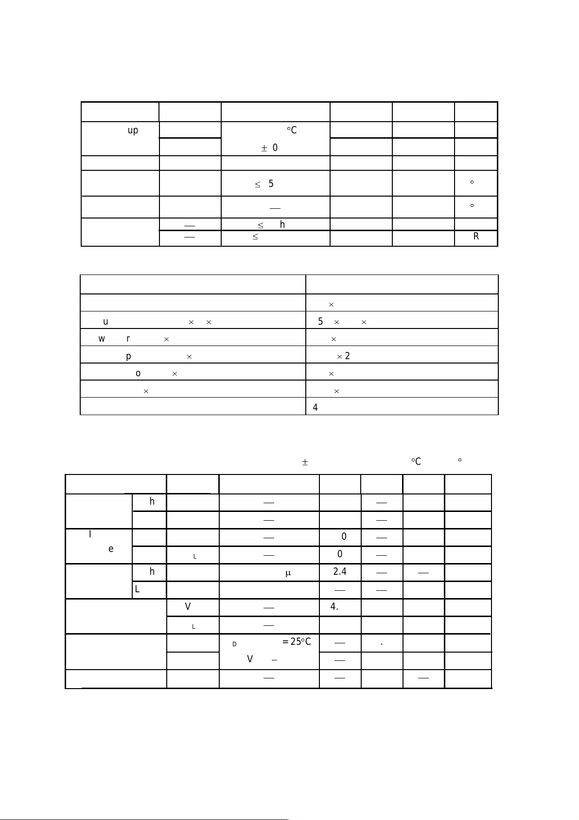
1.6 Optical Characteristics
Vopr=14.0 V
Vopr=13.0 V
off
Vopr=13.0 V
1
θ2θ
θ2θ
θ
∅
AN.No.G1216B1N000-3D0E
1/64 duty, 1/9 bias, f
= 71.4 Hz, Vopr = VDD -VLC , LED backlight: OFF
FRM
Item Sym. Conditions RemarkMin.Temp. Typ. Max.
15
30
50
70
Viewing angle
θ
θ
θ2-θ
θ
θ
θ2-θ
1
2
1
1
2
C ≥ 2.0
∅ = 0°
Vopr=13.0 V
C ≥ 2.0
∅ = 270°
Vopr=13.0 V
25°C
25°C
θ = 0°
Contrast
Response time
∅ = 0°
t
t
t
θ = 0°
on
∅ = 0°
off
θ = 0°
on
∅ = 0°
t
25°CC
25°C
-20°C
2300
Measuring instrument : Canon illuminometer LC-3S
Note 1: Definition of angle θ and
Note 2: Definition of viewing angles θ 1
and θ 2
40
100
630
-15
-20
3.52.5
100
200
1000
3500
Unit
Degree
ms
Refer to notes
1 and 2
Note 3
Note 4
Light
(reflective LCD)
Y’(∅=180°)
X’
Z (θ=0°)
Z’
Sensor
Cmax.
Contrast C
1
2.0
LCD panel
X (∅=90°)
1
∅
Y (∅=0°)
(θ=90°)
Remark: The optimum viewing angle by visual
inspection and angle θ at Cmax do
Viewing angle
not always match.
Page 7
AN.No.G1216B1N000-3D0E
t
t
Selected status
Non-selected status
°
C
−
30 to +80
T
stg
Storage temp. range
−
Note 3: Definition of contrast (C)
C =
Brightness
(reflection)
Brightness of non-selected dot (reflection) B
Brightness of selected dot (reflection) B1
(%)
0
Operating
voltage(V)
1.7 LC panel life time
Item Unit
Note 4: Definition of response time
V
100%
opr
1/f
FRM
(display ON)
90%
on
(display OFF)
10%
off
(V)
2
Brightness for selected
B
2
B
1
dot
Brightness
curve for nonselected dot
Non-selected
status
Light
Brightness
Dark
V
: Operating voltage ton: Response time (rise)
opr
f
: Frame frequency tof: Response time (fall)
FRM
Note: Measurement must be made using a transmissive LCD panel.
Conditions Standard
Life time
1
Definition of life time: the time up to occurrence of any of the following:
Contrast reduces to 30% of the initial value.
ž
Current consumption becomes three times the initial value.
ž
Orientation deteriorates significantly.
ž
The display malfunctions.
ž
1
25°C±10°C
<65%RH
1.8 LED backlight characteristics
(1) Absolute maximum ratings
Item Symbol Standard Unit
DC forward current
DC reverse voltage
Allowable dissipation
Operating temp. range
I
F
V
R
P
D
T
opr
200*
8
860
20 to +70
−
mA
V
mW
C
°
* Forward current reduction characteristics: The absolute maximum rating of the forward current
varies depending on ambient temperature.
hrs100,000 or more
IF ( mA )
200
50
20
70
Ta (°C)25
Page 8
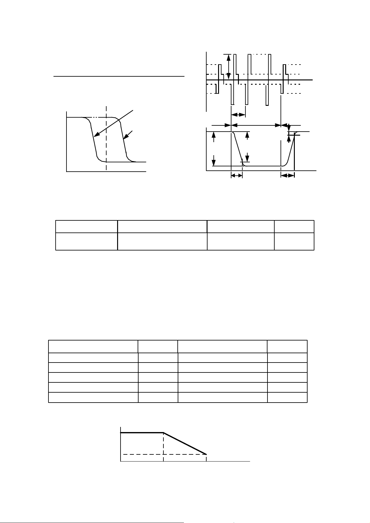
(2) Electrical and optical characteristics
1
AN.No.G1216B1N000-3D0E
Ta = 25°C
Item
Forward voltage
Reverse current
Symbol
V
F
I
R
Meas. condition Max.Typ.Min. Unit
IF=90 mA
VR=8 V
(3) LED backlight connection diagram
(4) Brightness (panel upper side)
Item
Surface brightness
(Center of LCD panel)
Symbol
B
P
Measurement conditions and a measuring instrument are:
Ta=25°C±3°C
ž
30 to 85%RH
ž
IF= 90 mA
ž
f
=71.4 Hz
ž
FRM
VLC: Optimum LC drive voltage
ž
Display OFF (Entire display data=“L”)
ž
Measured 30 minutes after LED lights
ž
Measuring instrument: BM - 7 (TOPCON)
ž
3.8
4.1
4.4
0.9
V
mA
LEDA
Number of LED
chips=20
LEDC
Max.Typ.Min. Unit
2.01.0
nit
(5) Life time
Item Measurement conditions Standard Unit
Life time
1
Ta=25°C±10°C
IF=90 mA
hrs50,000 or more
Definition of life time: The time until the brightness decreases to one half the initial
brightness.
Page 9
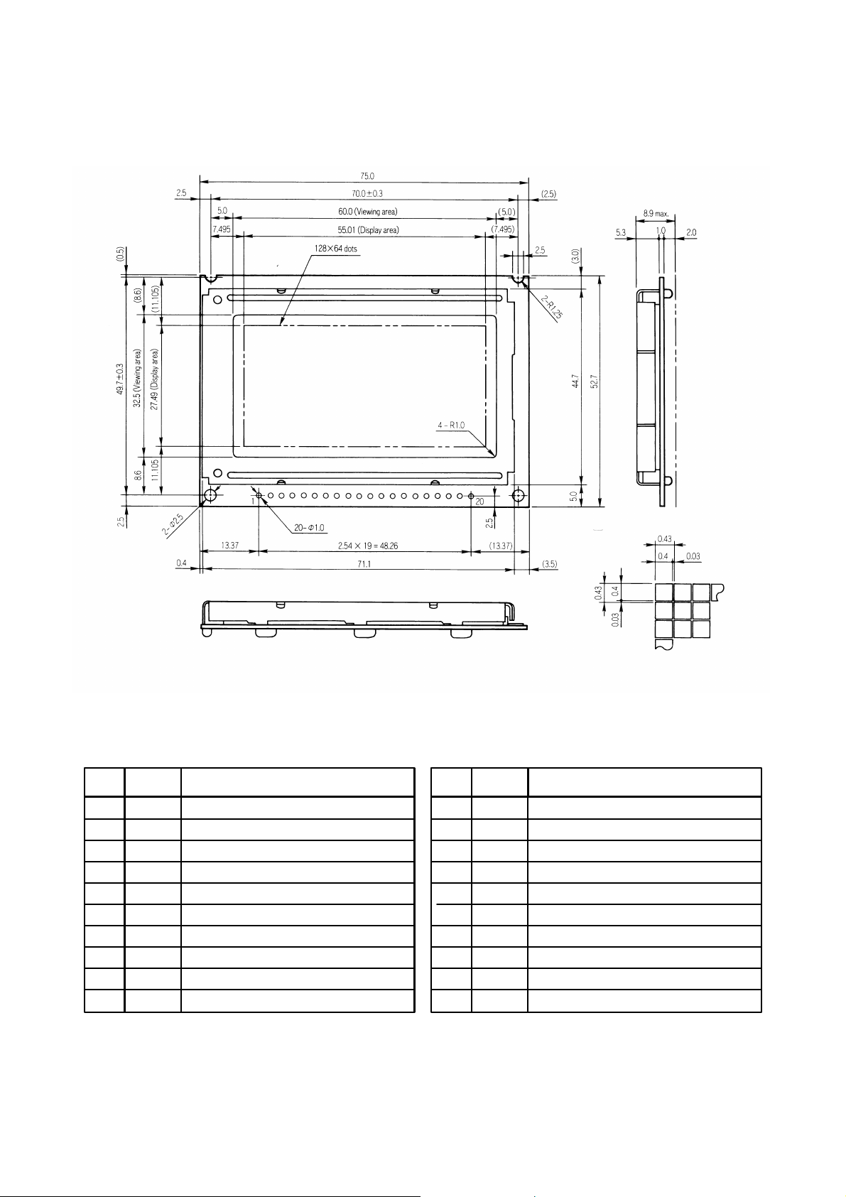
1.9 Dimensions
1
AN.No.G1216B1N000-3D0E
Unit: mm
General dimensional tolerance:±0.5
I/O terminal functions
Sym.No.
V
1
V
2
V
3
DB
4
DB
5
DB
6
DB
7
DB
8
DB
9
10
F
DB
is connected to the metallic frame of the module. Use this frame when grounding.
GND
Power supply voltage: +5.0 V
DD
GND: 0 V
SS
LC drive voltage
LC
Data bus (LSB)
0
Data bus
1
Data bus
2
Data bus
3
Data bus
4
Data bus
5
Data bus
6
Functions
Figure 1 Dimensions
11
12
13
14
15
16
17
18
19
20
DB
CS1
CS2
RST
R/W
D/I
E
F
GND
LEDA
LEDC
Data bus (MSB)
7
Chip select (1)
Chip select (2)
Reset
Read/Write
Data/Instruction
Enable
Frame ground
LED anode
LED cathode
FunctionsSym.No.
1
Page 10

AN.No.G1216B1N000-3D0E
g
2. CIRCUIT CONFIGURATION
2.1 Block Diagram
This product consists of two HD61202 segment drivers, an HD61203 common driver and a bias
voltage generator. Figure 2 shows the block diagram.
DB
to DB
0
7
RST, R/W, D / I, E
CS2
CS1
V
LC
V
DD
V
SS
Bias Voltage
Generator
V
a
V
b
V
e
V
f
Va, Vc, Vd, V
FRM
M
CL2
1
2
f
Segment Driver 1
64
Segment Driver 2
64
Common Driver
64
12864 full dot matrix LCD
LEDA
LED Backlight
LEDC
Fi
ure 2 Block Diagram
2.2 Segment Drivers (HD61202)
The segment driver is a 64 drive output CMOS IC. The G1216 is driven wit h the panel d ivided into
two right and left displays. A segm ent driver controls the divided s creen. 8 bits of data transm itted
from the MPU are saved in the internal display RAM, an d t he s e gment signal is gener ate d to dri ve t he
LC. 1 bit of display RAM data corresponds to 1 dot lighting or non-lighting on the LC panel.
- 7 -
Page 11

2.2.1 Block Diagram (Segment Driver)
AN.No.G1216B1N000-3D0E
RST
V
DD
Busy Flag
Display ON/OFF
V
SS
V
LC
CS R/W D/I
E
DB0 to DB
8
7
Segment Dr iver
Interface Control
Input and Output Buffer
8
Output
Register
6
Display Start Line
Register
8
Input
Register
8
Instruction Register
9
X, Y-Address
Counter
Z-Address
Counter
6
8
Display Data RAM
6
4096 bit
9
64
Display Data Latch
64
4
LC Driver
V
M
2
1
FRM
CL
a
V
c
V
d
V
f
Y1 Y2
Y64
Figure 3 Segment Driver
- 8 -
Page 12

AN.No.G1216B1N000-3D0E
2.2.2 Functions and Operations of Main Blocks
(1) Interface Control Unit
The interface control unit consists of the following blocks:
Input and output buffer
Input and output register
Instruction register
The above blocks are selected according to the following combinations of R/W and D/I signals:
D / I R / W Functions
1 1 Output Register Read
Internal Operation (Display Data RAM Output Register)
10
Input Register Write
Internal Operation (Input Resister Display Data RAM)
0 1 Busy Check and Status Read
0 0 Instruction
Input and output buffer
The data is transmitted through eight data buses (DB
DB
....... MSB (most significant bit)
7
DB
...... LSB (least significant bit)
0
to DB7).
0
The data can be input and output on ly when the Ch ip Select is selected. T herefore, if the Ch ip Se lect
is not selected, the internal condition remains unchanged and instruction will not be executed, even
when changing the signal of the input terminals excluding the RST (reset) terminal.
Note that the RST operates regardless of CS1 and CS2.
Input and output register
This product is prov ided with an inp ut register and an output register s o that the product can interface
with MPUs having speed differing from the internal operation.
Input register
The input register is a register that is used for temporarily storing the data to be written in the display
data RAM. The data to be written f rom the MPU to the i nput regis ter will be autom aticall y writte n in
the display data RAM through internal operation.
When the Chip Select is selected and R / W = 0, D / I =0, the data is written in the register,
synchronized with the fall of signal E.
Output register
The output register is a register that is used for temporaril y storing the data to be read from the
display data RAM.
- 9 -
Page 13

AN.No.G1216B1N000-3D0E
In order to read the con tent of the outp ut register, t he Chip Sel ect must be s elected, D/I mus t be 1,
and R/W must be 1. W hen executing the “Read” instruction, the contents of the output register
stored at that time are output during the time that “E” is 1. When “E” falls, display data of the
currently indicated addres s is written in the output register. Af ter that, the address advances b y
one.
The contents of the output regist er are r e wr itte n by the Read instruct ion. T he data is retained b y the
address set or other instructions. Ac cordingl y, when perf orm ing the address s et, and nex t executi ng
the Read instruction, the data of the specified address is not output and the data of the address
which is specified is output at the second dat a read time. Therefore, when setting the addres s, a
dummy read is needed once. See Figure 4.
D / I
R/W
E
Address
Output Re gister
DB0 to DB
N N+1
N address data
Busy
Check
7
Address
Set
(Address
N)
Busy
Check
Data Read
(dummy)
Busy
Check
Data Read
(N address
data)
N+2
N+1 address data
Busy
Check
Data Read
(N+1 address
data)
Figure 4 Read Timing
(2) Busy flag
The status when busy flag is “1” means that t he module is operatin g internally. Ins tructions ot her than
he Status Read are not available at this time. The busy flag is output to DB
by the Status Read
7
instruction. Ensure that the busy flag is “0” before executing the instruction.
E
F is freq uency of
BUSY
1
F
1 or 2
T
BUSY
3
F
(1 / 2 the s ource osci llation frequenc y of HD61203): 215 kHz typ.
T
BUSY
Figure 5 Busy Flag
(3) Display ON/OFF Flip/Flop
The display ON/OFF Flip/Flop is a flip-flop function that determines whether the display data
corresponding to the R AM data is outp ut to the segm ent on the LCD (ON status ) or goes to all nonl it
status regardless of the RAM data (O FF status). This is co ntrolled b y the d isplay ON /OFF instruct ion.
When the RST signal bec omes “0,” the display goes to OFF status. This f lip- f lop s tat us is o utpu t to DB
by the Status Read instruction.
Even when performing display ON/OFF, the data inside the RAM is not affected.
- 10 -
5
Page 14

AN.No.G1216B1N000-3D0E
(4) Display start line register
The display start line register is a regis ter which determ ines the line address (see Fi gure 6) for which
data is displayed on the top line of the LCD screen when displayin g the contents of the displa y data
RAM on the LCD screen. It is also used to scroll the display. The 6 bit (0 to 63) display start line
information is written in this register by the Display Start Line Set Instruction.
The contents of this register are transmitted to address counter Z at “H” level of the FRM signal
(common driver output) which indicates the display start on the screen.
(5) Z-address counter
The Z-address counter generates the address to output the display data synchronized with the
common signal. This is a 6-bit counter which c ou nts at t he f al l of th e CL signal (common dr iver output).
The contents of the display start line register are preset to the Z-address counter at “ H” level of the
FRM signal (common driver output).
(6) Displa y data RAM
The display data RAM is a RAM that stores the disp lay dot data. 1 bit of RAM data correspon ds to
lighting (data=1) or non-lighting ( data = 0) of 1 dot of the display on th e LCD screen. Fig ure 6 s hows
the relationship between the ad dress and dat a insid e the R AM on e ither the rig ht or left s creen (6464
dots). In this case, the display start line is 0.
- 11 -
Page 15

AN.No.G1216B1N000-3D0E
Y
Y61Y62Y
X=0
g
Display pattern
(Display star t line: 0)
Common driver
output
X
to X
1
64
Segment driver output
Y
to Y
1
Data inside
display RAM
DB0(LSB)
DB
DB
DB
DB
DB
DB
DB7(MSB)
COM1
COM2
COM3
COM4
COM5
COM6
COM7
COM8
COM9
COM62
COM63
COM64
64
62 63 641 2 3 4 5
Line addr es s
0
1
1
1
0
1
0
0
0
1
1
2
3
4
5
6
0
1
0
1
1
1
0
1
0
0
1
0
0
1
0
0
1
1
1
1
0
0
1
0
0
1
0
0
0
0
0
0
1
Line 0
0
0
1
Line 1
0
0
1
Line 2
1
0
1
0
1
1
0
0
1
0
0
1
0
0
00
0
0
0
X- address
(page)
X=1
X=2
0 1 0 0
0
1 0 0 0
1 1 1 1 1
0 0 0 0 0
Y-address
ure 6 Relationship Between Displ ay and Data Inside Display RAM
Fi
0 Y1 Y2 Y3 Y4
0
0
0
0
0
0
0
Line 62
0
Line 63
63
0
0
X=7
(7) X, Y- address counter
X, Y-address counter is a 9-bit counter which gives the address of the interna l display dat a RAM. It is
necessary to set the X -address counter of the thre e upper bits, and the Y-address counter of the six
lower bits using differ ing instr uc ti ons .
X-address counter
Address counter X is a sim ple reg ister that is n ot pr ovide d with a cou nt functio n. T he addres s is set
by instruction.
- 12 -
Page 16

AN.No.G1216B1N000-3D0E
O
l
Y-address counter
This counter sets the address by instruction and is automatically advanced by the read/write
operation. Counting is performed by looping the values 0 to 63.
2.3 Common driver (HD61203)
The common driver is a 64 drive output CMOS IC. Incorporating an oscillation circuit, this driver
generates the comm on signal and timing signa ls (LC AC drive contro l, and one-frame tim ing signal)
necessary for the LC d isplay, a nd controls the dis play by supp lying t he tim ing s ignals t o the segm ent
drivers.
2.4 Bias voltage generator
Six levels of standard voltag e Va to Vf are applied to the dr ivers as a bias vo ltage. This voltag e is
generated by resistance division of Vopr and driven by a voltage follower through an operational
amplifier.
V
DD
R
1
R
1
R
V
opr
V
LC
2
R
1
R
1
+
+
+
+
perationa
Amplifier
C
C
C
C
C
1 / 9 bias: R2= (9 4) R1= 5 R
V
a
V
b
V
c
V
d
V
e
V
f
1
Figure 7 Bias Voltage Generator
- 13 -
Page 17

3. OPERATING INSTRUCTIONS
Chi
ibl
CS1: C
LCM left half displ
(SEG1
3.1 Terminal Functions
AN.No.G1216B1N000-3D0E
Table 1 Terminal Functions
Signal
to
DB
0
E 1
DB
QTY
7
8 I/O MPU
I/O
Destination
Input MPU
R/W 1 Input MPU
D/I 1 Input MPU
CS1, CS2 2 Input MPU
Functions
Common terminal for tristate input and output, and data bus.
Enable
Write (R/W=0):Latches data of DB
Read (R/W=1):Outputs data to DB
to DB7 at the fall of E.
0
to DB7 while “E” keeps a
0
high level.
Read/Write selection
R/W=1: Wh en E=1 and CS1= 0 or CS2=0, the data is outpu t
to DB
to DB7 and read is available by MPU.
0
R/W=0: Wh en CS1=0 or CS2 = 0, DB
to DB7 are ready for
0
receiving the input.
Data/Instruction selection
D/I=1: Indicates that the data in DB
to DB7 is the display
0
data.
D/I=0: Indicates that the data in DB
to DB7 is the instruction
0
code.
p select input. Data input and output is poss
e under
the following sta tus:
LCM display screen
Terminal No.
Status
CS1
0
CS2
0
CS2CS1
RST 1 Input MPU
V
DD
V
SS
V
LC
LEDA 1
LEDC 1
F
GND
1
F
terminal is connected to the metallic frame of the module. Use this terminal when
GND
1
1
1
1
grounding the frame.
SEG64).
ontrols the
CS2: Contr ols the LCM right half disp lay scr ee n (SEG65 to
SEG128).
Reset si gn al
Setting the RST signal to a low level allows for initial setup.
(1) ON /OFF register: 0 setup (display OFF)
(2) Display st art line register: 0 lin e s etup (dis play starts
from 0 lin e)
The setup status is retained until the status is changed by an
instruction after reset is released.
Power Power terminal for logic (+5 V)
Power GND terminal (0 V)
Power Power terminal for LC drive
Power LED backlight anode terminal
Power LED backlight cathode terminal
Frame ground
1
ay screen
to
- 14 -
Page 18

3.2 Timing Characteristics
D
AN.No.G1216B1N000-3D0E
NoteunitMax.Typ.Min.SymbolItem
E cycle time
E pulse width (H)
E pulse width (L)
E rise time
E fall time
Address setup time
Address hold time
Data setup time
Data delay time
Data hold time during write
Data hold time during read
Note 1: When t he MPU writes:
t
CYC
P
P
t
r
t
f
t
AS
t
AH
t
DSW
t
DDR
t
DHW
t
DHR
WEH
WEL
1000
450
450
140
10
200
10
20
320
25
25
ns
ns
ns
ns
ns
ns
ns
ns
ns
ns
ns
Note 2: When t he MPU reads:
1, 2
1, 2
1, 2
1, 2
1, 2
1, 2
1, 2
1
2, 3
1
2
t
CYC
2.0V
E
0.8V
R / W
CS1, CS2
D/I
DB0 to DB
7
2.0V
0.8V
2.0V
0.8V
P
WEL
t
AS
t
AS
2.0V
0.8V
P
WEH
t
r
Note 3: Load circuits (DB0 to DB7)
D
1
Test point
C R
t
DSW
t
CYC
t
f
t
AH
t
AH
t
DHW
R
L
RL= 2.4 k
R=11 k
2
D
3
D
4
C = 130 pF (including jig capacity)
Diodes D1 to D4 are 1S2074 H .
2.0V
E
0.8V
R / W
CS1, CS2
D/I
DB0 to DB
7
2.0V
0.8V
2.0V
0.8V
P
WEL
t
AS
t
AS
P
WEH
DDR
2.4V
0.4V
t
f
t
AH
t
AH
t
DHR
t
r
t
- 15 -
Page 19

3.3 Reset Function
Setting the RST terminal to a low level when the power is on allows for initial setup.
Display OFF
Display start line register: Set address 0.
While the RST remains at a low level, instructions other than the status read cannot be accepted.
AN.No.G1216B1N000-3D0E
Execute other instructions after confirming that DB
=0 (reset release) and DB7=0 (ready) , using the
4
status read instruction.
The power conditions for power-on initial setup are as follows:.
Item
Reset time
Rise time
Symbol
t
RST
t
r
Min
1.0
Typ.
Max
200
unit
ns
s
4.5V
V
DD
RST
t
RST
t
r
0.7V
0.3V
DD
DD
If the RESET is executed during operation, retention of the contents of all registers (excluding an
ON/OFF register) and the RAM is not guaranteed. Always set them again.
- 16 -
Page 20

AN.No.G1216B1N000-3D0E
3.4 Instructions
3.4.1 General
Instructions are listed on Table 2. Instructions other than the Status Read instruction will not be
executed if they are sent while another instruction is already being execut ed. The busy flag is “1”
when executing the instruction. Check whether or not the flag is “1” before transmitting the
instructions from the MPU.
Table 2 List of Instructions
Instruction
Display
1
ON / OFF
Display start
2
line
X-address
(page) set
3
Y-address
4
set
Status read
5
Display data
6
write
Display data
7
read
Code
R/W D / I DB7DB6DB5DB4DB3DB2DB1DB
0 0 0 0 1 1 1 1 1 1/0
0 0 1 1
0 0 1 0 1 1 1
0 0 0 1
B
1 0
0 1 Write Data
1 1 Read Data
U
S
Y
ON
/
0
OFF
Display start lines
( 0 to 63 )
X-address(page)
Y-address
( 0 to 63 )
R
E
S
0 0 0
E
T
(0 to 7)
Function
0
Turns ON / OFF total display. Data and
internal status in the display RAM remain
unchanged.
1: ON 0 : OFF
Determines the RAM line to be displayed on the
top line (COM1) on the display.
Sets the X-address of the RAM (page) in the
X-address (page) register.
Set Y-address of the RAM in the Y-address
counter.
Reads the status.
RESET 1: Reset 0: Normal
ON/OFF 1: Display OFF 0: Display ON
0
BUSY 1: during internal operation
0: READY status
Writes data DB0 (LSB) to
(MSB ) on the data
DB
7
bus into the display RAM.
Reads data DB0 (LSB) to
(MSB) from the
DB
7
display RAM into the data
bus.
Accesses the
RAM in which
address has been
specified
beforehand. After
that the Y-address
advances by one.
Note: The BUSY time varies depending upon the frequency F (:215 kHz (typ.) ) of 1, 2 (1/F T
BUSY
3/F).
3.4.2 Detailed explanation
(1) Display ON/OFF
D/I DB
Code
R/W
0 0
7
0 0 1 1 1 1 1 D
DB
0
Turns the display ON when D=1, and OFF when D=0 . When the display is tur ned OFF by D=0, the
original display appears if D is set to 1 because the display data is retained in the display data RAM.
- 17 -
Page 21

AN.No.G1216B1N000-3D0E
(2) Display start line
D/I DB
Code
R/W
0 0
7
1 1 A A A A A A
Upper bits
Lower bits
DB
0
Sets the display data RAM line address expressed with binary AAAAAA in the display start line
register. When disp laying the content of the display data RAM, th e d isplay data on t he line addresses
which are set in the register is displayed on the top line on the LCD s c reen . For a ddr es s c onf iguration
inside the display data, refer to Figure 6. Figure 8 shows display examples of start lines 0 to 3.
COM1
COM2
COM3
COM4
COM5
COM6
COM7
COM8
COM9
COM10
-
-
COM59
COM60
COM61
COM62
COM63
COM64
COM1
COM2
COM3
COM4
COM5
COM6
COM7
COM8
COM9
COM10
-
-
COM59
COM60
COM61
COM62
COM63
COM64
Display start line=0
COM1
COM2
COM3
COM4
COM5
COM6
COM7
COM8
COM9
COM10
-
-
COM59
COM60
COM61
COM62
COM63
COM64
Display start line=1
COM1
COM2
COM3
COM4
COM5
COM6
COM7
COM8
COM9
COM10
-
-
COM59
COM60
COM61
COM62
COM63
COM64
Display start line
=2
Display start line=3
Figure 8 Relationship Between Display Start Lines and Displays
- 18 -
Page 22

AN.No.G1216B1N000-3D0E
(3) X-address (page) set
D/I DB
Code
R/W
0 0
7
1 0 1 1 1 A A A
Upper bits
Lower bits
DB
0
The display data RAM “X ” address (pa ge) whic h is expres sed with binary AAA is set in the X -addr ess
register. Following write/read operations from the MPU are performed on the specified X-address
(page) until the next X-addres s (page) set is perform ed. The conf iguration of dis play data RA M and
X-address is shown in Figure 9.
D/I DB
Code
R/W
0 0
7
0 1 A A A A A A
Upper bits Lower bits
DB
0
(4) Y-address set
The display data RAM Y- ad dress which is expressed with binar y AAAAAA is set in the Y-addr ess
counter. After that th e Y-address counter a dvances by one eac h time write/r ead is perf ormed from
the MPU. The configuration of the display data RAM and Y-address is shown in Figure 9.
Y-address
01234---------------616263
DB
0
to
DB
DB
to
DB
DB
to
DB
DB
to
DB
7
0
7
0
7
0
7
Page 0
Page 1
Page 6
Page 7
X=0
X=1
X=6
X=7
Figure 9 Display Data RAM Address Configuration
- 19 -
Page 23

AN.No.G1216B1N000-3D0E
(5) Status read
D/I DB
Code
R/W
1 0 0
7
BUSY
ON/OFF
RESET
0 0 0 0
DB
0
BUSY: When BUSY=1, it means that the the module is operating internally and the next instruction is
not accepted until BUSY=0. After confirming that BUSY=0, it is necessary to perform the
next write.
ON/OFF: Indicates that the display is OFF when ON/OFF=1.
Indicates that the display is ON when ON/OFF=0.
RESET: Indicates that initial setup is performed by the RST signal.
Indicates that the initialization is being performed when RESET=1 and instructions other than
the Status Read instruction are not accepted.
When RESET=0, initialization is completed and operation status is normal.
(6) Display data write
D/I DB
Code
R/W
0 1
7
D D D D D D D D
Upper bits
Lower bits
DB
0
Writes 8-bit binary data DDDDDDDD in the displa y data RAM. After the write is completed, th e Yaddress is automatically advanced by one
(7) Display data read
D/I DB
code
R/W
1 1
7
D D D D D D D D
Upper bits
Lower bits
DB
0
Read 8-bit binary data DDDDDDDD from the display data RAM. After read is performed, the Yaddress is automatical ly advanced by one. A dummy read is nec essary once, imm ediately after the
address set is completed. For details, refer to segment driver output register section.
- 20 -
Page 24

AN.No.G1216B1N000-3D0E
−
−
3.5 Contrast Adjustment and Power Supply Example
The LC panel viewing angle and display screen contrast are greatly affected by the ambient
temperature. The recommended LC drive voltage (Vopr) at each temperature is given below. Vopr
is a value at which the best display is visually obtained. This value does not always correspond to the
value at which the best contrast (Cmax.) is obtained. A contrast adjustment circuit example is shown
below:
V
Temperature (°C)
20
0
25
50
70
opr
= V
DD
V
LC
Voltage (V
5V
12 V
C2
opr
)
13.5
13.0
12.5
C1
R
A
R
V
R
B
Figure 10 Contrast Adjustment
3.6 LED Backlight Driver Examples
(1) Example 1
A basic LED backlight driver example is shown in Figure 11.
VIN = +5V
R=30Ω, (≥1/4W)
11.5
V
DD
V
SS
V
LC
LEDA
G1216
10.5
RA=10 k
Ω
RB=1.2 k
RV (variable resistor)
=10 k
Ω
C1, C2=10 µF
Ω
LEDC
G1216
Figure 11 LED Backlight Driver Example 1
Where resistance “R” is the limit resistance of the LED forward current. The forward current depends
upon the temperature. Especially, it must be decreased at high temperature. For temperature
dependence, refer to forward current reduction characteristics described in 1.8 (1). The operating
temperature for the G1216 ranges from −20°C to +70°C. It is necessary to determine limit resistance
“R” so that the forward current becomes 50 mA or lower at +70°C.
Forward voltage VF at each temperature of the LED backlight is shown in Table 3.
Table 3 Forward Voltage At Temperatures
Temperature (Ta) Conditions VF min. VF typ. VF max.
−20°C IF=90 mA 3.9 V 4.3 V 4.6 V
+25°C IF=90 mA 3.8 V 4.1 V 4.4 V
+70°C IF=50 mA 3.5 V 3.7 V 3.9 V
Page 25

AN.No.G1216B1N000-3D0E
−
Limit resistance “R” is calculated using the following equation. The resistance becomes the value
shown in Figure 11.
VIN=Input voltage (power voltage)(V)
VF=LED forward voltage (V)
IF=Allowable LED forward current (A)
R=
V
V
IN
F
I
(Ω)
F
For this resistance value, the forward current becomes lower than 50 mA at 25°C. The surface
brightness of the LED backlight varies with the forward current. See Figure 12. Compared with 1.8 (4)
brightness (IF=90 mA), the brightness is about 40%.
1.2
1.0
0.8
Relative
brightness
0.6
0.5
0.4
0.2
Forward current:
30 40 50 60 70 80 90 100 110
IF(mA)
Figure 12 Forward Current-Brightness Characteristics (Ta=25°C)
(2) Example 2
When you want to keep the brightness (2 nit) at 25°C, use a thermosensitive element, like a thermistor,
and a transistor as shown in Figure 13. Set the thermosensitive element to about IF=90 mA at 25°C
and configure it so that “IF” will be reduced as the temperature rises.
LEDA
R2
V
IN
LEDC
G1216
Tr
R3
Thermistor
R1
R4
Figure 13 LED Backlight Driver Example 2
Page 26

3.7 MPU Connection Diagram
AN.No.G1216B1N000-3D0E
Z80A
D0 to D7
A0 to A15
RD
IORQ
M1
INT
Decoder
A0
A1
D0 to D7
CE
C / D
A / B
RD
IORQ
M1
INT
Z80 PIO
A0 to A7
B0
B1
B2
B3
B4
B5
G1216
DB0 to DB
E
R/W
D/I
RST
CS1
CS2
V
DD
V
SS
V
LC
7
Figure 14 Example of Connection to Z80A
- 23 -
Page 27

AN.No.G1216B1N000-3D0E
4
. PRECAUTIONS
Safety
If the LCD panel is damaged, be careful not to get the liquid crystal in your mouth. If the liquid
crystal touches your skin or clothes, promptly wash it off using soap and plenty of water.
Handling
Avoid static electricity, as it will damage the CMOS LSI.
The LCD panel is made of plate glass. Do not hit or crush it.
Do not remove the panel or frame from the module.
The polarizer of the display is very fragile. Handle it very carefully.
Mounting and design
Mount the module by using the specified mounting parts and holes.
To protect the module against external pressure, place a transparent plate (e.g., acrylic or glass)
on the module, leaving a small gap between the display surface and transparent plate.
Example
✩
Small gap
Exterior face
Transparent plate
Module
Screw
Design the system so that no input signal is given unless the power-supply voltage is applied.
Keep the module dry. Avoid condensation to prevent the transparent electrodes from being
damaged.
Storage
Store the module in a dark place, where the temperature is 25C 10C and the relative humidity
below 65%.
Do not store the module near organic solvents or corrosive gases.
Keep the module (including accessories) safe from vibration, shock and external pressure.
Cleaning
Do not wipe the polarizer with a dry cloth, as it may scratch the surface.
Wipe the module gently with a soft cloth soaked with a petroleum benzine.
Do not use ketonic (ketone) solvents (ketone and acetone) or aromatic solvents (toluene and
xylene), as they may damage the polarizer.
- 24 -
Page 28

INDEX
AN.No.G1216B1N000-3D0E
- A -
Active display area ............................................................................. 2
- B -
Bias voltage generator .................................................................7, 13
Block diagram................................................................................. 7, 8
Busy flag....................................................................................... 8, 10
- C -
Chip select................................................................................ 6, 9, 14
Cleaning ........................................................................................... 24
Common driver............................................................................. 7, 13
Contrast........................................................................................ 3, 21
Contrast adjustment ......................................................................... 21
Current consumption..........................................................................2
- D -
Definition of contrast........................................................................... 4
Definition of response time................................................................ 4
Definition of viewing angles................................................................ 3
Display data RAM...................................1, 8, 9, 11, 12, 17, 18, 19, 20
Display data read .......................................................................17, 20
Display data write.......................................................................17, 20
Display ON/OFF...........................................................................8, 17
Display ON/OFF flip-flop .................................................................10
Display start line ........................................................8, 11, 12, 17, 18
Display start line register..............................................................8, 11
Dot dimensions................................................................................... 2
Dot pitch ............................................................................................. 2
- E -
Enable .......................................................................................... 6, 14
- F -
Frame frequency ................................................................................ 2
- I -
Input and output buffer ..................................................................8, 9
Input register .................................................................................8, 9
Input voltage................................................................................. 2, 22
Page 29

- L -
LC drive voltage ...........................................................................6, 21
LC panel life time................................................................................ 4
LED backlight characteristics ............................................................. 4
- O -
Operating temperature ....................................................................... 2
Output register............................................................................... 8, 9
Output voltage....................................................................................2
-P -
Power supply example ..................................................................... 21
Power supply voltage ............................................................... 2, 6, 24
- R -
AN.No.G1216B1N000-3D0E
Recommended LC drive voltage...................................................... 21
Reset..................................................................................6, 9, 14, 16
Response time ...................................................................................3
- S -
Segment driver...............................................................................7, 8
Status read................................................................9, 10, 16, 17, 20
Storage............................................................................................. 24
Storage humidity................................................................................. 2
Storage temperature .........................................................................2
- T-
Terminal functions ........................................................................... 14
- V -
Viewing angle..................................................................................... 3
Viewing area....................................................................................... 2
- W -
Weight ................................................................................................ 2
- X -
X-address counter............................................................................12
X, Y-address counter.................................................................... 8, 12
- Y -
Y-address counter......................................................................12, 13
- Z -
Z-address counter ........................................................................ 8, 11
Z80A................................................................................................. 23
Page 30

Seiko Instruments Inc.
Head Office
Components Overseas Marketing & Sales Department
1-8, Nakase, Mihama-ku, Chiba-shi, Chiba 261, Japan
Phone: 043-211-1213 FAX: 043-211-8035
Seiko Instruments U.S.A. Inc.
Electronic Components Division
2990 W. Lomita Blvd., Torrance Calif. 90505, USA Phone: 310-517-7770 FAX: 310- 517-7792
Seiko Instruments GmbH
Siemensstrasse 9b, 63263 Neu-Isenburg, Germany Phone: 49-6102-297-0 FAX: 49-6102-297-222
Seiko Instruments ( H. K. ) Ltd.
4-5/F, Wyler Centre 2, 200 Tai Lin Pai Road, Kwai Chung, N.T., Kowloon, Hong Kong
Phone: 852-4218611 FAX: 852-4805479
Seiko Instruments Taiwan Inc.
5F-1 No. 99, SEC.2, Chung Shan N. Rd., Taipei 104, Taiwan, R.O.C.
Phone: 886-2-563-5001 FAX: 886-2-521-9519
Sales Division
 Loading...