

Page 1

CONTENTS
1. CHANGE HISTORY .................................................................................................................... 4
2. GENERAL DESCRIPTION .......................................................................................................... 4
2.1 STI5508 ...................................................................................................................................... 4
2.2 M2 .............................................................................................................................................. 5
2.3 DRIVE INTERFACES .................................................................................................................. 5
2.4 FRONT PANEL ........................................................................................................................... 5
2.5 REAR PANEL ............................................................................................................................. 6
3. GPIO, IRQ, AND CHIP SELECT ASSIGNMENTS ........................................................................ 6
4. JUMPER CONFIGURATION ........................................................................................................ 7
5. AUDIO OUTPUT .......................................................................................................................... 8
5.1 AUDIO DACS .............................................................................................................................. 8
5.2 AUDIO MUTE.............................................................................................................................. 8
6 VIDEO INTERFACE .................................................................................................................... 8
6.1 SCART INTERFACE ................................................................................................................... 9
6.2 DIGITAL VIDEO INTERFACE....................................................................................................... 9
7. MPEG DECODER SDRAM MEMORY ........................................................................................ 9
8. PROCESSOR SDRAM MEMORY .............................................................................................. 9
9. FLASH MEMORY ....................................................................................................................... 10
10. SERIAL EEPROM MEMORY ..................................................................................................... 10
11. TMM DRIVE INTERFACE ............................................................................................................ 10
11.1 CONNECTION INFORMATION .................................................................................................... 10
11.2 TMM DRIVE TRAY MOTOR CONTROL AND PUSH AND STALL SENSE CIRCUITRY................. 11
12. ATAPI DRIVE INTERFACE AND EPLD ........................................................................................ 11
13. AUDIO SAMPLING RATE AND EXTERNAL PLL COMPONENT CONFIGURATION ..................... 11
14. UART SERIAL PORT .................................................................................................................. 11
15. FRONT PANEL ........................................................................................................................... 12
15.1 FRONT PANEL MICRO ............................................................................................................... 12
15.2 VFD CONTROLLER .................................................................................................................... 12
15.3 MICROPHONE INPUTS .............................................................................................................. 12
15.4 HEADPHONE OUTPUTS ............................................................................................................ 12
16. MISCELLANEOUS FUNCTIONS ................................................................................................. 12
16.1 POWER DOWN .......................................................................................................................... 12
16.2 RESET CIRCUITRY .................................................................................................................... 13
16.3 VOLTAGE REGULATORS ........................................................................................................... 13
17. CONNECTORS ........................................................................................................................... 13
17.1 ATAPI DRIVE STANDARD CONNECTOR .................................................................................... 13
17.2 TMM DRIVE CONNECTORS....................................................................................................... 14
17.3 STI5508 JTAG INTERFACE ......................................................................................................... 15
17.4 RS232 SERIAL PORT ................................................................................................................. 16
17.5 DIGITAL YUV OUTPUT HEADER ................................................................................................ 16
17.6 ANALOG VIDEO INPUT HEADER .............................................................................................. 16
17.7 SCART CONNECTORS .............................................................................................................. 16
17.8 POWER CONNECTOR ............................................................................................................... 17
18. SCHEMATICS ............................................................................................................................. 17
19. BILL OF MATERIALS .................................................................................................................. 17
20. BOARD LAYOUT ........................................................................................................................ 17
20.1 TOP SIDE ASSEMBLY DRAWING ............................................................................................. 17
20.2 BOTTOM SIDE ASSEMBLY DRAWING ...................................................................................... 17
1 CHANGE HISTORY
2
Page 2

1. CHANGE HISTORY
Revision Date Author Comments
Rev 1.0 7/23/2000 Jim Loughin Initial Release
Rev 1.1 8/23/2000 Jim Loughin Updated to match final design
2. GENERAL DESCRIPTION
Major functional blocks are discussed briefly in this section. A more detailed description is contained later in the document.
2.1 STI5508
The STi5508 provides a highly integrated back-end solution for DVD applications. A host CPU handles both the general
application (the user interface, and the DVD, CD-DA, VCD, SVCD navigation) and the drivers of the different embedded
peripheral (audio/video, karaoke, sub-picture decoders, OSD, PAL/NTSC encoder...). Because of its memory savings,
increased number of internal peripherals, improved development platform and reference design, theSTi5508 offers a costeffective solution to DVD applications, with rapid time-to-market. These functions include:
Integrated 32-bit host CPU @ 60MHz
- 2 Kbytes of instruction cache, 2 Kbytes of data cache, and 4Kbytes of SRAM configurable as data cache.
Audio decoder
- 5.1 channel Dolby Digital® /MPEG-2 multi-channel decoding, 3 X 2-channel PCM outputs
- IEC60958 IEC61937 digital output
- DTS® digital out 5.1 channel
- SRS®/TruSurround®
- MP3 decoding
Karaoke processor
- Echo, pitch shift, microphone inputs, voice cancellation and multiple other effects
Video decoder
- Supports MPEG-2 MP@ML
- Fully programmable zoom-in and zoom-out
- PAL to NTSC and NTSC to PAL conversion
DVD and SVCD subpicture decoder
High performance on-screen display
- to 8 bits per pixel OSD options
- Anti-flicker, anti-flutter and anti-aliasing filters
PAL/NTSC/SECAM encoder
- RGB, CVBS, Y/C and YUV outputs with 10-bit DACs
- Macrovision® 7.01/6.1 compatible
Shared SDRAM memory interface
- Supports one or two 16Mbit, or one 64Mbit 125 MHZ SDRAMs
Programmable CPU memory interface for SDRAM, ROM, peripherals...
Front-end interface
- DVD, VCD, SVCD and CD-DA compatible
- Serial, parallel and ATAPI interfaces
- Hardware sector filtering
- Integrated CSS decryption and track buffer
Integrated peripherals
- UARTS, 2 SmartCards, I2C controller, 3 PWM outputs, 3 capture timers
- Modem support
- 38 bits of programmable I/O
Please refer to the STi5508 Data Sheets: STi5508 DVD HOST PROCESSOR WITH ENHANCED
AUDIO FEATURES and STi5508 REGISTER MANUAL for more detailed information.
2.2 MEMORY
The STi5508 includes all of the interface signals to connect to industry standard SDRAM, DRAM, ROM, and I2C memory
devices. The system includes one or two SDRAM components. The MPEG decoder unit interfaces to a single 4M x 16bit
SDRAM over the SMI bus. The general purpose processor can share the decoder SDRAM or can access an optional
SDRAM installed on the EMI bus. This EMI SDRAM can be either a 1Mx16 or 4Mx16 chip. The optional EMI SDRAM can
be installed if the system requires higher performance of requires more RAM than is standard system (due to complex trick
modes, advanced GUI, etc). The standard production Ravisent CineMasterCE software will execute without EMI SDRAM
installed, however EMI SDRAM is required to perform debugging and prototyping. A single 1Mx16 FLASH ROM device is
support on the EMI bus. There is also a small I²C serial EEPROM (from 1Kbit to 256Kbit) for storage of user player settings,
software configuration information, title specific information, or other purposes.
3
Page 3

2.3 DRIVE INTERFACES
The system supports either a standard ATAPI drive interface or the SGS Thomson TVM502 drive (simply called TMM).
The TMM drive is supplied with either a three connector interface or a single FFC cable connection. The design supports
either connection method. The TMM three connector interface utilizes separate connectors for power, data, and drive tray
motor control. Circuitry to control the TMM drive tray is located on the decoder board when this TMM drive version is
used. The interface to the ATAPI drive is included within the STi5508. The ATAPI data bus is buffered so that the ATAPI
cable does not interfere with signal quality. An ATAPI drive is connected via the standard 34 pin dual row PC style IDE
header. An IDE power connector is also supported for convenience.
2.4 FRONT PANEL
The front panel is included in the reference design and is based around an inexpensive Futaba VFD and a common NEC
front panel controller chip, (uPD16311). The STi5508 controls the uPD16311 using several control signals, (clock, data,
chip select). The infra-red remote control signal is passed directly to the STi5508 for decoding.
A more advanced front panel is possible with the addition of a front panel microcontroller. A Microchip PIC can be used to
control the 16311, receive the infra-red remote control decoding, and system power down. Communication between the
STi5508 and the front panel PIC is accomplished over an I²C interface.
The front panel connector also supports two microphone inputs and a stereo headphone output.
2.5 REAR PANEL
A typical rear panel is included in the reference design. This rear panel supports:
- Six channel and two channel simultaneous audio outputs
- Optical and coax S/PDIF outputs are supported
- Composite, S-Video, and RBG/YUV outputs
- Dual SCART provides SCART passthrough when DVD output is not supplied
- External video DENC Connections
The six video signals used to provide CVBS, S-Video, and RGB/YUV are generated by the STi5508s internal video DAC.
The video signals are be buffered by external circuitry. The STi5508 can generate either RGB or YUV outputs on three of
the pins by configuring internal STi5508 registers.
Six channel audio output by the STi5508 in the form of three I²S (or similar) data streams. An addition, an I²S stream is
generated by the STi5508 to support simultaneous two-channel output. The S/PDIF serial stream is also generated by
the STi5508 output by the rear panel. A six-channel audio DAC, a stereo DAC, or both can be installed.
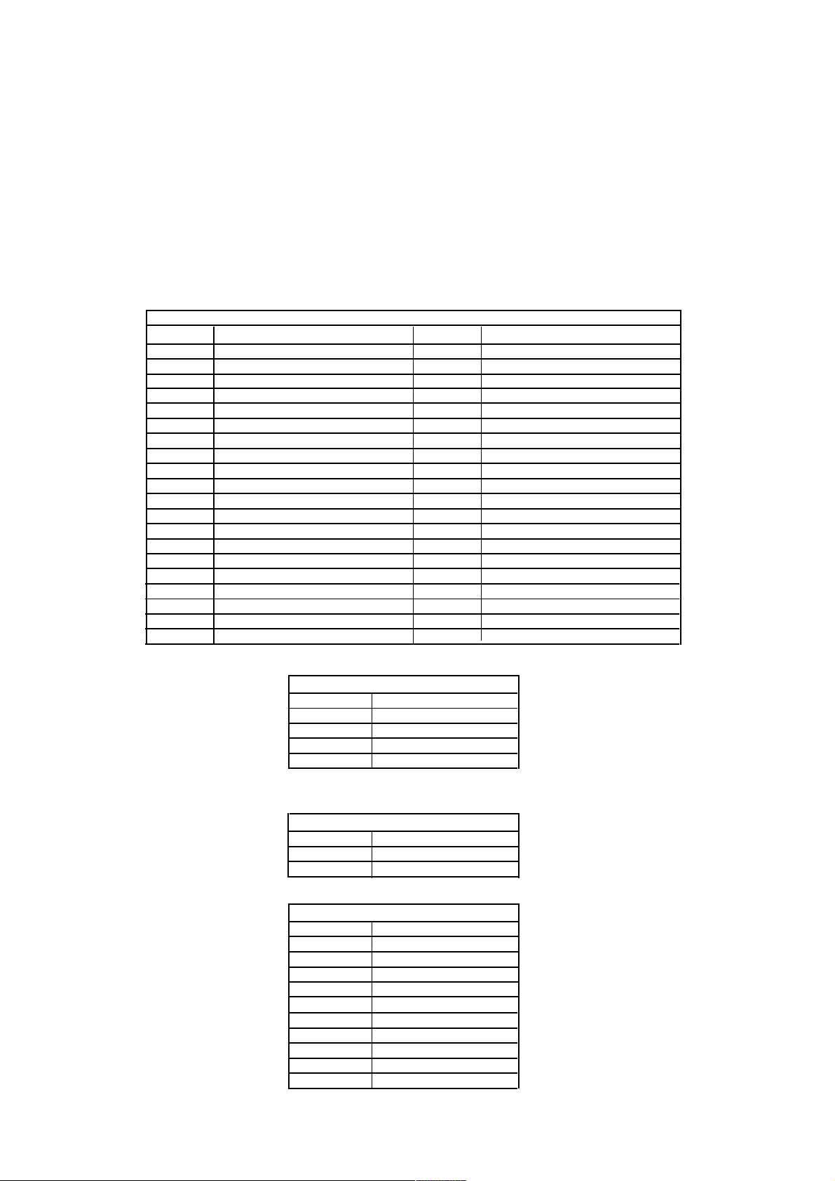
3 GPIO, IRQ, AND CHIP SELECT ASSIGNMENTS
PIO Port Bit Pin # STi5508 Alternate Function CineMaster CE Function
Port 0 Bit 0 186 SC0_DATA #SOFT_RESET
Port 0 Bit 1 187 #ATAPI_RD #ATAPI_RD
Port 0 Bit 2 188 #ATAPI_WR #ATAPI_WR
Port 0 Bit 3 189 SC0_CLK DAC_CCLK (Audio DAC control)
Port 0 Bit 4 190 SC0_RST DAC_CCLK (Audio DAC control)
Port 0 Bit 5 191 SC0_CMD_VCC #DAC_CS0 (Audio DAC control)
Port 0 Bit 6 192 SC0_DATA_DIR #DAC_CS1 (Audio DAC control)
Port 0 Bit 7 193 SC0_DETECT Unused (Test Point 39)
Port 1 Bit 0 194 SSC0_DATA SDA (I2C)
Port 1 Bit 1 195 SSC0_CLK SCL (I2C)
Port 1 Bit 2 196 PARA_DVALID/SC_EXT_CLK Unused (Test Point 35)
Port 1 Bit 3 197 TXD2 TXD (Serial Port)
Port 1 Bit 4 200 RXD2 RXD (Serial Port)
Port 1 Bit 5 201 PARA_SYNC/TXD1 SR0 (for PLL1700)
Port 1 Bit 6 202 TRIGIN TRIGIN (JTAG)
Port 1 Bit 7 203 TRIGOUT TRIGOUT (JTAG)
Port 2 Bit 0 204 SC1_DATA FPCLK (Front Panel)
Port 2 Bit 1 205 PARA_REQ/RXD1 FS0 (for PLL1700)
Port 2 Bit 2 206 PARA_STR FS1 (for PLL1700)
Port 2 Bit 3 207 SC1_CLK RTS (Serial Port)
Port 2 Bit 4 208 SC1_RST CTS (Serial Port)
Port 2 Bit 5 1 SC1_CMD_VCC FPDATA (Front Panel)
Port 2 Bit 6 2 DAC_DATA/SC1_DATA_DIR DAC_DATA (Stereo Audýo)
Port 2 Bit 7 3 SC1_DETECT FPSTRB (Front Panel)
4
Page 4

Port 3 Bit 0 6 PARA_DATA0 OPEN (TMM Tray Control)
Port 3 Bit 1 7 PARA_DATA1 CLOSE (TMM Tray Control)
Port 3 Bit 2 8 PARA_DATA2 Unused (Test Point 36)
Port 3 Bit 3 9 PARA_DATA3 Front Panel IR
Port 3 Bit 4 10 PARA_DATA4 Unused (Test Point 37)
Port 3 Bit 5 11 PARA_DATA5 Unused (Test Point 38)
Port 3 Bit 6 12 PARA_DATA6/COMP1 #SENSE (TMM Tray Control)
Port 3 Bit 7 13 PARA_DATA7/COMP2 #PUSH (TMM Tray Control)
Port 4 Bit 0 39 YUV0 YUV0 (External Video DENC)
Port 4 Bit 1 40 YUV1 YUV1
Port 4 Bit 2 41 YUV2 YUV2
Port 4 Bit 3 42 YUV3 YUV3
Port 4 Bit 4 43 YUV4 YUV4
Port 4 Bit 5 44 YUV5 YUV5
Port 4 Bit 6 45 YUV6 YUV6
Port 4 Bit 7 46 YUV7 YUV7
* Front Panel uses the 16311 controller. In the CineMaster design, FPDIN and FPDOUT are connected
together as FPDATA.
Pin Name Pin # STi5508 Pin Function CineMaster CE Function
#CE1 134 Programmable Chip Enable 1 ATAPI Buffer Chip Enable
#CE2 133 Programmable Chip Enable 2 Unused
#CE3 132 Programmable Chip Enable 3 FLASH Memory Chip Select
#IRQ0 127 Interrupt 1 Front Panel Interrupt
#IRQ1 126 Interrupt 2 Front End Interrupt (ATAPI/TMM)
#IRQ2 125 Interrupt 3 Unused
Table 1 GPIO, IRQ, and Chip Select Assignments
4. JUMPER CONFIGURATION
Jumper Function Installed Not Installed
JP1 Power +3.3V, +5V and +12V are Uninstalled all
Down disconnected from the components are powered
STi5508 and associated
circuitry using a FET switch
JP3 Boot From forces STi5508 to boot from Not Installed STi5508 will
Link JTAG interface only attempt to boot from
FLASH, but will also boot
from JTAG interface
* Note: There is no JP2
Table 2 Jumper Configuration
5. AUDIO OUTPUT
The STi5508 supports both a six channel analog output and a stereo output configuration. Both of these output configurations are available simultaneously (eight analog outputs total). In a system configuration with six analog outputs, the front
left and right channels can be configured to provide the stereo outputs, Dolby Surround, and SRS TruSurround, or the left
and right front channels for a 5.1 channel surround system.
The STi5508 also provides a stereo output channel that can be used in combination with the 5.1 outputs. An example of
this configuration is a DVD player with these stereo outputs connected to the TV and the six channel outputs connected
to the surround sound amplifier unit. In this setup, the consumer can use the TV speakers or the surround speaker
without changing any wires. The stereo output can be configured separately from the six-channel left and right outputs,
so, for example, the stereo output can be configured for Dolby ProLogic.
The Sti5508 also provides digital output in S/PDIF format. The evaluation board supports both optical and coaxial
S/PDIF outputs.
5.1 AUDIO DACs
The STi5508 supports several variations of an I²S type bus, varying the order of the data bits (leading or no leading zero
bit, left or right alignment within frame, and MSB or LSB first) is possible using the Sti5508 internal configuration registers.
The I²S format uses four stereo data lines and three clock lines. The I²S data and clock lines can be connected directly to
one or more audio DAC to generate analog audio output.
5
Page 5

The evaluation board uses a six-channel DAC and also a two-channel DAC. The six-channel DAC is connected to the
three STI5508 data signals for six-channel output and the two-channel DAC is connected to the STi5508 optional stereo
output. The board can be configured with either the six- or two-channel DAC, or both. When the two-channel DAC is not
used, the left and right front audio can be connected to the stereo audio output connectors by installing zero ohm resistors R364 and R365.
The six-channel DAC is an AKM AK4356. The two-channel DAC is an AK4394 also made by AKM. Both of these DACs
support up to 192Khz sampling rate. A less expensive 96kHz two-channel DAC with the same pin-out can be placed
instead of the AK4394. Four STi5508 PIO pins are used to configure the audio DACs. The outputs of the DACs are
differential, not single ended so a slightly more expensive buffering circuit is required. The buffer circuits use NJR
NJM5532 opamps to perform the low-pass filtering and the buffering.
5.2 AUDIO MUTE
The audio DACs contain an internal mute circuit and can be enabled by the STi5508 PIO pins. The evaluation board may
output a small pop when the system is powered on and off, but no audible pops should be heard during operation or
when entering or leaving standby mode.
6. VIDEO INTERFACE
The STi5508 integrates a PAL/NTSC encoder. It converts the digital MPEG/Sub Picture/OSD stream into a standard
analog baseband PAL/NTSC signals. Six analog video outputs provide CVBS, S-Video (Y/C), and RGB/YUV formats. The
three RGB signals can be configured via an internal STi5508 register setting to output either RGB or YUV video signals.
The encoder handles interlaced and non-interlaced mode. It can perform Closed Captions, CGMS or Teletext encoding
and allows Macrovision 7.01/6.1 copy protection. The encoder supports both master and slave modes for synchronization.
The six video signals are routed to the back panel where they are low-pass filtered and buffered. The six active video
buffer circuits on the decoder board are identical and use a video speed MAX4018 opamp made by Maxim.
The buffered CVBS video is available on a RCA (cinch) style jack, S-Video on a mini-DIN, RGB/YUV on a triple RCA
jack, and all six signals (and stereo audio) are available on a SCART connector.
Note:The STi5508 is not capable of placing the video synch information in the green signal as required by some RGB
monitors. The synch information must be obtained from the CVBS output and connected to the external sync input of an
RGB monitor.
Note:When the STi5508 is configured to output YUV signals, the RGB pins of the SCART connector will also output YUV.
6.1 SCART INTERFACE
The Ravisent evaluation board contains a SCART controller chip from ST Microelectronics, the STv6412. This controller
chip allows SCART daisy-chaining the SCART output from another device can be connected to the DVD player SCART
input and passed through when the DVD player is in standby.
All SCART functions are controlled by the 6412 chip, which is in turn controlled by the STi5508 over the I²C bus. Please
see the STv6412 AUDIO/VIDEO SWITCH MATRIX data sheet for more detailed information.
6.2 DIGITAL VIDEO INTERFACE
An external video DENC can be connected to the STi5508. The digital output and analog input headers are provided on the
board, J20 and J19 respectively. The video encoder is controlled via I2C through the header. Also supplied on the header
are +3.3V, +5V, ground, and +5V and 5V analog supplies. The output of the external DENC is then fed into the video
filter-buffers on board. The values of the discrete components in the filter-buffers should be changed to match the characteristics of the external DENC.
7. MPEG DECODER SDRAM MEMORY
The STi5508 includes glueless interfaces to SDRAM memory for the MPEG decoder. The STi5508 supports one or two
1Mx16bit chips or a 4Mx16bit SDRAM chip. However, the Ravisent evaluation board supports only a 64Mbit chip. The
device used is a 4M x 16 bit, 125MHz, 3.3V, 54 pin TSOP II, Micron Technology MCT48LC4M16A2TG-7 or equivalent.
8. PROCESSOR SDRAM MEMORY
The STi5508 supports DRAM or SDRAM on its processor bus without any glue logic required. The Ravisent evaluation
board supports only SDRAM - either a 1Mx16bit or a 4Mx16bit SDRAM. The STi5508 processor can be configured to
share the decoder memory. This will reduce performance slightly, but will reduce the cost of the system, as processor
SDRAM is no longer required. It is expected that a typical DVD player will not need any processor SDRAM and this chips
will only be installed for test and debug purposes.
Dual PCB footprints were used to accommodate the differences in packaging between 16M and 64M SDRAMS. U5/1 is
the 16Mbit footprint and U5/2 is the 64Mbit footprint. The same 64Mbit SDRAM used for decoder memory can be used for
processor SDRAM.
6
Page 6

9. FLASH MEMORY
The decoder board supports a single 1Mx16bit FLASH memory device. The device is a 1M x 16, 90ns, bottom boot block,
3.3V, 48 pin TSOP II, SGS Thomson M29F160BB-90N1 or equivalent. Both 3.3V and 5V FLASH devices can be installed.
Our current FLASH loading software supports several FLASH chips from different manufacturers. To support new chips, the
programming algorithm will have to be adapted, but this is a rather simple adaptation.
Note: Intel and Micron FLASH require that pins 13 and 14 are tied to the positive power supply to allow programming in
circuit. To support these device families, install zero ohm (0R0) resistors in locations R79 and R80.
Note: Install a zero ohm resistor in location R350 to support +5V FLASH. Install zero ohms in R352 to support +3.3V
FLASH. Never install both R350 and R352 at the same time as this will short the 3.3 and 5V supplies together. The default
is +3.3V.
Note: Some FLASH devices use pin 15 for address pin A19, while most others use pin 9. To support a chip that uses pin
15, install R81.
10. SERIAL EEPROM MEMORY
An I²C serial EEPROM is used to store user configuration (i.e. language preferences, speaker setup, etc.) and software
configuration information (i.e. remote control type). Industry standard EEPROM range in size from 1kbit to 256kbit and
share the same IC footprint and pinout. The default device is 2kbit, 256k x 8, SOIC8 SGS Thomson ST24C02M1 or
equivalent. See the section on Reset Circuitry for a less costly EEPROM solution.
11. TMM DRIVE INTERFACE
The STi5508 will directly supports a Thomson TVM502 drive (or a similar drive built around the ST chip drive set) without
any external glue logic. The newer TVM drives include the disc tray motor control circuitry, but the older drives do not.
Tray motor control circuitry is included on the evaluation board to support these older drives.
11.1 CONNECTION INFORMATION
The newer TMM drive uses a 19 pin FFC connector while the older drives use two PicoFlex ribbon connectors and a
two pin tray motor connector. Both connector systems are supported on the evaluation board. The drive interface, with
the exception of the tray motor circuitry, is contained entirely in the STi5508.
The older TMM drive connects to the evaluation board in three places:
J5 Drive tray motor terminals
J6 Power cable connector
J7 Data cable connector
The newer TMM drive connects to the evaluation board with a single connector:
J8 FFC19 connector
The connectors selected by Thomson for the data and power cables are in the PicoFlex product line manufactured by Molex
and Lumberg. The FFC connector is available from many suppliers including Molex. See Bill of Material for part numbers.
11.2 TMM DRIVE TRAY MOTOR CONTROL AND PUSH AND STALL SENSE CIRCUITRY
There is circuitry on the decoder board to power the TMM drive tray and to monitor its activity. When the tray is being
opened or closed and the tray has reached the end of its travel or is being jammed, the motor will stall and draw a high
current. Circuitry monitors the level of current used by the motor and will toggle a PIO pin of the STi5508 when the motor
has stalled, (schematic net name: #SENSE). The STi5508 will then remove power to the motor. Also, if the tray is open and
the user pushes the tray to close it, the motor will generate voltage. Circuitry will sense this voltage and toggle another PIO
pin, (schematic net name: #PUSH). The STi5508 will then close the tray.
The sensitivity of the push sense can be adjusted by changing the value of R114 in relation to R117. When the tray is
motionless, the voltage across the motor is zero. When the tray is pushed the voltages at either side of the motor begin to
diverge. These two voltages are fed into a comparator to create the trigger signal. This is an improved circuit from the
Ravisent STi5505 evaluation boards and this new circuit is not sensitive to temperature or component tolerances.
Note: To disable the push sense circuit, remove R109 and R112. R106 and R107 should already be installed.
12. ATAPI DRIVE INTERFACE AND EPLD
The STi5508 includes a glueless ATAPI interface on-chip. While this interface limits performance of the system, it is a lower
cost solution than providing external logic to interface the drive to the STi5508 front-end interface.
Standard ATAPI DVD drives are supported through the ATAPI EPLD interface. The drive connects to the decoder board
through a standard 40 pin header, The header is a 2 row by x 20 pins, 0.1 pin spacing, and has 0.025 square pins.
Note: The decoder board supports the standard ATAPI electrical connections, but the software protocol within the drive is
not always supported according to ATAPI specifications. Custom software may need to be developed and tested to support
ATAPI drives from different manufacturers.
7
Page 7

13 AUDIO SAMPLING RATE AND EXTERNAL PLL COMPONENT CONFIGURATION
The decoder board has optional PLLs, which can be installed to provide the audio clock for the system. The initial version
of the STi5505 was not able to provide an audio clock for 96kHz support and an external PLL was used to support this.
This was fixed in the STi5505 later chip revisions and therefore no problems are expected in the STi5508. However, in
case a problem arises, the PLL circuit can be installed to provide a high quality clock particularly important in S/PDIF
applications. In the default configuration, a small buffer chip is installed to buffer the audio clock between the STi5508
and the audio DACs.
14 UART SERIAL PORT
The evaluation board provides an RS232 connection to the STi5508. A standard DB9 connector ribbon cable can be
connected to the 10 pin header provided, (J9). The RS232 buffer can also be bypassed and the 3.3V signals can be
accessed on the header. ASC2 is the serial port used to this connection.
15. FRONT PANEL
15.1 FRONT PANEL MICRO
A Microchip PIC can be installed in the system to control the front panel VFD, perform IR remote control decoding and
power down functions, and read the position on two POTs with its internal ADC. When the front panel micro is installed,
the entire decoder board circuit can be powered down in standby mode because the PIC will decode the IR signals.
15.2 VFD CONTROLLER
The VFD controller is a NEC uPD16311. This controller is not a processor, but does include a simple state machine
which scans the VFD and reads the front panel button matrix. The 16311 also includes RAM so it can store the current
state of all the VFD icons and segments. Therefore, the 16311 need only be accessed when the VFD status changes
and when the button status is read. The STI5508 can control this chip directly using PIO pins or can allow the front panel
PIC to control the VFD.
15.3 MICROPHONE INPUTS
The board has two ¼ phono-jacks for microphone input. The microphone circuits consist of microphone pre-amps, a
signal buffers, and a stereo ADC. The microphone pre-amp, SSM2165, conditions the signal for better performance. The
stereo ADC is a Crystal CS5331 and connects directly to the STi5508 digital audio input via I²S.
Adjusting the value POT1 and POT2 can vary the compression characteristics of the microphone signal. See the
SSM2165 data sheet for a graph of the compression characteristics and POT settings. When the correct POT setting is
found, the pots can be replaced with fixed resistors, R382 and R383.
15.4 HEADPHONE OUTPUTS
The left and right audio is amplified and output through a stereo ¼ phono-jack. The audio is from the two-channel output,
not the let and right channel of the six-channel, (the left and right six-channel audio can be connected to the left and right
two-channel output when the stereo DAC is not installed). A dual logarithmic POT is used to adjust the volume of the
audio before amplification, POT5. The connections for left and right channels at the headphone jack can be swapped by
changing the resistor stuffing options, R376-379
.
16 MISCELLANEOUS FUNCTIONS
16.1 POWER DOWN
Two dual FET ICs can be installed on the decoder board to enable a power down feature. Power down is activated by
connecting a switch across JP1, shorting the two pins together pulling pin 2 to +5V. The front panel microcontroller can
also control the power down status by driving FPPWD high. When in power down state, power can be removed from all of
the circuitry except the front panel micro, which must remain power to decode remote control signaling and scanning the
front panel buttons. If the front panel micro is not used, then the STi5508 cannot be powered down.
The board can be configured in several ways to accomplish a power down goal. The net VCC_PIC is always powered.
VCC can either be switched (by installing R3) or always powered (by installing R1). VCC3 can either be switched (by
installing R5)or always powered (by installing R2). VCC-S, VCC3-S, +12V-S, and +8V-S are switched. There are four
LEDs used to indicate power state and they can be connected on either side of the FET switch. The dual FET is a
Fairchild NDS8934 and is located at Q1 and Q2.
Note: If the power down feature is enabled FPPWD must be driven by the front panel micro or some other source.
16.2 RESET CIRCUITRY
Three different chips are supported to provide the power-on-reset and pushbutton reset function: Analog Device ADM707
(or equivalent), Telcom Semiconductor TC1270, or Xicor X1242. The TC1270 is a lower cost alternative to the ADM707.
The Xicor device also includes 2kbits of Serial EEPROM storage and can be used to replace both the reset and
SEEPROM devices to reduce cost. All three devices support and pushbutton reset switch.
8
Page 8
16.3 VOLTAGE REGULATORS
There are two +5V linear regulators to generate +5V for the analog circuitry from +12V. A smaller DPAK surface mount
device can be used in most circumstances, but in applications were more than 150mA are required, a TO-220 throughhole package can be used.
The STi5508 requires 2.5V to operate. This voltage is generated from +5V.
Negative 5V is required by the audio buffer circuitry and this is generated in one of three ways. If 12V is supplied by the
power supply, it is regulated to 5V with a linear regulator. If no 12V is supplied, a DC-DC can be installed in U51 to
generate either 12V or 5V. The use of a switching regulator to generate the negative voltage may introduce noise into
that voltage, so better audio performance may be produced by generating 12V with the DC-DC converter and then
regulating this to 5V with a linear regulator.
17 CONNECTORS
17.1 ATAPI DRIVE STANDARD CONNECTOR
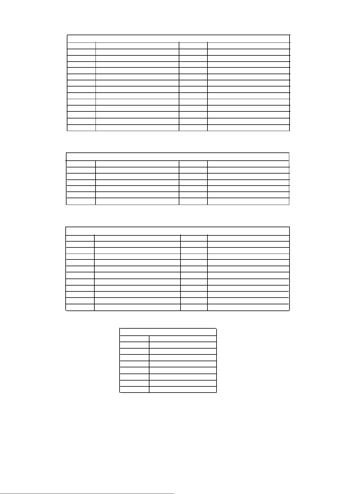
ATAPI Drive Interface J23
Pin Description Pin Description
1 #RESET 2 GND
3 DATA7 4 DATA8
5 DATA6 6 DATA9
7 DATA5 8 DATA10
9 DATA4 10 DATA11
11 DATA3 12 DATA12
13 DATA2 14 DATA13
15 DATA1 16 DATA14
17 DATA0 18 DATA15
19 GND 20 21 DMARQ 22 GND
23 #IOW 24 GND
25 #IOR 26 GND
27 IOCHRDY 28 GND
29 #DMACK 30 GND
31 INTRQ 32 HIO16
33 ADDR1 34 #PDIAG
35 ADDR0 36 ADDR2
37 #CS0 38 #CS1
39 - 40 GND
Table 3 ATAPI Drive Interface J23
17.2 TMM DRIVE CONNECTORS
TMM Tray Connector J5
Pin Description
1 +12V
2 GND
3 GND
4 +5V
Table 4 ATAPI Power Connector J4
TMM Tray Connector J5
Pin Description
1 OPEN
2 CLOSE
Table 5 TMM Tray Connector J5
TMM Power Connector J6
Pin Description
1 +5V (filtered)
2 +5V
3 GND
4 GND (filtered)
5 GND
6 +8V
7 GND
8 +12V
9 GND
10 +3.3V
Table 6 TMM Power Connector J6
9
Page 9

TMM Data Connector J7
Pin Description
2 GND
3 SYNC
4 FLAG
5 DATA
6 BCLK
7 GND
8 #FE RESET
9 FE I NT
10 SCL
11 SDA
12 GND
Table 7 TMM Data Connector J7
TMM FFC19 Connector J8
Pin Description Pin Description
1 - 11 SDA
2 GND 12 GND
3 SYNC 13 GND
4 FLAG 14 +3.3V
5 DATA 15 +5V
6 BCLK 16 GND
7 GND 17 GND (filtered)
8 #FRESET 18 +12V
9 FEINT 19 +8V or +12V
10 SCL
17.3 STI5508 JTAG INTERFACE
Pin Description Pin Description
1 - 2 GND
3 PIO3_7 4 GND
5 PIO3_6 6 GND
7 - 8 GND
9 TMS 10 GND
11 TCK 12 GND
13 TDI 14 GND
15 TDO 16 GND
17 #JTAG_RESET 18 GND
19 #TRST 20 GND
17.4 RS232 SERIAL PORT
Pin Description Pin Description
1 - 2 3 TXD 4 CTS
5 RXD 6 RTS
7 - 8 9 GND 10 -
Table 8 TMM FFC19 Connector J8
JTAG Programming Interface J2
Table 9 JTAG Programming Interface J2
RS232 Serial Port Header J9
Table 10 RS232 Serial Port Header J9
10
Page 10
17.5 DIGITAL YUV OUTPUT HEADER
Pin Description Pin Description
1 YUV0 2 GND
3 YUV1 4 GND
5 YUV2 6 GND
7 YUV3 8 VSYNC
9 YUV4 10 11 YUV5 12 HSYNC
13 YUV6 14 15 YUV7 16 GND
17 PIXCLK 18 GND
19 - 20 GND
21 SCL 22 +5V or +3.3V
23 SDA 24 +5V (analog)
25 GND 26 -5V (analog)
17.6 ANALOG VIDEO INPUT HEADER
Pin Description Pin Description
1 RED 2 GND
3 GREEN 4 GND
5 BLUE 6 GND
7 CHROMA 8 GND
9 LUMA 10 GND
11 CVBS 12 GND
17.7 SCART CONNECTORS
Digital YUV Output Header J20
Table 11 Digital YUV Output Header J20
Analog Video Input Header J19
Table 12 Analog Video Input Header J19
SCART Connectors J10
Pin Description Pin Description
1 RIGHT AUDIO OUT 2 RIGHT AUDIO IN
3 LEFT AUDIO OUT 4 GND
5 GND 6 LEFT AUDIO IN
7 BLUE 8 SWITCH
9 GND 10 11 GREEN 12 13 GND 14 GND
15 RED (CHROMA) 16 BLANK
17 GND 18 GND
19 CVBS OUT (LUMA) 20 CVBS IN
21 GND (shield)
Table 13 SCART Connectors J10
17.8 POWER CONNECTOR
Power Connector J1
Pin Description
1 +5 V
2 +3.3 V
3 +3.3 V
4 GND
5 GND
6 +12 V
1
7
1
8
GND
-12 V
Table 14 Power Connector J1
1
Connection to these two terminals is not required unless the board uses 12V. In a system without 12V,
a six pin header can be installed into pins one (1) through six (6) leaving pins seven (7) and eight (8) unpopulated.
18 SCHEMATICS
19 BILL OF MATERIALS
20 BOARD LAYOUT
20.1 TOP SIDE ASSEMBLY DRAWING
20.2 BOTTOM SIDE ASSEMBLY DRAWING
11
Page 11

CONTENTS
SAFETY PRECAUTIONS:................................................................................................................................................................2
• TV set switched off........................................................................................................................ 2
• Measurements ............................................................................................................................... 2
PERI-TV SOCKET..............................................................................................................................................................................2
• SCART 1......................................................................................................................................... 2
1. INTRODUCTION...........................................................................................................................................................................3
2. SMALL SIGNAL PART WITH STV2248.................................................................................... 3
• 2.1 Vision IF amplifier...................................................................................................................................................................3
• 2.2 QSS Sound circuit (QSS versions).......................................................................................................................................3
• 2.3 AM demodulator ...................................................................................................................................................................3
• 2.4 FM demodulator ....................................................................................................................................................................3
• 2.5 Video switch............................................................................................................................................................................4
• 2.6 Synchronisation circuit..........................................................................................................................................................4
• 2.7 Chroma and luminance processing......................................................................................................................................4
• 2.8 RGB output circuit..................................................................................................................................................................5
• 2.9 µ-Controller................................................................................................................................. 6
3. TUNER..............................................................................................................................................................................................6
5. SOUND OUTPUT STAGE TDA7496..........................................................................................................................................7
6. VERTICAL OUTPUT STAGE WITH TDA8174A....................................................................................................................7
7. VIDEO OUTPUT AMPLIFIER STV5114...................................................................................................................................7
8. POWER SUPPLY (SMPS) ............................................................................................................................................................7
10. SERIAL ACCESS CMOS 8K EEPROM 24C08.....................................................................................................................7
12. SAW FILTERS .............................................................................................................................................................................7
13. IC DESCRIPTIONS AND INTERNAL BLOCK DIAGRAM................................................................................................8
• ST92195.........................................................................................................................................................................................8
• STV224X.....................................................................................................................................................................................10
• UV1316, UV1336.........................................................................................................................................................................11
• TDA7496.....................................................................................................................................................................................12
• TDA8174.....................................................................................................................................................................................13
• STV5114......................................................................................................................................................................................13
• MC44608.....................................................................................................................................................................................14
• 24CO8..........................................................................................................................................................................................15
• SAW FILTERS...........................................................................................................................................................................16
GENERAL BLOCK DIAGRAM of 11AK46.................................................................................................................................17
Service menu ....................................................................................................................................................................................18
Options................................................................................................................................................................................................19
Languages..........................................................................................................................................................................................22
“1 1
Page 12

DO NOT CHANGE ANY MODULE UNLESS THE SET IS SWITCHED OFF
The mains supply part of the switch mode power supply’s transformer is live.
Use an isolating transformer.
The receiver complies with the safety requirements.
SAFETY PRECAUTIONS:
The service of this TV set must be carried out by qualified persons only. Components marked
with the warning symbol on the circuit diagram are critical for safety and must only be replaced with an
identical component.
- Power resistor and fused resistors must be mounted in an identical manner to the original component.
- When servicing this TV, check that the EHT does not exceed 26kV.
TV set switched off:
Make short-circuit between HV-CRT clip and CRT ground layer.
Short C809 before changing IC800 or other components in primary side of the SMPS part.
Measurements:
Voltage readings and oscilloscope traces are measured under the following conditions:
Antenna signal’s level is 60dB at the color bar pattern from the TV pattern generator. (100% white, 75%
color saturation)
Brightness, contrast, and color are adjusted for normal picture performance.
Mains supply, 220VAC, 50Hz.
PERI-TV SOCKET
- The figure of PERI-TV socket-
SCART 1 PINING
1 Audio right output 0.5Vrms / 1K
2 Audio right input 0.5Vrms / 10K
3 Audio left output 0.5Vrms / 1K
4 Ground AF
5 Ground Blue
6 Audio left input 0.5Vrms / 10K
7 Blue input 0.7Vpp / 75ohm
8 AV switching input 0-12VDC /10K
9 Ground Green
10 11 Green input 0.7Vpp / 75ohm
12 13 Ground Red
14 Ground Blanking
15 Red input 0.7Vpp / 75ohm
16 Blanking input 0-0.4VDC, 1-3VDC / 75 Ohm
17 Ground CVBS output
18 Ground CVBS input
“1 2
Page 13

19 CVBS output 1Vpp / 75ohm
20 CVBS input 1Vpp / 75ohm
21 Ground
1. INTRODUCTION
11AK46 is a 90° chassis capable of driving 14” tubes at the appropriate currents. The chassis is capable
of operating in PAL, SECAM and NTSC standards. The sound system is capable of giving 3,5 watt
RMS output into a load of 8 ohms. One page, 7 page SIMPLETEXT, TOPTEXT, FASTTEXT and US
Closed Caption is also provided. The chassis is equipped with a 42 pin Scart connector.
2. SMALL SIGNAL PART WITH STV2248:
STV2248 video processor is essential for realizing all small signal functions for a color TV receiver.
2.1 Vision IF amplifier3
The vision IF amplifier can demodulate signals with positive and negative modulation. The PLL
demodulator is completely alignment-free. Although the VCO (Toko-coil) of the PLL circuit is external,
yet the frequency is fixed to the required value by the original manufacturer thus the Toko-coil does not
need to be adjusted manually. The setting of the various frequencies (38.9 or 45.75 MHz) can be made
via changing the coil itself.
2.2 QSS Sound circuit (QSS versions)
The sound IF amplifier is similar to the vision IF amplifier and has an external AGC de-coupling capacitor.
The single reference QSS mixer is realised by a multiplier. In this multiplier the SIF signal is converted to
the inter-carrier frequency by mixing it with the regenerated picture carrier from the VCO. The mixer
output signal is supplied to the output via a high-pass filter for attenuation of the residual video signals.
With this system a high performance hi-fi stereo sound processing can be achieved. The AM sound
demodulator is realised by a multiplier. The modulated sound IF signal is multiplied in phase with the
limited SIF signal. The demodulator output signal is supplied to the output via a low-pass filter for
attenuation of the carrier harmonics. The AM signal is supplied to the output via the volume control.
2.3 AM DEMODULATOR
The AM demodulated signal results from multiplying the input signal by itself, it is available on
AM/FM output.
2.4 FM demodulator and audio amplifier :
The FM demodulator is realized as narrow-band PLL with external loop filter, which provides the
necessary selectivity without using an external band-pass filter. To obtain a good selectivity a linear phase
detector and constant input signal amplitude are required. For this reason the inter-carrier signal is
internally supplied to the demodulator via a gain controlled amplifier and AGC circuit. The nominal
frequency of the demodulator is tuned to the required frequency (4.5/5.5/6.0/6.5 MHz) by means of a
calibration circuit that uses the clock frequency of the µ-controller/Teletext decoder as a reference. The
setting to the wanted frequency is realized by means of the software. It can be read whether the PLL
frequency is inside or outside the window and whether the PLL is in lock or not. With this information it is
possible to make an automatic search system for the incoming sound frequency. This is realized by means
“1 3
Page 14

of a software loop that alternate the demodulator to various frequencies, then select the frequency on
which a lock condition has been found. De-emphasis output signal amplitude is independent of the TV
standard and has the same value for a frequency deviation of ±25 kHz at the 4.5 MHz standard and for a
deviation of ±50 kHz for the other standards. When the IF circuit is switched to positive modulation the
internal signal on de-emphasis pin is automatically muted. The audio control circuit contains an audio
switch and volume control. In the mono inter-carrier sound versions the Automatic Volume Leveling
(AVL) function can be activated. The pin to which the external capacitor has to be connected depends on
the IC version. For the 90° types the capacitor is connected to the EW output pin (pin 20). When the
AVL is active it automatically stabilizes the audio output signal to a certain level.
2.5 Video switching
The video processor (STV2248C) has three CVBS inputs and two RGB inputs. The first CVBS input is
used for external CVBS from SCART 1, the second is used for either CVBS or Y/C from BAV/FAV,
and the third one is used for internal video. The selection between both external video inputs signals is
realized by means of software and hardware switches.
2.6 Synchronization circuit
The video processor (STV224X) performs the horizontal and vertical processing. The external horizontal
deflection circuit is controlled via the Horizontal output pulse (HOUT). The vertical scanning is performed
through an external ramp generator and a vertical power amplifier IC controlled by the Vertical output
pulse (VOUT).
The main components of the deflection circuit are:
• PLL1: the first phase locked loop that locks the internal line frequency reference on the
CVBS input signal. It is composed of an integrated VCO (12 MHz) that requires the chroma
Reference frequency (4.43MHz or 3.58MHz crystal oscillator reference signal), a divider by
768, a line decoder, and a phase comparator.
• PLL2: The second phase locked loop that controls the phase of the horizontal output
(Compensation of horizontal deflection transistor storage time variation). Also the horizontal position
adjustment is also performed in PLL2.
• A vertical pulse extractor.
• A vertical countdown system to generate all vertical windows (vertical synchronization window, frame
blanking pulses, 50/60Hz identification window...).
• Automatic identification of 50/60Hz scanning.
• PLL1 time constant control.
• Noise detector, video identification circuits, and horizontal coincidence detector.
• Vertical output stage including de-interlace function, vertical position control.
• Vertical amplitude control voltage output (combined with chroma reference output and
Xtal 1 indication).
2.7 Chroma and luminance processing:
The chroma decoder is able to demodulate PAL, NTSC and SECAM signals.
The decoder dedicated to PAL and NTSC sub-carrier is based on a synchronous demodulator, and an
Xtal PLL locked on the phase reference signal (burst).
The SECAM demodulation is based on a PLL with automatic calibration loop.
The color standard identification is based on the burst recognition.
Automatic and forced modes can be selected through the I2C bus.
“1 4
Page 15

NTSC tint, and auto flesh are controlled through I2C bus.
Xtal PLL can handle up to 3 crystals to work in PAL M, PAL N and NTSC M for South America.
ACC an ACC overload control the chroma sub-carrier amplitude within 26dB range. Both
ACC s are based on digital systems and do not need external capacitor.
All chroma filters are fully integrated and tuned via a PLL locked on Xtal VCO signal.
A second PLL is used for accurate fine-tuning of the SECAM bell filter. This tuning is achieved during the
frame blanking. An external capacitor memorizes the bell filter tuning voltage.
A base-band chroma delay-line rebuilds the missing color line in SECAM and removes transmission
phase errors in PAL.
The base-band chroma delay line is clocked with 6MHz signal provided by the horizontal scanning VCO.
The luminance processor is composed of a chroma trap filter, a luminance delay line, a peaking function
with noise coring feature, a black stretch circuit.
Trap filter and luminance delay lines are achieved with the use of bi-quad integrated filters, auto-aligned
via a master filter phase locked loop.
2.8 RGB output circuit:
The video processor performs the R, G, B processing.
There are three sources:
1. Y,U,V inputs (coming from luma part (Y output), and chroma decoder outputs (R-Y, B-Y outputs).
2. External R,G,B inputs from SCART (converted internally in Y,U,V), with also the possibility to input
YUV signals from a DVD player, (YUV specification is Y=0.7 V PP , U= 0.7 V PP , V = 0.7V PP for
100% color bar).
3. Internal R,G,B inputs (for OSD and Teletext display)
The main functions of the video part are:
- Y,U,V inputs with integrated clamp loop, allowing a DC link with YUV outputs,
- External RGB inputs (RGB to YUV conversion), or direct YUV inputs,
- Y,U,V switches,
- Contrast, saturation, brightness controls,
- YUV to RGB matrix,
- OSD RGB input stages (with contrast control),
- RGB switches,
- APR function,
- DC adjustment of red and green channels,
- Drive adjustments (R, G, B gain),
- Digital automatic cut-off loop control,
- Manual cut-off capability with I2C adjustments,
- Half tone, oversize blanking, external insertion detection, blue screen,
- Blanking control and RGB output stages.
“1 5
Page 16

2.9 µ-Controller
The ST92195 is the micro-controller, which is required for a color TV receiver. ST92195D1 is the
version with one page Teletext and ST92195D7 is the one with 7 page Teletext. The IC has the supply
voltages of 5 V and they are mounted in PSDIP package with 56 pins.
µ-Controller has the following features
• Display of the program number, channel number, TV Standard, analogue values, sleep timer, parental
control and mute is done by OSD
• Single LED for standby and on mode indication
• System configuration with service mode
• 3 level logic output for SECAM and Tuner band switching
3. TUNER
PLL tuner is used as a tuner.
Channel coverage of UV1316:
BAND
OFF-AIR CHANNELS
CHANNELS FREQUENCY
RANGE (MHz)
CABLE CHANNELS
CHANNELS FREQUENCY
RANGE (MHz)
Low Band E2 to C 48.25 to 82.25 (1) S01 to S08 69.25 to 154.25
Mid Band E5 to E12 175.25 to 224.25 S09 to S38 161.25 to 439.25
High Band E21 to E69 471.25 to 855.25 (2) S39 to S41 447.25 to 463.25
(1). Enough margin is available to tune down to 45.25 MHz.
(2). Enough margin is available to tune up to 863.25 MHz.
Noise Typical Max. Gain Min. Typical Max.
Low band : 5dB 9dB All channels : 38dB 44dB 52dB
Mid band : 5dB 9dB Gain Taper (of-air channels): 8dB
High band : 6dB 9dB
“1 6
Page 17

Channel Coverage UV1336:
BAND CHANNELS FREQUENCY
RANGE (MHz)
Low Band 2 to D 55.25 to 139.25
Mid Band E to PP 145.25 to 391.25
High Band QQ to 69 397.25 to 801.25
Noise is typically 6dB for all channels. Gain is minimum 38dB and maximum 50dB for all channels.
5. SOUND OUTPUT STAGE TDA7496
TDA7496 is used as the AF output stereo amplifier . It is supplied by +20 VDC coming from a separate
winding in the SMPS transformer. An output power of 3.5W (THD=0.5%) can be delivered into an
8ohm load.
6. VERTICAL OUTPUT STAGE WITH TDA8174A
The TDA8174A is a power amplifier circuit for use in 90° and 110° colour deflection systems for 25 to
200 Hz field frequencies, and for 4: 3 and 16: 9 picture tubes.
7. VIDEO OUTPUT DISCRETE AMPLIFIERS
There are three monolithic video output amplifiers. Each amplifier consist of two transistors which are
TR_2SC2482 and BF421.
8. POWER SUPPLY (SMPS)
The DC voltages required at various parts of the chassis are provided by an SMPS transformer
controlled by the IC MC44608 which is designed for driving, controlling and protecting switching
transistor of SMPS. The transformer produces 115V for FBT input, ±14V for audio output IC, S+3.3,
S+5V and 8V for ST92195.
10. SERIAL ACCESS CMOS 8K EEPROM 24C08
The 24C08 is a 8Kbit electrically erasable programmable memory (EEPROM), organized as 4 blocks of
256*08 bits. The memory is compatible with the I²C standard, two wire serial interface which uses a bidirectional data bus and serial clock.
12. SAW FILTERS
Saw filter type: Model:
-66M: PAL SECAM B/G/D/K/I MONO
J1981 : PAL-I MONO
K2958M: PAL-SECAM B/G-D/K (38) MONO
L9653M: SECAM L/L’ AM MONO (AUDIO IF)
G3967M: PAL-SECAM B/G STEREO (VIDEO IF)
G9353M: PAL-SECAM B/G STEREO (AUDIO IF)
K3958M: PAL-SECAM B/G/D/K/I/L/L’ STEREO (VIDEO IF)
K9356M: PAL-SECAM B/G/D/K/I STEREO (AUDIO IF)
“1 7
Page 18

K9656M: PAL-SECAM B/G/D/K/I/L/L’ STEREO (AUDIO IF)
K3958M: PAL I NICAM (VIDEO IF)
K9356M: PAL I NICAM (AUDIO IF)
M1962M: PAL M/N NTSC M MONO
M3953M: PAL M/N NTSC M STEREO (VIDEO IF)
M9370M: PAL M/N NTSC M STEREO (AUDIO IF)
IC DESCRIPTIONS AND INTERNAL BLOCK DIAGRAM
• ST92195
• STV224X
• TUNER (UV1316, UV1336)
• TDA7496L
• TDA8174A
• STV5114
• MC44608
• 24C08
• SAW FILTERS
G1975M, K2966M, K2962M, L9653M, G3962M, G9353M, K3958M, K9356M, K9656M,
K6263K, K9652M,
M1962M, M3953M, M9370M
ST92195
The ST92195 is a member of the ST9+ family of micro-controllers, completely developed and produced
by SGS-THOMSON Microelectronics using a proprietary n-well HCMOS process. The nucleus of the
ST92195 is the advanced Core, which includes the Central Processing Unit (CPU), the ALU, the
Register File and the interrupt controller. The Core has independent memory and register buses to add to
the efficiency of the code. A set of on-chip peripherals form a complete sys-tem for TV set and VCR
applications:
– Voltage Synthesis
– VPS/WSS Slicer
– Teletext Slicer
– Teletext Display RAM
– OSD
Additional peripherals include a watchdog timer , a serial peripheral interface (SPI), a 16-bit timer and
an A/D converter.
“1 8
Page 19

“1 9
Page 20

STV224X Video processor:
The STV2246/2247/2248 are fully bus controlled ICs for TV including PIF, SIF, luma, Chroma and
deflection processing. Used with a vertical frame booster (TDA1771 or TDA8174 for 90° chassis,
STV9306 for 110° chassis), they allow the design of multi-standard (BGDKIMNLL, PAL/
SECAM/NTSC) sets with very few external components and no manual adjustments.
“1 10
Page 21

UV1316, UV1336
General description of UV1316:
The UV1316 tuner belongs to the UV 1300 family of tuners, which are designed to meet a wide range of
applications. It is a combined VHF, UHF tuner suitable for CCIR systems B/G, H, L, L’, I and I’.
Features of UV1316:
• Member of the UV1300 family small sized UHF/VHF tuners
• Systems CCIR: B/G, H, L, L’, I and I’; OIRT: D/K
• Digitally controlled (PLL) tuning via I²C-bus
• Off-air channels, S-cable channels and Hyper-band
• World standardized mechanical dimensions and world standard pinning
• Complies to “CENELEC EN55020” and “EN55013”
PINNING PIN VALUE
1. Gain control voltage (AGC) :4.0V, Max:4.5V
2. Tuning voltage
3. I²C-bus address select :Max:5.5V
4. I²C-bus serial clock :Min:-0.3V, Max:5.5V
5. I²C-bus serial data :Min:-0.3V, Max:5.5V
6. Not connected
7. PLL supply voltage :5.0V, Min:4.75V, Max:5.5V
8. ADC input
9. Tuner supply voltage :33V, Min:30V, Max:35V
10. Symmetrical IF output 1
11. Symmetrical IF output 2
General description of UV1336:
UV1336 series is developed for reception of channels broadcast in accordance with the M, N standard.
Features of UV1336:
• Global standard pinning
• Integrated Mixer-Oscillator & PLL function
• Conforms to CISPR 13, FCC and DOC (Canada) regulations
• Low power consumption
• Both Phono connector and ‘F’ connector are available
“1 11
Page 22

PINNING PIN VALUE
1. Gain control voltage :4.0V, Max:4.5V
2. Tuning voltage
3. Address select Max:5.5V
4. Serial clock :Min:-0.3V, Max:5.5V
5. Serial data :Min:-0.3V, Max:5.5V
6. Not connected
7. Supply voltage :5.0V, Min:4.75V, Max:5.5V
8. ADC input (optional)
9. Tuning supply voltage :33V, Min:30V, Max:35V
10. Ground
11. IF output
TDA7496
DESCRIPTION
The TDA7496 is a stereo 5+5W class AB power amplifier assembled in the @ Multiwatt 15 pack-age,
specially designed for high quality sound, TV applications. Features of the TDA7496 include linear
volume control, Stand-by and mute functions.
-5+5W OUTPUT POWER
-RL =?W@THD= 10% VCC = 22V
-ST-BY AND MUTE FUNCTIONS
-LOW TURN-ON TURN-OFF POP NOISE
-LINEAR VOLUME CONTROL DC COUPLED
-WITH POWEROP. AMP.
-NO BOUCHEROT CELL
-NO ST-BY RC INPUT NETWORK
-SINGLE SUPPLY RANGING UP TO 35V
-SHORT CIRCUIT PROTECTION
-THERMAL OVERLOAD PROTECTION
-INTERNALLY FIXED GAIN
-SOFT CLIPPING
-VARIABLE OUTPUT AFTER VOLUME CON-TROL
-CIRCUIT
-MULTIWATT 15 PACKAGE
PINNING
1 INR.
2 VAROUT_R
3 VOLUME
4 VAROUT_L
5 INL
6 NC
“1 12
Page 23

7 SWR
8 S_GNR
9 STBY
10 MUTE
11 PW_GND
12 OUTL
13 VS
14 OUTR
15 PW1_GND
TDA8174AW
Independent vertical amplitude adjustement. buffer stage. Power amplifier flyback generator thermal
protection . Internal reference voltage decou-pling
General Description:
TDA8174A and TDA8174AWare a monolithic integrated circuits. It is a full performance and very
efficient vertical deflection circuit intended for direct drive of a TV picture tube in Color and B & W
television as well as in Monitor and Data displays.
PINNING
1. POWER OUTPUT
2. OUTPUT STAGE Vs
3. TRIGGER INPUT
4. HEIGHT ADJUSTMENT
5. VOLTAGE REF DECOUPLING
6. GROUND
7. RAMP GENERATOR
8. BUFFER OUTPUT
9. INVERTING INPUT
10. Vs
11. FLYBACK GENERATOR
STV5114
25MHz BANDWIDTH
CROSSTALK : 55dB
SHORT CIRCUIT TO GROUND OR VCC PRO-TECTED
ANTI SATURATION GAIN CHANGING
VIDEO SWITCHING
“1 13
Page 24

DESCRIPTION
This integrated circuit provides RGB switching al-lowing connections between peri TV plug, internal RGB
generator and video processor in a TV set. The input signal black level is tied to the same reference
voltageon each input in order to have no differential voltage when switching two RGB generators.
An AC output signal higher than 2 Vpp makes gain going slowly down to 0dBto protect the TV set video
amplifier from saturation. Fast blanking output is a logicial OR between FB1
(Pin 8) and FB2 (Pin 10).
PINNING PIN VALUE
1. R1IN
2. GND
3. R2IN
4. G1IN
5. G2IN
6. B1IN
7. B2IN
8. FB1IN
9. FBOUT
10. FB2+FBBIN
11. BOUT
12. FBGIN
13. GOUT
14. VCC
15. FBRIN
16. ROUT
MC44608
General description:
The MC44608 is a high performance voltage-mode controller designed for off–line converters. This high
voltage circuit that integrates the start–up current source and the oscillator capacitor, requires few external
components while offering a high flexibility and reliability.
The device also features a very high efficiency stand–by management consisting of an effective Pulsed
Mode operation. This technique enables the reduction of the stand–by power consumption to
approximately 1W while delivering 300mW in a 150W SMPS.
• Integrated start–up current source
• Loss less off–line start–up
• Direct off–line operation
• Fast start–up
General Features
• Flexibility
• Duty cycle control
“1 14
Page 25

• On chip oscillator switching frequency 40, or 75kHz
• Secondary control with few external components
Protections
• Maximum duty cycle limitation
• Cycle by cycle current limitation
• Demagnetization (Zero current detection) protection
• “Over V CC protection” against open loop
• Programmable low inertia over voltage protection against open loop
• Internal thermal protection
GreenLine Controller
• Pulsed mode techniques for a very high efficiency low power mode
• Lossless startup
• Low dV/dT for low EMI radiations
PINNING PIN VALUE
1. Demagnetization Zero cross detection voltage: 50 mV typ.
2. I Sense Over current protection voltage 1V typ.
3. Control Input Min: 7.5V Max.: 18V
4. Ground Iout 2A
5. Driver Output resistor 8.5 Ohm sink 15 Ohm source typ.
6. Supply voltage Max:16V (Operating range 6.6V-13V)
7. No connection
8. Line Voltage Min:50V Max:500V
during scan 1.2A
p-p
during flyback
p-p
24CO8
General description:
The 24C16 is a 8Kbit electrically erasable programmable memory (EEPROM), organized as 4 blocks of
256 * 08 bits. The memory operates with a power supply value as low as 2.5V.
Features:
• Minimum 1 million ERASE/WRITE cycles with over 10 years data retention
• Single supply voltage:4.5 to 5.5V
• Two wire serial interface, fully I²C-bus compatible
• Byte and Multi-byte write (up to 8 bytes)
• Page write (up to 16 bytes)
• Byte, random and sequential read modes
• Self timed programming cycle
PINNING PIN VALUE
1. Write protect enable :0V
2. Not connected :0V
3. Chip enable input :0V
4. Ground :0V
5. Serial data address input/output :Input LOW voltage: Min:-0.3V, Max:0.3*Vcc
:Input HIGH voltage: Min:0.7*Vcc, Max:Vcc+1
6. Serial clock :Input LOW voltage: Min:-0.3V, Max:0.3*Vcc
:Input HIGH voltage: Min:0.7*Vcc, Max:Vcc+1
“1 15
Page 26

7. Multibyte/Page write mode :Input LOW voltage: Min:-0.3V, Max:0.5V
VIDEO
AUDIO
PAL BG
G1975M
PSBG DK
K2966M
PAL II'
J1981
PSBGDKK' II'
K2966M
PSBGDKK' LL'
K2962M
L9653
VIDEO
AUDIO
PAL BG
G3967M
G9353M
PAL II'
K3958M
K9356
PSBGDKK' II'
K3958M
K9356
PSBGDKK' LL'
K3958M
K9656
:Input HIGH voltage: Min:Vcc-0.5, Max:Vcc+1
8. Supply voltage :Min:2.5V, Max:5.5V
Saw filter’s list:
MONOSTR
PINNING
1. Input
2. Input-ground
3. Chip carrier-ground
4. Output
5. Output
K9656M, L9653M
PINNING
1. Input
2. Switching Input
3. Chip carrier-ground
4. Output
5. Output
“1 16
Page 27

“1 17
Page 28

Page 29

DVD MODULE
PLL TUNER
UV1316
2
I
C
SERVICE
GENERAL BLOCK DIAGRAM of 11AK46
SCART F-AV
AUDIO SWITCHING
R L
CIRCUITS
R
MONO
TDA7496
AU.
AMP
RGB
AMP
NVM
IF
ST92195
KEYPAD
MICRO
CONTROLLER
IR SENSOR
SMPS
MC
44608
115V
+12V AUD.
+8V
+5V
SWITCHING CIRCUITS
+5V St-by
“1 19
VIDEO
STV2248C
VIDEO
PROCESSOR
VER
AMP
TDA8174AW
HORIZONTAL
DRIVE
BU808DF
FBT
Page 30

DVD SCART1 FAV/BAV SVHS
SUPPLY
DVD POWER
“1 20
Page 31

SIRANOREGISTER PARAMETER
1 OSD OSD Horizontal Position
2 IF1 IF Coarse Adjust
3 IF2 IF Fine Adjust
4 IF3 IF Coarse Adjust for L-Prime
5 IF4 IF Fine Adjust for L-Prime
6 AGC Automatic Gain Control
7 VLIN Vertical Linearity
8 VS1A Vertical Size for 50 Hz / 4:3
9 VS1B Vertical Size for 50 Hz / 16:9
10 VP1 Vertical Position for 50 Hz
11 HP1 Horizontal Position for 50 Hz
12 VS2A Vertical Size for 60 Hz / 4:3
13 VS2B Vertical Size for 60 Hz / 16:9
14 VP2 Vertical Position for 60 Hz
15 HP2 Horizontal Position for 60 Hz
16 RGBH RGB Horizontal Shift Offset
17 WR White Point Adjust for RED
18 WG White Point Adjust for GREEN
19 WB White Point Adjust for BLUE
20 BR Bias for RED
21 BG Bias for GREEN
22 APR APR Threshold
23 FMP1 FM Prescaler when AVL is OFF
24 NIP1 NICAM Prescaler when AVL is OFF
25 SCP1 SCART Prescaler when AVL is OFF
26 FMP2 FM Prescaler when AVL is ON
27 NIP2 NICAM Prescaler when AVL is ON
28 SCP2 SCART Prescaler when AVL is ON
29 F1H High Byte of crossover frequency for VHF1-VHF3
30 F1L Low Byte of crossover frequency for VHF1-VHF3
31 F2H High Byte of crossover frequency for VHF3-UHF
32 F2L Low Byte of crossover frequency for VHF3-UHF
33 BS1 Band Switch Byte for VHF1 Meaningful for only
34 BS2 Band Switch Byte for VHF3 Meaningful for only
35 BS3 Band Switch Byte for UHF Meaningful for only
36 CB Control Byte Meaningful for only PLL Tuner
37 OP1 Option 1 (see the Option List)
38 OP2 Option 2 (see the Option List)
39 OP3 Option 3 (see the Option List)
40 OP4 Option 4 (see the Option List)
41 OP5 Option 5 (see the Option List)
42 TX1 Teletext Option 1 (see the Option List)
“1 21
Page 32

OP1 – Peripheral Options
BIT-7 NOT USED
BIT-6 1, Display “AV-3” as “F-AV”
0, Display “AV-3” as “B-AV”
BIT-5 1, Turn back TV mode after the last AV (with AV key)
0, Turn back first AV mode after the last AV
BIT-4 1, SVHS is available in AV key stream
0, SVHS is NOT available in AV key stream
BIT-3 1, RGB is available in AV key stream
0, RGB is NOT available in AV key stream
BIT-2 1, AV-3 is available in AV key stream
0, AV-3 is NOT available in AV key stream
BIT-1 1, DVD is available in AV key stream
0, DVD is NOT available in AV key stream
BIT-0 1, AV-1 is available in AV key stream
0, AV-1 is NOT available in AV key stream
OP2 – Reception Standard Options
BIT-7 1, 3-button keyboard (V-, P+, V+)
0, 4/5 button keyboard (V-, V+, P-, P+, Menu)
BIT-6 1, L/L’ is available
0, L/L’ is not available
BIT-5 1, I is available
0, I is not available
BIT-4 1, DK is available
0, DK is not available
BIT-3 1, BG is available
0, BG is not available
BIT-2 RESERVED (Keep as "0")
BIT-1 RESERVED (Keep as "0")
BIT-0 1, WFI available
0, WFI NOT available
OP3 – Video Options
BIT-7 Xtal Configuration
BIT-6 00, 1 Xtal PAL 4.43
01, 2 Xtal PAL/NTSC 4.43/3.58
10, 1 Xtal PAL/SEC/NTSC 4.43
11, 2 Xtal PAL/SEC/NTSC 4.43/3.58
BIT-5 1, Enable Blue back when no signal in AV modes
0, No Blue back in AV modes
BIT-4 1, White Insertion is ON
0, White Insertion is OFF
BIT-3 1, Blue Background when no signal
0, Disable Blue Background
BIT-2 1, Semi-transparent background for menu
0, Solid Menu background for menu
“1 22
Page 33

BIT-1 1, Black Stretch is ON
0, Black Stretch is OFF
BIT-0 1, APR is ON
0, APR is OFF
OP4 – TV Features
BIT-7 1, Headphone is available (for STEREO models)
0, Headphone is not available
BIT-6 1, Arabic/Persian ON
0, Arabic/Persian OFF
BIT-5 1, Hebrew ON
0, Hebrew OFF
BIT-4 1, Hotel Mode can be activated
0, Hotel Mode can not be activated
BIT-3 1, No Signal Timer is enabled
0, No Signal Timer is disabled
BIT-2
For PLL Tuner
1, Frequency based search
0, Channel table based search
For VST Tuner
1, VST Band drive is negative logic (with transistors on the chassis)
0, VST Band drive is positive logic (without transistors on the chassis)
BIT-1 1, 3-band tuning (VHF1, VHF3, UHF)
0, 1-band tuning (only UHF)
BIT-0 1, Extra 200 msec blanking for VST
0, no-extra blanking
OP5 – Channel Tables
BIT-7 1, Extra 150 msec blanking more for VST
0, no-extra blanking
BIT-6 1, “Programme” item in AUTOSTORE menu is visible
0, “Programme” item in AUTOSTORE menu is invisible
BIT-5 NOT USED
BIT-4 1, French OS Channel Table is available
0, French OS Channel Table is not available
BIT-3 1, French Channel Table is available
0, French Channel Table is not available
BIT-2 1, England Channel Table is available
0, England Channel Table is not available
BIT-1 1, East Europe Channel Table is available
0, East Europe Channel Table is not available
BIT-0 1, West Europe Channel Table is available
0, West Europe Channel Table is not available
TX1 – Teletext Options
BIT-7 NOT USED
BIT-6 RESERVED (must be 0)
“1 23
Page 34

BIT-5
BIT-4
BIT-3
BIT-2 2 1 0 Device type selection
BIT-1 000, EPROM M6 A
BIT-0 001, ROM H5 P
5 4 3 Teletext Language Groups
000, Group 1 – West
(English, French, Swedish, Czech, German, Portuguese, Italien, Rumanian)
001, Group 2 – West/East
(Polish, French, Swedish, Czech, German, Serbian, Italien, Rumanian)
010, Group 3 – West/Turkish
(English, French, Swedish, Turkish, German, Portuguese, Italien, Rumanian)
011, Group 4 – East/Cyrillic
(English, Cyrillic, Swedish, Czech, German, Serbian, Lettish, Rumanian)
100, Group 5 – Arabic
(English, French, Swedish, Turkish, German, Hebrew, Italien, Arabic)
010, ROMLESS H5 P
011, EPROM M6 R
100, ROM M6 R
101, OSDEPROM M6 R
110, ROM M6 P
111, Read Auto Gain Table for the device from EEPROM
AK46/TITANIUM – Languages Groups
GROUP 1 - WEST
• ENGLISH
• FRENCH
• SWEDISH
• CZECH
• GERMAN
• PORTUGUESE
• ITALIAN
• RUMANIAN
GROUP 2 – WEST / EAST
• POLISH
• FRENCH
• SWEDISH
• CZECH
• GERMAN
• SERBIAN
• ITALIAN
• RUMANIAN
• GROUP 3 – WEST / TURKEY
• ENGLISH
• FRENCH
• SWEDISH
• TURKISH
• GERMAN
• PORTUGUESE
• ITALIAN
• RUMANIAN
GROUP 4 – EAST / CYRILLIC
• ENGLISH
• CYRILLIC
• SWEDISH
“1 24
Page 35

• CZECH
• GERMAN
• SERBIAN
• LETTISH
• RUMANIAN
GROUP 5 - ARABIC
• ENGLISH
• FRENCH
• SWEDISH
• TURKISH
• GERMAN
• HEBREW
• ITALIAN
• ARABIC
Using Coloured Buttons
RED : No function.
GREEN : Is used to switch the aspect ratio between 4:3 and 16:9.
YELLOW : Is used to prepare the system for screen-adjustments.
BLUE : No function.
“1 25
Page 36

Page 37

Page 38

Page 39

Page 40

Page 41

 Loading...