SANYO VPC-E6U, VPC-E6GXW, VPC-E6GX, VPC-E6EXW, VPC-E6EX WARNING
...
WARNING
Do not use solder containing lead.
This product has been manufactured using lead-free solder in
order to help preserve the environment.
Because of this, be sure to use lead-free solder when carrying
out repair work, and never use solder containing lead.
Lead-free solder has a melting point that is 30 - 40°C (86 104°F) higher than solder containing lead, and moreover it does
not contain lead which attaches easily to other metals. As a
result, it does not melt as easily as solder containing lead, and
soldering will be more difficult even if the temperature of the
soldering iron is increased.
The extra difficulty in soldering means that soldering time will
increase and damage to the components or the circuit board
may easily occur.
Because of this, you should use a soldering iron and solder
that satisfy the following conditions when carrying out repair
work.
Soldering iron
Use a soldering iron which is 70 W or equivalent, and which
lets you adjust the tip temperature up to 450°C (842°F). It
should also have as good temperature recovery characteristics as possible.
Set the temperature to 350°C (662°F) or less for chip components, to 380°C (716°F) for lead wires and similar, and to 420°C
(788°F) when installing and removing shield plates.
The tip of the soldering iron should have a C-cut shape or a
driver shape so that it can contact the circuit board as flat or in
a line as much as possible.
Note:
If replacing existing solder containing lead with lead-free solder in the soldered parts of products that have been manufactured up until now, remove all of the existing solder at those
parts before applying the lead-free solder.
Solder
Use solder with the metal content and composition ratio by
weight given in the table below. Do not use solders which do
not meet these conditions.
Metal content
Composition
ratio by weight
Lead-free solder is available for purchase as a service tool.
Use the following part number when ordering:
Part name: Lead-free solder with resin (0.5 mm dia., 500 g)
Part number: VJ8-0270
Tin (Sn) Silver (Ag)
96.5 %
3.0 %
Copper (Cu)
0.5 %
– 2 –

1. OUTLINE OF CIRCUIT DESCRIPTION
1-1. CCD CIRCUIT DESCRIPTION
1. IC Configuration
The CCD peripheral circuit block basically consists of the following ICs.
IC903 (MN39830PLJ-A) CCD imager
IC901 (AN20112A) V driver
IC905 (AD9996BBCZ) CDS, AGC, A/D converter,
H driver, vertical TG
Pin 1
5
V
6
12
Pin 13
H
58
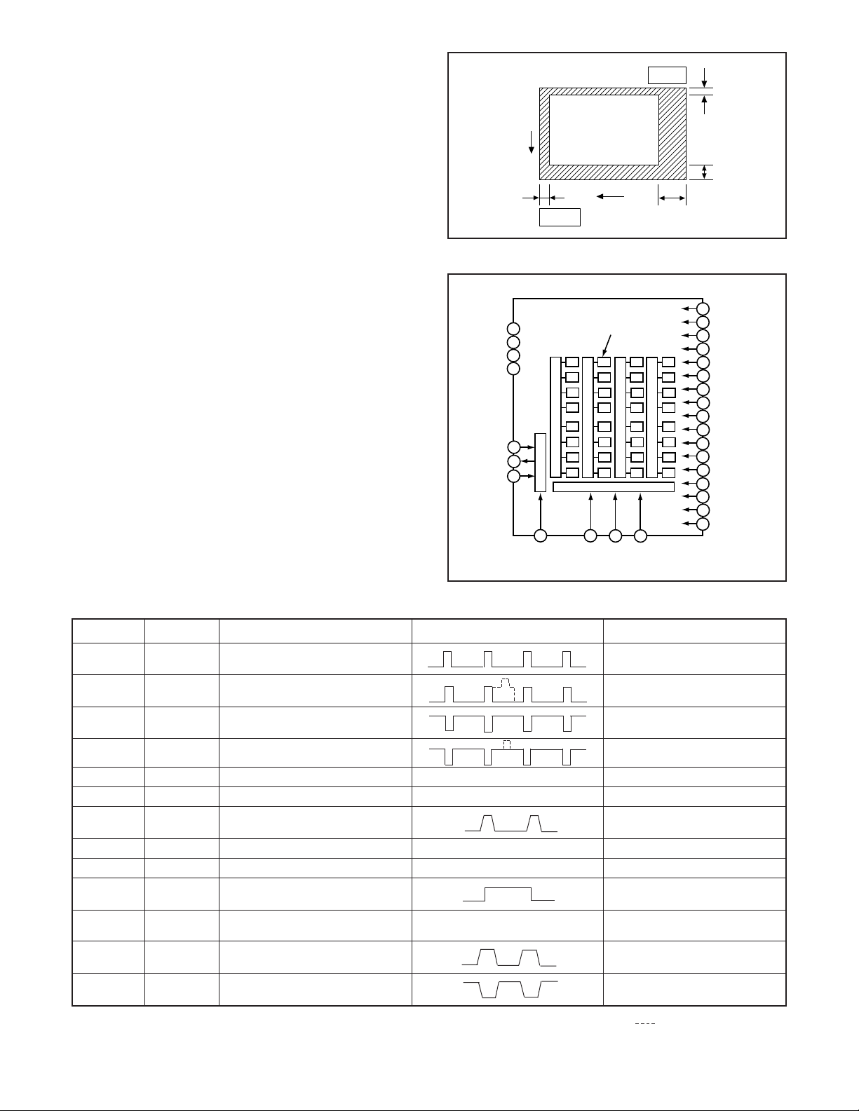
2. IC903 (CCD)
[Structure]
Interline type CCD image sensor
Optical size 1/2.5 type format
Effective pixels 2864 (H) X 2160 (V)
Pixels in total 2934 (H) X 2171 (V)
Optical black
Horizontal (H) direction: Front 12 pixels, Rear 58 pixels
Vertical (V) direction: Front 6 pixels, Rear 5 pixels
Dummy bit number Horizontal : 28 Vertical :7
Pin No.
Symbol Pin Description
Fig. 1-1.Optical Black Location (Top View)
NC
NC
NC
NC
VDD
VO
GND
13
14
27
28
15
16
17
18
Photo diode
Vertical shift register
Output part
Horizontal shift register
22
RG
ø
HL
ø
10
11
12
25
26
19
20
23
24
H2
H1
ø
ø
21
Fig. 1-2. CCD Block Diagram
Waveform
Voltag e
ø
1
ø
2
ø
3
ø
4
ø
5
ø
6
ø
7
ø
8
9
ø
ø
ø
GND
ø
ø
PT
SUBSW
ø
V6
V5B
V5A
V4
V3B
V3A
V3L
V3R
V2
V1
V1S
V5R
V5L
Vsub
1, 25, 26
2, 3
4, 7, 8, 9, 11
5, 6, 10
16
15
18
12, 17
19
20
21
22, 23
24
5L, V5R, V6
V
5A, V5B Vertical register transfer clock
V
V1S, V2, V3L,
V3R, V4
V
1, V3A, V3B
VO
VDD
ØRG
GND
PT
Vertical register transfer clock
Vertical register transfer clock
Vertical register transfer clock
Signal output
Circuit power DC 12 V
Reset gate clock
GND
Protection transister bias
Substrate controlSUB SW
SUB
L, H1
H
H
Substrate clock
Horizontal register transfer clock
Horizontal register transfer clock
2
Table 1-1. CCD Pin Description
-6.0 V, 0 V
-6.0 V, 0 V, 12 V
-6.0 V, 0 V
-6.0 V, 0 V, 12 V
DC
Aprox. 12 V
4.5 V, 7.8 V
GND 0 V
DC
-6.0 V
0, 3.3 V (When importing all
picture element: 3.3 V)
DC
Aprox. 6 V
(Different from every CCD)
0 V, 3.3 V
0 V, 3.3 V
When sensor read-out
– 3 –

3. Part of IC905 (generation of vertical transfer clock,
H Driver) and IC901 (V Driver)
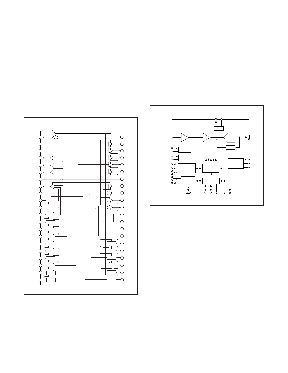
An H driver (part of IC905) and V driver (IC901) are necessary in order to generate the clocks (vertical transfer clock,
horizontal transfer clock and electronic shutter clock) which
driver the CCD.
IC905 has the generation of horizontal transfer clock and the
function of H driver, and is an inverter IC which drives the
horizontal CCDs (H1 and H2). It carries out generating vertical transfer clock, and output to IC901.
In addition the XV1-XV6 signals which are output from IC905
are vertical transfer clocks, and the XSG signal is superimposed onto XV1, XV3 and XV5 at IC901 in order to generate
a ternary pulse. In addition, the XSUB signal which is output
from IC101 is used as the sweep pulse for the electronic shutter, and the RG signal which is output from IC905 is the reset
gate clock.
4. IC905 (H Driver, CDS, AGC and A/D converter)
IC905 contains the functions of H driver, CDS, AGC and A/D
converter. As horizontal clock driver for CCD image sensor,
HØ1 (A and B) and HØ2 (A and B) are generated inside, and
output to CCD.
The video signal which is output from the CCD is input to pin
(A6) of IC905. There are sampling hold blocks generated from
the SHP and SHD pulses, and it is here that CDS (correlated
double sampling) is carried out.
After passing through the CDS circuit, the signal passes
through the AGC amplifier (VGA: Variable Gain Amplifier). It
is A/D converted internally into a 14-bit signal, and is then
input to ASIC (IC101). The gain of the VGA amplifier is controlled by pin (A2), (B3) and (C4) serial signal which is output
from ASIC (IC101).
REFB
REFT
OSUB
VM
OV1
RESET
SUBCNT
VDC
CH1
V5R
V5L
V3R
V3L
V1S
CLI
AD9996
14-BIT
ADC
CLAMP
INTERNAL
REGISTERS
CLO
14
DOUT
SL
SCK
SDI
VMSUB
9
3-level
10
VL
5
VL
27
2-level
24OV2
2-level
23OV4
2-level
21OV6
8
3-level
20
28
Level
1
conversion
3
Level
32
conversion
Level
V1
33
conversion
Level
31
V6
conversion
Level
V4
30
conversion
Level
29
V2
conversion
Level
37
conversion
Level
38
conversion
Level
35
conversion
Level
36
conversion
Level
34
conversion
2-level
2-level
2-level
2-level
2-level
3-level
3-level
3-level
3-level
Level
conversion
Level
conversion
Level
conversion
Level
conversion
Level
conversion
Level
conversion
Level
conversion
7
VHH
16
OV5R
15
OV5L
18
OV3R
17
OV3L
19
OV1S
25
VM
12
OV5A
11
OV5B
14
OV3A
13
OV3B
6
VH
26
VH
4
GND
41
CH2
40
V3
39
CH4
44
CH3
43
V5
42
CH5
2
SUB
CCDIN
3V INPUT
1.8V OUTPUT
1.8V INPUT
3V OUTPUT
H1 TO H8
XV1 TO XV24
XSUBCK
RG
HL
CDS
-3dB, 0dB, +3dB
LDO
REG
CHARGE
PUMP
HORIZONTAL
DRIVERS
8
24
VERTICAL
TIMING
CONTROL
8
GP01 TO GP08
Fig. 1-4. IC905 Block Diagram
6~42 dB
VGA
INTERNAL
CLOCKS
PRECISION
TIMING
GENERATOR
SYNC
GENERATOR
VD
HD
SYNC
VREF
Fig. 1-3. IC901 Block Diagram
– 4 –
 Loading...