

Page 1
1. OUTLINE OF CIRCUIT DESCRIPTION
1-1. CCD CIRCUIT DESCRIPTION
1. IC Configuration
The CCD peripheral circuit block basically consists of the following ICs.
IC903 (MN39830PLJ-A) CCD imager
IC901 (AN20112A) V driver
IC905 (AD9996BBCZ) CDS, AGC, A/D converter,
H driver, vertical TG
Pin 1
5
V
6
12
Pin 13
H
58
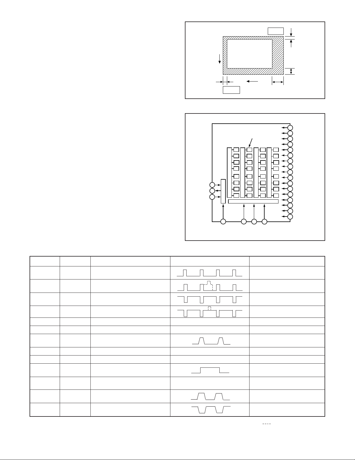
2. IC903 (CCD)
[Structure]
Interline type CCD image sensor
Optical size 1/2.5 type format
Effective pixels 2864 (H) X 2160 (V)
Pixels in total 2934 (H) X 2171 (V)
Optical black
Horizontal (H) direction: Front 12 pixels, Rear 58 pixels
Vertical (V) direction: Front 6 pixels, Rear 5 pixels
Dummy bit number Horizontal : 28 Vertical :7
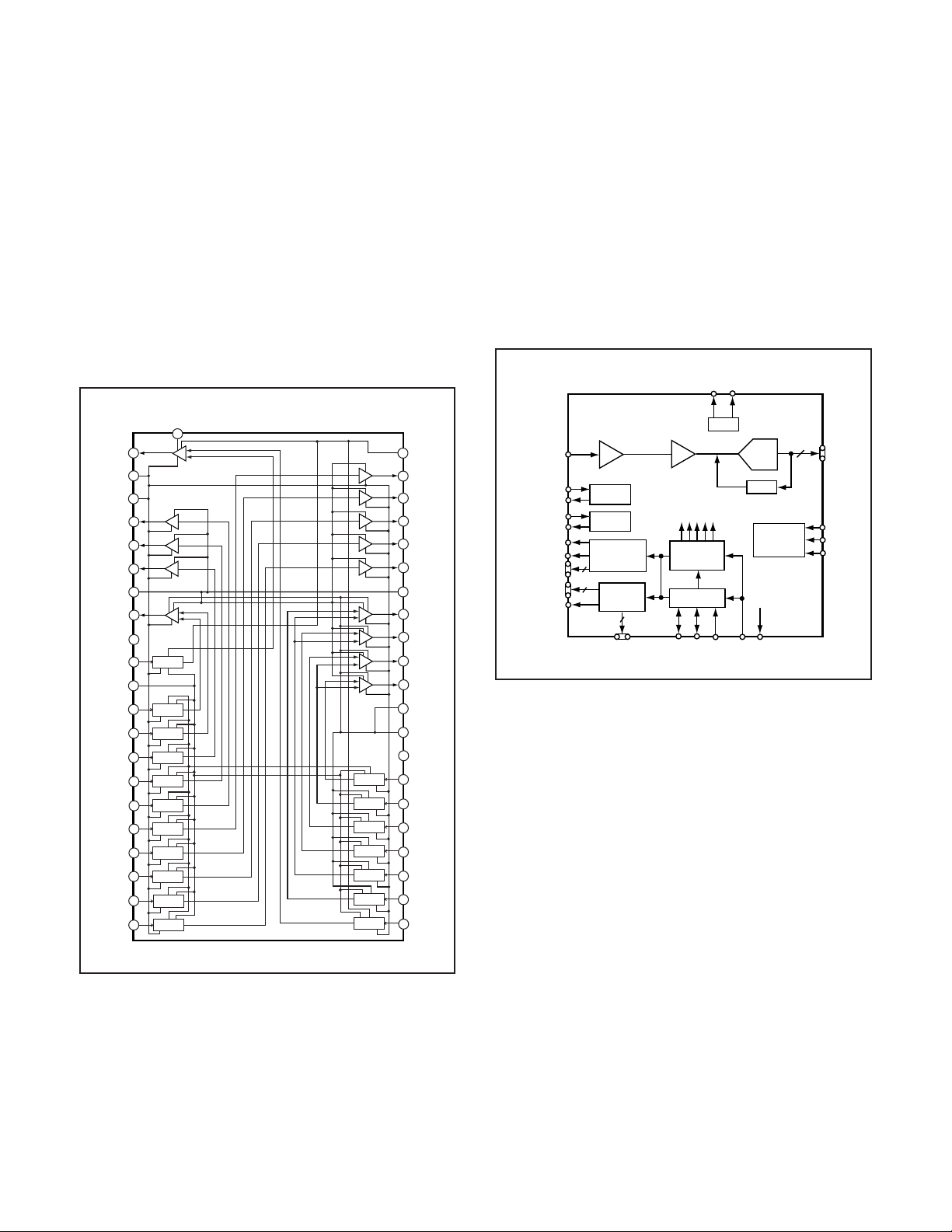
Pin No.
Symbol Pin Description
Fig. 1-1.Optical Black Location (Top View)
Photo diode
10
VDD
VO
GND
13
14
15
Vertical shift register
Output part
Horizontal shift register
16
RG
ø
20
21
22
H2
H1
HL
ø
ø
ø
11
12
23
24
17
18
19
Fig. 1-2. CCD Block Diagram
Waveform
Voltag e
ø
1
ø
2
ø
3
ø
4
ø
5
ø
6
ø
7
ø
8
9
ø
ø
ø
GND
ø
ø
PT
SUBSW
ø
V6
V5B
V5A
V4
V3B
V3A
V3L
V3R
V2
V1
V1S
V5R
V5L
Vsub
1, 23, 24
2, 3
4, 7, 8, 9, 11
5, 6, 10
14
13
16
12, 15
17
18
19
20, 21
22
5L, V5R, V6
V
5A, V5B Vertical register transfer clock
V
V1S, V2, V3L,
V3R, V4
V
1, V3A, V3B
VO
VDD
ØRG
GND
PT
Vertical register transfer clock
Vertical register transfer clock
Vertical register transfer clock
Signal output
Circuit power DC 12 V
Reset gate clock
GND
Protection transister bias
Substrate controlSUB SW
SUB
L, H1
H
H
Substrate clock
Horizontal register transfer clock
Horizontal register transfer clock
2
Table 1-1. CCD Pin Description
-6.0 V, 0 V
-6.0 V, 0 V, 12 V
-6.0 V, 0 V
-6.0 V, 0 V, 12 V
DC
Aprox. 12 V
4.5 V, 7.8 V
GND 0 V
DC
-6.0 V
0, 3.3 V (When importing all
picture element: 3.3 V)
DC
Aprox. 6 V
(Different from every CCD)
0 V, 3.3 V
0 V, 3.3 V
When sensor read-out
– 2 –
Page 2
3. Part of IC905 (generation of vertical transfer clock,
H Driver) and IC901 (V Driver)
An H driver (part of IC905) and V driver (IC901) are necessary in order to generate the clocks (vertical transfer clock,
horizontal transfer clock and electronic shutter clock) which
driver the CCD.
IC905 has the generation of horizontal transfer clock and the
function of H driver, and is an inverter IC which drives the
horizontal CCDs (H1 and H2). It carries out generating vertical transfer clock, and output to IC901.
In addition the XV1-XV6 signals which are output from IC905
are vertical transfer clocks, and the XSG signal is superimposed onto XV1, XV3 and XV5 at IC901 in order to generate
a ternary pulse. In addition, the XSUB signal which is output
from IC101 is used as the sweep pulse for the electronic shutter, and the RG signal which is output from IC905 is the reset
gate clock.
4. IC905 (H Driver, CDS, AGC and A/D converter)
IC905 contains the functions of H driver, CDS, AGC and A/D
converter. As horizontal clock driver for CCD image sensor,
HØ1 (A and B) and HØ2 (A and B) are generated inside, and
output to CCD.
The video signal which is output from the CCD is input to pin
(A6) of IC905. There are sampling hold blocks generated from
the SHP and SHD pulses, and it is here that CDS (correlated
double sampling) is carried out.
After passing through the CDS circuit, the signal passes
through the AGC amplifier (VGA: Variable Gain Amplifier). It
is A/D converted internally into a 14-bit signal, and is then
input to ASIC (IC101). The gain of the VGA amplifier is controlled by pin (A2), (B3) and (C4) serial signal which is output
from ASIC (IC101).
REFB
REFT
OSUB
VM
OV1
RESET
SUBCNT
VDC
CH1
V5R
V5L
V3R
V3L
V1S
CLI
AD9996
14-BIT
ADC
CLAMP
INTERNAL
REGISTERS
CLO
14
DOUT
SL
SCK
SDI
VMSUB
9
3-level
10
VL
5
VL
27
2-level
24OV2
2-level
23OV4
2-level
21OV6
8
3-level
20
28
Level
1
conversion
3
Level
32
conversion
Level
V1
33
conversion
Level
31
V6
conversion
Level
V4
30
conversion
Level
29
V2
conversion
Level
37
conversion
Level
38
conversion
Level
35
conversion
Level
36
conversion
Level
34
conversion
2-level
2-level
2-level
2-level
2-level
3-level
3-level
3-level
3-level
Level
conversion
Level
conversion
Level
conversion
Level
conversion
Level
conversion
Level
conversion
Level
conversion
7
VHH
16
OV5R
15
OV5L
18
OV3R
17
OV3L
19
OV1S
25
VM
12
OV5A
11
OV5B
14
OV3A
13
OV3B
6
VH
26
VH
4
GND
41
CH2
40
V3
39
CH4
44
CH3
43
V5
42
CH5
2
SUB
CCDIN
3V INPUT
1.8V OUTPUT
1.8V INPUT
3V OUTPUT
H1 TO H8
XV1 TO XV24
XSUBCK
RG
HL
CDS
-3dB, 0dB, +3dB
LDO
REG
CHARGE
PUMP
HORIZONTAL
DRIVERS
8
24
VERTICAL
TIMING
CONTROL
8
GP01 TO GP08
Fig. 1-4. IC905 Block Diagram
6~42 dB
VGA
INTERNAL
CLOCKS
PRECISION
TIMING
GENERATOR
SYNC
GENERATOR
VD
HD
VREF
SYNC
Fig. 1-3. IC901 Block Diagram
– 3 –
Page 3

1-2. CP1 CIRCUIT DESCRIPTION
1. Circuit Description
1-1. Digital clamp
The optical black section of the CCD extracts averaged values from the subsequent data to make the black level of the
CCD output data uniform for each line. The optical black section of the CCD averaged value for each line is taken as the
sum of the value for the previous line multiplied by the coefficient k and the value for the current line multiplied by the
coefficient 1-k.
1-2. Signal processor
1. γ correction circuit
This circuit performs (gamma) correction in order to maintain
a linear relationship between the light input to the camera
and the light output from the picture screen.
2. Color generation circuit
This circuit converts the CCD data into RGB signals.
3. Matrix circuit
This circuit generates the Y signals, R-Y signals and B-Y signals from the RGB signals.
4. Horizontal and vertical aperture circuit
This circuit is used gemerate the aperture signal.
1-3. AE/AWB and AF computing circuit
The AE/AWB carries out computation based on a 64-segment
screen, and the AF carries out computations based on a 6segment screen.
1-4. SDRAM controller
This circuit outputs address, RAS, CAS and AS data for controlling the SDRAM. It also refreshes the SDRAM.
1-5. Communication control
1. SIO
This is the interface for the 8-bit microprocessor.
2. PIO/PWM/SIO for LCD
8-bit parallel input and output makes it possible to switch between individual input/output and PWM input/output.
When the TG/SG drives the CCD, picture data passes through
the A/D and CDS, and is then input to the ASIC as 12-bit
data. The AF, AE, AWB, shutter, and AGC value are computed from this data, and three exposures are made to obtain
the optimum picture. The data which has already been stored
in the SDRAM is read by the CPU and color generation is
carried out. Each pixel is interpolated from the surrounding
data as being either Ye, Cy, Mg or B primary color data to
produce R, G and B data. At this time, correction of the lens
distortion which is a characteristic of wide-angle lenses is
carried out. After AWB and γ processing are carried out, a
matrix is generated and aperture correction is carried out for
the Y signal, and the data is then compressed by JPEG and
is then written to card memory (SD card).
When the data is to be output to an external device, it is taken
data from the memory and output via the USB I/F. When played
back on the LCD and monitor, data is transferred from memery
to the SDRAM, and the image is then elongated so that it is
displayed over the SDRAM display area.
3. LCD Block
The LCD display circuit is located on the CP1 board, and
consists of driver (IC171). The video signals (YCrCb) from
the ASIC are input as 8-bit digital signals together with the
synchronization control signals (LCDCLK, LCDVD and
LCDHD). They are converted to RGB inside the driver and
output to the LCD panel. Furthermore, the driver has a builtin DC/DC converter to generate the power supplies (8.5 V
and 5.5 V) that are necessary for the LCD.
4. Lens drive block
4-1. Iris drive
When the drive signals (IIN1 and IIN2) which are output from
the ASIC (IC101), iris motor is driven by the driver (IC956),
and are then used to drive the iris steps.
4-2. Focus drive
When the drive signals (FIN1, FIN2, FIN3 and FIN4) which are
output from the ASIC (IC101), the focus stepping motor is driven
by the driver (IC956). Detection of the standard focusing positions is carried out by means of the photointerruptor (FOCUS
PI) inside the lens block.
1-6. TG/SG
Timing generated for 6 million pixel horizontal addtion CCD
control.
1-7. Digital encorder
It generates chroma signal from color difference signal.
2. Outline of Operation
When the shutter opens, the reset signals (ASIC and CPU)
and the serial signals (“take a picture” commands) from the
8-bit microprocessor are input and operation starts.
4-3. Zoom drive
When the drive signals (ZIN1, ZIN2, ZIN3 and ZIN4) which are
output from the ASIC (IC101), the zoom stepping motor is driven
by the driver (IC956). Detection of the standard zoom positions is carried out by means of photointerruptor (ZOOM PI)
inside the lens block.
4-4. Shutter drive
When the drive signals (SIN1 and SIN2) which are output from
the ASIC (IC101), it is driven regular current by the driver
(IC956).
– 4 –
Page 4

1-3. PWA POWER CIRCUIT DESCRIPTION
1. Outline
This is the main power circuit, and is comprised of the following blocks.
Switching controller (IC501)
Analog system power output (L5001, Q5001)
4.5 V power output (L5005, Q5008)
Digital 3.25 V power output (L5006)
Digital 1.2 V power output (L5007)
Backlight power output (L5008, Q5009)
Motor system power output (IC531, L5301, Q5301)
2. Switching Controller (IC501)
This is the basic circuit which is necessary for controlling the
power supply for a PWM-type switching regulator, and is provided with seven built-in channels, only CH1 (digital system
1.2 V), CH2 (digital 3.25 V), CH4 (4.5 V system), CH5 (ana-
log system) and CH6 (backlight system) are used. Feedback
from digital system 1.2 V (D) (CH1), 3.25 V (D) (CH2), 4.5 V
system (CH4), analog system (CH5) and backlight system
(CH6) power supply outputs are received, and the PWM duty
is varied so that each one is maintained at the correct voltage
setting level.
Feedback for the backlight power (CH6) is provided to the
both ends voltage of registance so that regular current can
be controlled to be current that was setting.
2-1. Short-circuit protection circuit
If output is short-circuited for the length of time determined
by internal fixing of IC501 , all output is turned off. The control
signal (P ON) are recontrolled to restore output.
3. Analog System Power Output
+12 V (A), +3.45 V (A) and -6.0 V (A) are output. Feedback for
the +12 V (A) is provided to the switching controller (Pin (4) of
IC501) so that PWM control can be carried out.
4. Digital 3.25 V Power Output
VDD3 is output. Feedback for the VDD3 is provided to the
swiching controller (Pin (54) of IC501) so that PWM control
can be carried out.
5. Digital 1.2 V Power Output
VDD1.2 is output. Feedback for the VDD1.2 is provided to the
switching controller (Pin (52) of IC501) so that PWM control
to be carried out.
6. 4.5 V System Power Output
4.5 V is output. Feedback for the 4.5 V output is provided to
the switching controller (Pin (2) of IC501) so that PWM control to be carried out.
7. Backlight Power Supply output
Regular current is being transmitted to LED for LCD backlight. Feedback for the both ends voltage of registance that is
being positioned to in series LED are provided to the switching controller (Pin (6) of IC501) so that PWM control to be
carried out.
8. Motor System Power Output
4.8 V is output. Feedback for the 4.8 V output is sent to pin (1)
of IC531 for PWM control to be carried out.
9. Camera charging circuit
If the camera’s power is turned off, play mode and USB connection mode (card reader and pictbridge) setting while it is
connected to the AC adaptor, the battery will be recharged. In
the above condition, a CTL signal is sent from the microprocessor and recharging starts.
– 5 –
Page 5

1-4. ST1 STROBE CIRCUIT DESCRIPTION
1. Charging Circuit
When UNREG power is supplied to the charge circuit and the
CHG signal from microprocessor becomes High (3.3 V), the
charging circuit starts operating and the main electorolytic
capacitor is charged with high-voltage direct current.
However, when the CHG signal is Low (0 V), the charging
circuit does not operate.
1-1. Charging switch
The CHG signal becomes High, Q5406 becomes ON and the
charging circuit starts operating.
1-2. Power supply filter
C5406 constitutes the power supply filter. They smooth out
ripples in the current which accompany the switching of the
oscillation transformer.
1-3. Oscillation circuit
This circuit generates an AC voltage (pulse) in order to increase the UNREG power supply voltage when drops in current occur. This circuit generates a drive pulse with a frequency
of approximately 50-100 kHz. Because self-excited light omission is used, the oscillation frequency changes according to
the drive conditions.
2. Light Emission Circuit
When FLCLT signals are input from the ASIC expansion port,
the stroboscope emits light.
2-1. Emission control circuit
When the FLCLT signal is input to Hi at the emission control
circuit, Q5409 switches on and preparation is made to the
light emitting. Moreover, when a FLCLT signal becomes Lo,
the stroboscope stops emitting light.
2-2. Trigger circuit
The Q5409 is turned ON by the FLCLT signal and light emission preparation is preformed. Simultaneously, high voltage
pulses of several kV are emitted from the trigger coil and applied to the light emitter.
2-3. Light emitting element
When the high-voltage pulse form the trigger circuit is applied to the light emitting part, currnet flows to the light emitting element and light is emitted.
Beware of electric shocks.
1-4. Oscillation transformer
The low-voltage alternating current which is generated by the
oscillation control circuit is converted to a high-voltage alternating current by the oscillation transformer.
1-5. Rectifier circuit
The high-voltage alternating current which is generated at
the secondary side of T5401 is rectified to produce a highvoltage direct current and is accumulated at electrolytic capacitor C5412.
1-6. Voltage monitoring circuit
This circuit is used to maintain the voltage accumulated at
C5412 at a constance level.
After the charging voltage is divided and converted to a lower
voltage by R5405 and R5406, it is output as the monitoring
voltage VMONIT. When VMONIT voltage reaches a specified
level, the CHG signal is switched to Low and charging is interrupted.
– 6 –
Page 6

1-5. SYA CIRCUIT DESCRIPTION
1. Configuration and Functions
For the overall configuration of the SYA block, refer to the block diagram. The SYA block centers around a 8-bit microprocessor
(IC301), and controls camera system condition (mode).
The 8-bit microprocessor handles the following functions.
1. Operation key input, 2. Clock control and backup, 3. Power ON/OFF, 4. Storobe charge control.
Pin
1
2
3
4
5
6
7
8
9
10
11
12
13
14
15
16
17
18
19
20
21
22
23
24
25
26
27
28
29
30
31
32
33
34
35
36
37
38
39
40
41
42 COMREQ/ZBOOT I
Signal
SCK
BACKUP_CTL
BAT_CHG ON
DC IN
LCD PWM
TSEN_CLK
BR MOTOR +
BR MOTOR –
VDD2
VSS2
CHG_LED
SELF_LED
TH ON
BR PI ON
AV JACK
HOT LINE
SCAN IN0
CHGERR
USB CONNECT
SCAN IN1
SCAN IN2
SCAN IN3
NOT USED
BR DET SW
ST_CHG ON
MAIN RESET
PRG ENA/DATA1
AVREF ON
TSEN_LED
CARD
PLLEN
SCAN OUT 2
SCAN OUT 1
SCAN OUT 0
VSS3
VDD3
(DBGP2)
(DBGP1/CLK)
(DBGP0/DATA0)
P ON
BAT_CHG_CNT
I/O
O
O
O
I
O
O
O
O
-
-
O
O
O
O
I
I
I
I
I
I
I
I
O-
I
O
O
I
O
O
I
O
O
O
O
-
-
I
O
O
O
O
Serial clock output
Backup battery charging control
Camera charging control
DC JACK detection
LCD backlight brightness adjustment
Touch sensor clock (66 kHz)
Barrier motor control +
Barrier motor control –
VDD
GND
Charge LED (L= lighting)
Self timer LED (L= lighting)
Battery temperature detection power control (L= ON)
Barrier motor PI power ON/OFF
AV JACK detection
Hot line request from ASIC
Keymatrix input
Camera charging error detection
USB power detection terminal (L= detection)
Key matrix input
Key matrix input
Key matrix input
Barrier motor detection switch
Strobo charging control
System reset (MRST)
Flash rewrite select terminal
AD VREF ON/OFF signal (L= ON)
Touch sensor LED (H= lighting)
Card detection
PLL oscillation ON/OFF
Key matrix output
Key matrix output
Key matrix output
GND
VDD
(Terminal for debugger)
(Terminal for debugger)
(Terminal for debugger)
D/D converter (digital system) ON/OFF signal
Charging currrent control
Command request input (combined with BOOT output)
Outline
– 7 –
See next page
Page 7
43
44
45
46
47
48 BAT_TEMP I Battery temperature detection
49
50
51
52
53
54
55
56
57 XIN
58
59
60
61
62 TSEN_SENSE
63
64
NOT USED O
LCD BL
TH TEMP
TIME OUT
NOT USED
BAT_OFF I
SREQ
SCAN IN 4
BR PI E
RESET I
XCIN
XCOUT
VSS1 -
XOUT
VDD1
BATTERY
VMONIT
SO
SI
O
I
I
O
I
I Key matrix input (interruption)
I
I
O
I
O
- VDD
I
I
I
O
I
-
LCD backlight ON/OFF signal
Internal temperature detection
Camera charging completed detection
-
Battery OFF detection signal input
Serial communication request signal
Barrier motor PI input (interruption)
Microprocessor reset input
Clock oscillation terminal for clock (32.768 kHz)
Clock oscillation terminal for clock (32.768 kHz)
GND
Main clock oscillation terminal (4 MHz)
Main clock oscillation terminal (4 MHz)
Battery voltage detection
Main condenser charging voltage detection
Touch sensor detection
Serial data output
Serial data input
Table 5-1. 8-bit Microprocessor Port Specification
2. Internal Communication Bus
The SYA block carries out overall control of camera operation by detecting the input from the keyboard and the condition of the
camera circuits. The 8-bit microprocessor reads the signals from each sensor element as input data and outputs this data to the
camera circuits (ASIC) as operation mode setting data. Fig. 5-1 shows the internal communication between the 8-bit microprocessor, ASIC and SPARC lite circuits.
MAIN RESET
S. REQ
8-bit
Microprocessor
ASIC SO
ASIC SI
ASIC SCK
PLLEN
ASIC
Fig. 5-1 Internal Bus Communication System
– 8 –
Page 8

3. Key Operaiton
For details of the key operation, refer to the instruction manual.
SCAN
SCAN
OUT
IN
0
0
← LEFT
123
↑ UP
→ RIGHT
↓ DOWN
4
OK
1
2
MENU
1st
-
2nd
Table 5-2. Key Operation
TELE
PW_TEST
WIDE
TEST
PLAY
PW-ON
4. Power Supply Control
The 8-bit microprocessor controls the power supply for the overall system.
The following is a description of how the power supply is turned on and off. When the battery is attached, a regulated 3.2 V
voltage is normally input to the 8-bit microprocessor (IC301) by IC302, so that clock counting and key scanning is carried out
even when the power switch is turned off, so that the camera can start up again. When the battery is removed, the 8-bit microprocessor operates in sleep mode using the backup lithium secondary battery. At this time, the 8-bit microprocessor only carries
out clock counting, and waits in standby for the battery to be attached again. When a switch is operated, the 8-bit microprocessor
supplies power to the system as required.
The 8-bit microprocessor first sets the P ON signal at pin (40) to high, and then turns on the DC/DC converter. After this, high
signals are output from pins (26) and (31) so that the ASIC is set to the active condition. Once it is completed, the ASIC returns
to the reset condition, all DC/DC converters are turned off and the power supply to the whole system is halted.
LCD
MONITOR
+15 V (L)
Power voltage
Power OFF
ASIC,
memory
3.3 V
OFF
CCD
5 V (A)
+15 V (A) etc.
OFF
8 bit
CPU
3.2 V
(ALWAYS)
32KHz OFF
Power switch ON-
Auto power OFF
CAMERA
Note) 4 MHz = Main clock operation, 32 kHz = Sub clock operation
Shutter switch ON
LCD finder
Play back
Table 5-3. Camera Mode (Battery Operation)
OFF
ON
ON
ON
ON
ON
ON
OFF
4 MHz ON
4 MHz ON
4 MHz ON
4 MHz ON
5. 16-bit A/D circuit (Audio)
This circuit converts the audio signals (analog signals) from the microphone to 16-bit digital signals.
6. 16-bit D/A circuit (Audio)
The audio signals which were converted to digial form by the 16-bit A/D circuit are temporarily to a sound buffer and then
recorded in the SSFDC card. During playback, the 16-bit D/A circuit converts these signals into analog audio signals.
– 9 –
Page 9
2. DISASSEMBLY
2-1. REMOVAL OF CABINET FRONT AND CP1 BOARD
1. Three screws 1.7 x 5
2. Three screws 1.7 x 4
3. Cabinet front
4. Holder cover baria
5. Cover lens
6. FPC
7. Two screws 1.7 x 5
8. Assy motor barrier
9. Remove the solder. (speaker)
13
3
11
10. Remove the solder. (microphone)
11. Remove the solder.
12. Three FPCs
13. Screw 1.7 x 2.5
14. Screw 1.7 x 3.5
15. Connector
16. CP1 board
17. Holder motor
2
12
B
14
A
15
2
A
NOTE: Discharge a strobe capacitor
with the discharge jig (VJ8-0188) for
electric shock prevention.
B
17
16
10
9
6
8
1
a
5
b
7
4
When assembling,
tighten the screws order.
a → b
– 10 –
Page 10

2-2. REMOVAL OF LENS ASSEMBLY
1. Dec right
2. Microphone
3. Two screws 1.7 x 3.5
4. Flexible PWB CP1 & TB1
5. Shaft strap
6. Cover battery
7. Dec bottom
8. Dec left
9. Two screws 1.7 x 2.5
10. Lens assy
4
9
8
10
When assembling,
assemble order.
a → b
1
3
b
5
2
a
7
6
– 11 –
Page 11

2-3. REMOVAL OF LCD, TB1 BOARD AND CABINET BACK
1. Three screws 1.7 x 3.5
2. Spacer VF2
3. FPC
4. Remove the solder.
5. LCD
6. Button set
7. TB1 board
8. Dec card access
9. Button menu
10. Dec button set
11. Button zoom
12. Cabinet back
11
8
12
1
7
b
c
a
2
When assembling,
tighten the screws order.
a → b → c
4
6
9
3
10
5
– 12 –
Page 12

2-4. REMOVAL OF TB2 BOARD AND ST1 BOARD
10
9
11
12
1. Screw 1.7 x 3.5
2. TB2 board
3. Screw 1.7 x 3
4. Dec top
5. ST1 board
4
6
14
6. Spacer ST power
7. Button power
8. Dec button power
9. Spring shutter
10. Button shutter
8
22
11. Holder button shutter
12. Dec top LED
13. Remove the solder.
14. Screw 1.7 x 2.5
15. Remove the solder.
16. Assy lamp
17. Holder flash
18. Three screws 1.7 x 3
19. Stand
20. Two screws 1.7 x 3.5
21. Holder monitor
22. Two screws 1.7 x 2.5
23. Holder strap
24. Speaker, 8
25. Holder battery
a
7
5
b
21
20
13
15
23
17
24
3
16
25
19
1
2
When assembling,
tighten the screws order.
a → b
18
– 13 –
Page 13

2-5. BOARD LOCATION
TB1 board
ST1 board
TB2 board
CP1 board
– 14 –
Page 14

3. ELECTRICAL ADJUSTMENT
Firmware
Data
AWB
Focus
UV Matrix
RGB Odd
RGB Gain
Tint
RGB Even
VCOMDC
Phase
LCD
Calibration
Upload
PAF Cal.
LCD Type
H AFC Test
VCOMPP(LOW)
VCOMPP(HI)
Cal Data
Cal Mode
OK
OK
EVF
USB storage
Get
Set
VID
Set
PID
Set
Serial
Set
Rev.
Set
Setting
Language
Video Mode
VCO
Factory Code
Backrush pulse :
Set
Get
3-1. Table for Servicing Tools
Ref. No.
J-1
J-2
J-3
J-4
J-5
J-6
Name
Pattern box (color viewer)
Calibration software
Chroma meter
Spare lump
Discharge jig
Collimator
Number
1
1
1
1
1
1
Part code
VJ8-0190
VJ8-0263
VJ8-0192
VJ8-0191
VJ8-0188
VJ8-0260
3-4. Setup
1. System requirements
Windows 98 or Me or 2000 or XP
IBM R -compatible PC with pentium processor
CD-ROM drive
3.5-inch high-density diskette drive
USB port
40 MB RAM
Hard disk drive with at least 15 MB available
VGA or SVGA monitor with at least 256-color display
Note: J-1 Pattern box (color viewer) is 100 - 110 VAC only.
J-1 J-2
J-3
J-4
J-5
2. Installing calibration software
1. Insert the calibration software installation diskette into your
diskette drive.
2. Open the explorer.
3. Copy the DscCalDI_150 folder on the floppy disk in the FD
drive to a folder on the hard disk.
3. Installing USB driver
Install the USB driver with camera or connection kit for PC.
4. Pattern box (color viewer)
Turn on the switch and wait for 30 minutes for aging to take
place before using Color Pure. It is used after adjusting the
chroma meter (VJ8-0192) adjust color temperature to 3100 ±
20 K and luminosity to 900 ± 20 cd/m
2
. Be careful of handling
the lump and its circumference are high temperature during
use and after power off for a while.
5. Computer screen during adjustment
3-2. Equipment
1. Oscilloscope
2. Digital voltmeter
3. AC adaptor
4. PC (IBM R -compatible PC, Pentium processor, Window
98 or Me or 2000 or XP)
3-3. Adjustment Items and Order
1. IC501 Oscillation Frequency Adjustment
2. Lens Adjustment
3. AWB Adjustment
4. CCD White Point Defect Detect Adjustment
5. CCD Black Point And White Point Defect Detect Adjust-
ment In Lighted
Note: Item 2-5 adjustments should be carried out in sequence.
3-5. Connecting the camera to the computer
1. Line up the arrow on the cable connector with the notch on
the camera's USB port. Insert the connector.
2. Locate a USB port on your computer.
3. Insert the AC adaptor’s cable to DC jack.
4. If “USB CONNECTION” is displayed, choose the “CARD
READER”, and press the SET button.
– 15 –
Page 15

3-6. The adjustment item which in necessary in part exchange
IC501
Oscillation
Frequency
Adjustment
COMPL PWB CP-1
(636 089 9087)
COMPL PWB ST-1
(636 089 9100)
COMPL PWB TB-1
(636 089 9117)
COMPL PWB TB-2
(636 089 9124)
LENS ASSY
(645 080 4755)
3-7. Adjust Specifications
[CP1 board (Side B)]
Lens
Adjustment
AWB
Adjustment
CL501
CCD White
Point Defect
Detect
Adjustment
CCD Black
Point And White
Point Defect
Detect
Adjustment In
Lighted
Factory
Cord
Setting
2. Lens Adjustment
Language
Setting
USB storage
information
registration
Reset
Setting
VR501
Note:
1. Frequency adjustment is necessary to repair in the CP1
board and replace the parts.
Preparation:
1. Remove the cabinet front. You can see VR501 and CL501
in the CP1 board.
2. Insert the SD card.
3. Turn on the power switch, and set the camera mode.
1. IC501 Oscillation Frequency Adjustment
Measuring Point
Measuring Equipment
ADJ. Location
ADJ. Value
Adjustment method:
1. Adjust with VR501 to 499.5 ± 1 kHz.
CL501
Frequency counter
VR501
499.5 ± 1 kHz
Camera
Collimator
Preparation:
POWER switch: ON
If using a ready-made collimator, set to infinity.
Note:
Do not vibrate during the adjustment.
Adjustment method:
1. Set the camera 0 cm from the collimator. (Do not enter any
light.)
2. Set the camera so that it becomes center of the screen in
the collimator.
3. Double-click on the DscCalDi.exe.
4. Click the Focus, and click the Yes.
5. Lens adjustment value will appear on the screen.
6. Click the OK.
– 16 –
Page 16

DscCalDi
x
Dsc Calibration
x
Focus Result
!
STD_AFPOS=1038
FOCUS=0,-11,9,14
OK
Adjustment value determination is effectuated using the "STD
AFPOS" and "FOCUS" values.
If FOCUS=focus1, focus2, focus3, focus4 and the adjustment
values fulfill the conditions below, they are determined as within
specifications.
Adjustment value determination
997<=STD_AFPOS<=1097
focus1 = 0, -20<=focus2<=+25
-40<=focus3<=+45, -30<=focus4<=+35
3. AWB Adjustment
AWB Result:
1:
AGC=176,345,513,682,852
4F_AGC=0,0,0
WB=278,512,648
CHECK=127,128,142
MS=1728,2102
Adjustment value determination is effectuated using the "AGC",
“CHECK" and "MS" values.
If AGC=a1, a2, a3, a4, a5, CHECK=wc0, wc1, wc2 and
MS=MS1, MS2, the adjustment values fulfill the conditions below, they are determined as within specifications.
Adjustment value determination
50<a1<310, 100<a2<550, 200<a3<750,
300<a4<950, 400<a5<1024
wc0=128 ± 2, wc1=128 ± 2, wc2=130 ± 40
1550<MS1<3850
450<MS2<2750
Adjustment values other than the above are irrelevant.
OK
Copy
Camera
Pattern box
(color viewer)
Preparation:
POWER switch: ON
Adjusting method:
1. When setting the camera in place, set it to an angle so that
nothing appears in any part of the color viewer except the
white section. (Do not enter any light.)
2. Double-click on the DscCalDi.exe.
3. Click the AWB, and click the Yes.
4. AWB adjustment value will appear on the screen.
5. Click the OK.
4. CCD White Point Defect Detect Adjustment
Preparation:
POWER switch: ON
Adjustment method:
1. Double-click on the DscCalDi.exe.
2. Select “CCD Defect” on the LCD “Test”, and click the “Ye s ”.
3. After the adjustment is completed, OK will display.
4. Click the OK.
5. CCD Black Point And White Point Defect Detect
Adjustment In Lighted
Camera
– 17 –
Pattern box
(color viewer)
Page 17

Preparation:
POWER switch: ON
Setting of pattern box:
Color temperature: 3100 ± 20 (K)
Luminance: 900 ± 20 (cd/m
2
)
Adjusting method:
1. Set the camera 0 cm from the pattern box. (Do not enter
any light.)
2. Double-click on the DscCalDi.exe.
3. Select “CCD Black” on the LCD “Test”, and click the “Ye s ”.
4. After the adjustment is completed, the number of defect
will appear.
3-12. Firmware uploading procedure
1. Uploading the firmware should be carried out if the version
number (COMPL PWB XX-X) on the replacement circuit
board is lower than the version of the distributed firmware.
For XX-X, enter the name of the circuit board containing the
firmware.
2. The firmware is distributed by e-mail in self-extracting archive
format. Change the extension of the distributed file to .EXE
and save it in your preferred folder.
3. When you double-click the saved file, the firmware (binary
file) will be saved in the same folder.
4. The firmware must not be distributed without permission.
3-8. Factory Code Setting
1. Check the "Factory Code" display within the Setting group.
2. For U.S.A., Canada and NTSC general area
If "FC_SANYO_U" does not appear, click on the " " mark
located on the right of the "Factory Code" display BOX and
select "FC_SANYO_U".
3. For Europe and PAL general area
If "FC_SANYO_EX" does not appear, click on the " " mark
located on the right of the "Factory Code" display BOX and
select "FC_SANYO_EX".
3-9. Language Setting
1. Click on the " " mark located on the right of the
"Language" display BOX.
2. Select language. (Default is English.)
3. End "DscCal" and remove the camera before turning the
camera power OFF.
Calibration
AWB
Focus
UV Matrix
Cal Mode
Cal Data
USB storage
VID
Get
PID
Set
Backrush pulse :
OK
OK
Upload
Firmware
Data
PAF Cal.
EVF
LCD Type
Get
LCD
RGB Odd
RGB Gain
Tint
VCO
H AFC Test
Serial
Set
Set
Rev.
RGB Even
VCOMDC
Phase
Set
Set
Set
VCOMPP(LOW)
VCOMPP(HI)
Setting
Language
Video Mode
Factory Code
3-10. Reset Setting
Carry out reset settings after replacing CP1 board.
1. Turn on the camera.
2. Press the MENU button.
3. Choose the OPTION.
4. Choose the RESET SETTINGS, and press the SET
button.
5. Select Yes, and press the SET button.
3-11. The Compulsive boot starting method
1. Keep MENU button, SET button, and SHUTTER button depressed while switching on the power.
2. Connect the camera and the computer with USB cable.
1. Overwriting firmware from the SD card
Preparation:
SD card: SD card with firmware rewritten into the root directory
Data: S811Nxxx.BIN (xxx: version)
Overwriting method:
1. Insert the above SD card.
2. Turn on the camera.
3. Press the PLAY button.
4. Press the MENU button. The playback setting screen appears.
5. Choose the OPTION icon.
6. Choose the FORMAT.
7. Toggle the SET button to the left for 2 seconds. FIRMWARE
UPDATE will display.
8. Choose YES.
9. Press the SET button. Update is starting.
Note:
Do not turn off the camera’s power or remove the SD card
while the firmware is being updated.
The power will turn on automatically after the update is complete.
2. Overwriting firmware from the calibration software
Preparation:
PC with overwriting firmware copied to the preferred folder in
the HD.
Data: S811Nxxx.BIN (xxx: version)
Overwriting method:
1. Connect the camera’s USB/AV terminal to the computer’
USB connector.
2. The USB Connection screen appears on the camera’s LCD
monitor. Choose the “CARD READER”, and press the SET
button.
3. Double-click on the DscCalDi.exe.
4. Click the Firmware.
5. Choose the fimware file to use for overwriting, and click
the Yes.
5. Update is starting. The message will appear, and choose
OK.
6. After the update is complete, disconnect the USB cable
and turn the camera’s power off.
Note:
Do not turn off the camera’s power while the firmware is being updated.
– 18 –
Page 18

4. USB STORAGE INFORMATION REGISTRATION
USB storage data is important for when the camera is connected to a computer via a USB connection.
If there are any errors in the USB storage data, or if it has not
been saved, the USB specification conditions will not be satisfied, so always check and save the USB storage data.
Preparation:
POWER switch: ON
Adjustment method:
1. Connect the camera to a computer. (Refer to 3-5. Connecting the camera to the computer on the page 15.)
2. Double-click on the DscCalDi.exe.
3. Click on the Get button in the USB storage window and
check the USB storage data.
VID: SANYO
PID: E6
Serial:
Rev. : 1.00
4. Check the “Serial” in the above USB storage data. If the
displayed value is different from the serial number printed
on the base of the camera, enter the number on the base
of the camera. Then click the Set button.
5. Next, check VID, PID and Rev. entries in the USB storage
data. If any of them are different from the values in 3. above,
make the changes and then click the corresponding Set
button.
Calibration
AWB
Focus
UV Matrix
Cal Mode
Cal Data
USB storage
VID
Get
PID
Set
Backrush pulse :
OK
OK
Upload
Firmware
Data
PAF Cal.
EVF
LCD Type
Get
LCD
RGB Odd
RGB Gain
Tint
VCO
H AFC Test
Serial
Set
Set
Rev.
RGB Even
VCOMDC
Phase
Set
Set
Set
VCOMPP(LOW)
VCOMPP(HI)
Setting
Language
Video Mode
Factory Code
– 19 –
Page 19

5. TROUBLESHOOTING GUIDE
POWER LOSS INOPERTIVE
SET THE MAIN
SWITCH ON
IC301-51
(SCAN IN4)
PULSE INPUT
NO
IC302-7 4.7 V
(BOOST 4.7 V)
YES
IC301-59
(VDD)
HIGH
IC301-53
(RESET)
HIGH
IC301-49
(BAT OFF)
HIGH
IC301-58
OSCILLATION
YES
IC301-55
OSCILLATION
YES
YES
NO
LOW
LOW
LOW
NO
NO
CHECK S3302
CHECK IC531, Q5301
CHECK IC302
CHECK IC302, RB305
CHECK IC302, RB305
CHECK X3001
CHECK X3002
TAKING INOPERATIVE
PUSH SHUTTER
BUTTON
IC301-17, 20
(SCAN IN 0, 1)
PULSE INPUT
YES
IC301-40
(P ON)
HIGH
SERIAL
COMMUNICATION
OK
CHECK CP1 DMA
BLOCK
NO
LOW
NG
CP1 DMA BLOCK
CHECK S3301
CHECK IC301
CHECK IC301,
CHECK IC301
NO PICTURE
CLK (48 MHz)
OSCILLATION
OK
IC301-63, 64
(ASIC_SO, ASIC_SI)
OK
CHECK CP1
NG
NG
CHECK X1102
INCORRECT HANDSHAKING
BETWEEN 8-BIT CPU AND ASIC
CHECK EACH INTERFACE
– 20 –
Page 20

6. PARTS LIST
ACCESSOEIES
LOCATION P ARTS NO. DESCRIPTION LOCA TION PARTS NO. DESCRIPTION
1 636 076 5344 STRAP-SX713/J
2 645 079 1352 CABLE,DSC A/V,EXCEPT VPC-E6,VPC-E6U
2 645 081 6185 CABLE,DSC A/V-PRINTED,VPC-E6,VPC-E6U
3 645 079 1369 CABLE,DSC USB,EXCEPT VPC-E6,VPC-E6U
3 645 078 0943 CABLE,DSC USB-PRINTED,VPC-E6,VPC-E6U
4 645 057 1503 CORD,POWER-1.2MK,VPC-E6EX,
VPC-E6EXW,VPC-E6GX,VPC-E6GXW
4 645 076 0228 CORD,POWER-1.5MK,VPC-E6,VPC-E6U
4 645 076 0235 CORD,POWER-1.5MK,VPC-E6EX,
VPC-E6EXW,VPC-E6GX,VPC-E6GXW
5 645 080 1846 ADAPTOR,AC-DC
6 645 063 5816 BATTERY,RECHARGE, LI-ION
7 645 080 4397 DISC,CD-ROM SSP 811 U
(APPRICATION SOFTWARE) (PDF INSTRUCTION
MANUAL: English, French, Spanish, German, Dutch,
Italy, Chinese Traditional, Chinese Simplified, Korean,
Russian)
9053 636 090 4606 INSTRUCTION MANUAL (English)
(CAMERA, APPRICATION SOFTWARE)
123
P ACKING MATERIALS
7001 636 093 0087 CARTON INNER-SX811/EX,
VPC-E6EX,VPC-E6EXW,VPC-E6GX,VPC-E6GXW
7001 636 090 6433 CARTON INNER-SX811/U,VPC-E6 ONLY
7001 636 093 2876 CARTON INNER-SX811/U3,VPC-E6U ONLY
7002 636 078 4659 CUSHION SHEET-SX792/KRNK
7003 636 090 6426 REINFOECE PAD,A-SX811/J
4
5
6
7
21
Page 21

CABINET AND CHASSIS PARTS 1
LOCA TION PARTS NO. DESCRIPTION LOCA TION PARTS NO. DESCRIPTION
1 636 089 6611 DEC FRONT RING-SX811/J
2 636 089 8257 ADHESIVE DEC FRONT-811/J
3 636 089 6574 CABINET FRONT-SX811/J,
VPC-E6EXW,VPC-E6GXW
3 636 092 0545 CABINET FRONT-SX811/J,
VPC-E6,VPC-E6EX,VPC-E6GX
3 636 092 4550 CABINET FRONT-SX811/U, VPC-E6U ONLY
4 636 090 2497 ADHESIVE DEC FLASH-811/J
5 636 090 3753 SPACER DEC FLASH-SX811/J
6 636 089 6635 DEC FLASH-SX811/J
7 636 089 6628 DEC SELF LED-SX811/J
8 636 090 6419 SPACER FRONT PWB B-SX811
9 636 093 0681 SPACER FRONT STRAP-SX811
10 636 089 8417 SPACER DC FRONT-SX811/J
11 636 092 5267 ADHESIVE FRONT INNER-811
12 636 089 6772 HOLDER FRONT INNER-811/J
13 636 090 5986 SPACER COVER LENS-SX811/J
14 636 089 6857 HOLDER MOTOR -SX811/J
15 636 089 8288 ADHESIVE HOLDER MOTOR-811
16 636 089 9087 COMPL PWB,CP-1
17 636 092 2938 HOLDER COVER BATT -SX811/J
18 636 092 3225 ADHESIVE COVER BATT -811/J
19 636 089 6604 COVER BATTERY-SX811/J
20 636 089 6710 DEC BOTTOM-SX811/J
21 636 071 6421 SHAFT STRAP-SX786/JNK
22 645 080 4144 MICROPHONE
23 636 089 6703 DEC RIGHT-SX811/J
24 636 089 6697 DEC LEFT-SX811/J
25 636 089 6833 HOLDER COVER BARIA-SX811/
26 636 089 6598 COVER LENS-SX811/J
27 645 079 2410 ASSY,MOTOR BARRIER-SX811/
28 645 079 2397 LCD(L4S00222P00)
29 636 090 3784 SPACER BACK LIGHT2-SX811/
30 636 092 3911 SP ACER BACK LIGHT-SX811/J
31 636 089 9513 ASSY,WIRE JW172&LCD-SX811
32 636 089 9520 ASSY,WIRE JW171&LCD-SX811
33 636 092 7339 SPACER MONITOR SIDE-SX811
34 636 090 3425 FLEXIBLE PWB CP-1&TB-1
35 636 083 4163 SPACER VF2-SX718/J
36 636 089 9117 COMPL PWB,TB-1
37 636 089 6529 BUTTON SET-SX811/J
38 636 089 8431 SPACER MONITOR-SX811/J
39 636 089 6642 DEC BUTTON SET-SX811/J
40 636 089 6505 BUTTON MENU-SX811/J
41 636 089 6659 DEC CARD ACCESS-SX811/J
42 636 089 6581 CABINET BACK-SX811/J
43 636 089 6512 BUTTON ZOOM-SX811/J
44 636 089 6741 DEC MONITOR-SX811/J
101 411 177 0906 SCR S-TPG PAN PCS 1.7X3.5
102 411 176 1003 SCR PAN PCS 1.7X2.5
103 411 204 2705 SCR TIN 1.7X5
104 411 204 2606 SCR TIN 1.7X4
105 411 176 6909 SCR S-TPG PAN PCS 1.7X5.0
22
Page 22

Cabinet 1
4
1
43
42
44
41
40
33
39
37
01
29
36
32
104
38
101
35
31
30
24
28
23
101
102
16
34
29
10
101
15
20
105
27
21
101
22
19
6
514
9
4
103
25
26
105
10
18
17
13
4
12
3
11
8
7
1
2
SX811/J
Ver.1
2005.08
23
Page 23

CABINET AND CHASSIS PARTS 2
LOCA TION PARTS NO. DESCRIPTION
1 636 090 7898 COMPL,CA1 SV-SX811
2 636 089 9124 COMPL PWB,TB-2
3 636 089 6901 SPRING LOCK LEVER-SX811/J
4 636 075 7998 LEVER LOCK BATTERY-SX713J
5 636 089 6925 SPRING COVER BATT SX811/J
6 636 089 6932 SPRING BATT EJECT-SX811/J
7 636 089 6871 STAND-SX811/J
8 636 089 6826 HOLDER BATTERY-SX811/J
9 636 090 5955 LABEL COUTION BATT-SX811
10 636 089 8271 ADHESIVE SPEAKER-SX811/J
11 645 079 5718 SPEAKER,8
12 636 089 6789 HOLDER MONITOR-SX811/J
13 636 089 6765 HOLDER STRAP-SX811/J
14 645 081 7663 ASSY,LAMP-SX811
15 636 089 6819 HOLDER FLASH-SX811/J
16 636 089 9100 COMPL PWB,ST-1
17 636 090 3821 SPACER MAINCON A-SX811
18 636 090 5962 SPACER MAINCON B-SX811
19 636 092 7285 SPACER ST1-SX811
20 636 090 7317 SPACER SHUTTER-SX811/J
21 636 089 6796 HLD PLATE SHUTTER-SX811/J
22 636 064 4977 SPRING SHUTTER-SX541/JM
23 636 089 6536 BUTTON SHUTTER-SX811/J
24 636 089 6802 HOLDER BUTTON SHUTTER-811
25 636 089 6680 DEC TOP LED-SX811/J
26 636 093 3507 SPACER ST POWER-SX811/J
27 636 089 6673 DEC BUTTON POWER-811/J
28 636 089 6543 BUTTON POWER-SX811/J
29 636 093 3453 SPACER TOP BACK-SX811
30 636 089 6666 DEC TOP-SX811/J, EXCEPT VPC-E6U
30 636 092 4581 DEC TOP-SX811/U, VPC-E6U ONLY
101 411 177 0906 SCR S-TPG PAN PCS 1.7X3.5
102 411 176 1003 SCR PAN PCS 1.7X2.5
106 411 177 9503 SCR S-TPG PAN PCS 1.7X3
107 411 189 5609 SCR S-TPG TIN PCS 1.7X2.5
108 411 176 6701 SCR S-TPG PAN PCS 1.7X2.5
24
Page 24

Cabinet 2
2
30
24
16
18
22
21
20
17
23
25
19
26
107
108
14
107
27
28
13
11
15
10
29
102
102
101
1
106
101
2
9
8
7
5
106
1
6
3
4
106
SX811/J
Ver.1
2005.08
25
Page 25

ELECTRICAL PARTS
Note:
1. Materials of Capacitors and Resistors are abbreviated as follows ;
Resistors Capacitors
MT-FILM Metallized Film Resistor MT-POLYEST Metallized Polyester Capacitor
MT-GLAZE Metallized Glaze Resistor MT-COMPO Metallized Composite Capacitor
OXIDE-MT Oxide Metallized Film Resistor TA-SOLID Tantalum Solid Capacitor
2. Tolerance of Capacitor (10pF over) and Resistor are noted with follow symboles.
F ............1% G ............2% J ............5% K ............10%
M ..........20% N ..........30% Z ..........+80% ~ -20%
3. Capacitors
U : µF P : pF
4. Inductors
UH : µH MH : mH
5. N.S.P. : Not available as service parts.
LOCA TION PARTS NO. DESCRIPTION LOCA TION PARTS NO. DESCRIPTION
COMPL PWB,CP-1
636 089 9087
(RECHARGEABLE BATTERY)
Z3001 645 051 6009 BATTERY,RECHARGE
(VARISTORS)
VA134 408 050 0504 VARISTOR AVR-M1005C080MT
VA135 408 050 0504 VARISTOR AVR-M1005C080MT
VA136 408 053 2208 VARISTOR AVRL101A6R8GT
VA137 408 053 2208 VARISTOR AVRL101A6R8GT
VA303 408 050 0504 VARISTOR AVR-M1005C080MT
(SEMICONDUCTORS)
Q1303 405 172 4700 TR UNR32A3
OR 405 168 3700 TR DTC144EM
OR 405 207 5009 TR RN1104FV
Q1403 405 167 0403 TR EMD12
Q1501 405 168 4509 TR 2SA2029-R
OR 405 168 4608 TR 2SA2029-S
Q1701 405 157 1403 TR 2SA2018
Q3001 405 200 9004 TR EML17
Q3002 405 208 3905 TR EMB11
Q3003 405 172 4700 TR UNR32A3
OR 405 168 3700 TR DTC144EM
OR 405 207 5009 TR RN1104FV
Q3004 405 195 5302 TR DTC123EM
Q3005 405 169 4508 TR DTC114EM
OR 405 207 4903 TR RN1102FV
OR 405 172 4601 TR UNR32A1
Q3006 405 195 5302 TR DTC123EM
Q5001 405 184 6907 TR QS5U17
Q5002 405 200 6003 TR UP03397
Q5003 405 168 3908 TR EMZ1
Q5007 405 169 4508 TR DTC114EM
Q5008 405 183 6700 TR CPH3409-TL-E
Q5009 405 207 4408 TR US5U2
Q5204 405 212 7500 TR RTL030P02
Q5205 405 184 6006 TR UP03396
Q5206 405 206 7707 TR SI3473DV-E3
Q5301 405 210 5508 TR RTL035N03
Q9501 405 182 8507 TR EMH16
Q9509 405 183 7707 TR EMH10
(INTEGRATED CIRCUITS)
IC101 410 585 8306 IC KS755U2464CBP
IC103 409 588 5405 IC EDS2532AABH-75
IC121 409 643 8808 IC K5V3228VTM-D976
IC151 409 638 7601 IC BH76806FVM
IC171 409 651 9804 IC LC15016A-EV
IC181 409 609 8606 IC BH6412KN-E2
IC182 409 505 9400 IC TK11130CS
IC301 410 595 4008 IC LC875924A-57D5-E
IC301 410 587 2609 IC LC87F5932A-F57D5-E
AL-SOLID Aluminum Solid Capacitor
NP-ELECT Non-Polarized Electrolytic Capacitor
OS-SOLID Aluminum Solid Capacitors with Organic
Semiconductive Electrolytic Capacitor
DL-ELECT Double Layered Electrolytic Capacitor
IC302 409 582 6200 IC BD4289FVM
IC501 409 651 7503 IC FA7724R-H4
IC502 409 523 0502 IC TK11134CSCL
IC524 409 629 4008 IC LTC4053EDD-4.2PBF
IC531 409 526 4002 IC XC9104D095M
IC901 409 645 9902 IC AN20112A
IC904 409 505 9400 IC TK11130CS
IC905 409 641 4604 IC AD9996BBCZ BGA (N.S.P.)
IC956 409 585 2506 IC BD6757KN-E2
D3002 407 210 1900 DIODE 1SS400
OR 407 226 4803 DIODE BAS516
D3005 407 241 4000 LED SML-511UW,
D5001 407 221 7403 DIODE DAN217U
D5002 407 208 0304 DIODE MA2S111
D5003 407 232 3609 DIODE SD833-04SC
D5005 407 238 1203 DIODE CUS01,Q
D5006 407 238 1203 DIODE CUS01,Q
D5007 407 210 5403 DIODE RB551V-30
D5008 407 246 3602 DIODE RB055LA-40
D5209 407 210 1108 ZENER DIODE UDZS7.5B
D5301 407 246 2803 DIODE SS2P3L-E3
D9001 407 223 5506 DIODE MA2Z720
D9002 407 149 0807 DIODE 1SS355
D9003 407 223 5506 DIODE MA2Z720
D9004 407 223 5506 DIODE MA2Z720
X1102 645 069 4967 OSC,CRYSTAL 48.00000MHZ
X3001 645 046 1415 OSC,CERAMIC 4.00MHZ
X3002 645 054 3791 OSC,CRYSTAL 32.768KHZ
VR501 645 049 3232 VR,SEMI,10K S
L1001 645 020 1912 INDUCTOR,240 OHM
L1002 645 059 8111 IMPEDANCE,1000 OHM P
L1003 645 020 1912 INDUCTOR,240 OHM
L1004 645 020 1912 INDUCTOR,240 OHM
L1080 645 059 8111 IMPEDANCE,1000 OHM P
L1302 645 020 1912 INDUCTOR,240 OHM
L1303 645 020 1912 INDUCTOR,240 OHM
L1304 645 020 1912
L1702 645 037 1523 INDUCTOR,10U K
L5001 645 067 2378 INDUCTOR,10U M
L5002 645 061 7416 INDUCTOR,47U M
L5005 645 059 1068 INDUCTOR,4.7U M
L5006 645 073 6865 INDUCTOR,10U M
L5007 645 067 2354 INDUCTOR,10U M
L5008 645 067 2354 INDUCTOR,10U M
L5301 645 058 0918 INDUCTOR,10U M
L9001 645 059 8111 IMPEDANCE,1000 OHM P
(DIODES)
(OSCILLATORS)
(VARIABLE RESISTOR)
(INDUCTORS)
INDUCTOR,240 OHM
26
Page 26

LOCATION P ARTS NO. DESCRIPTION LOCA TION PARTS NO. DESCRIPTION
CB181 403 392 5507 CERAMIC 1U K 6.3V
(CAPACITORS)
CB901 403 392 5507 CERAMIC 1U K 6.3V
CB902 403 391 4303 CERAMIC 0.1U K 16V
CB903 403 391 4303 CERAMIC 0.1U K 16V
CB951 403 391 4303 CERAMIC 0.1U K 16V
C1002 403 381 8106 CERAMIC 1U K 6.3V
C1003 403 381 8106 CERAMIC 1U K 6.3V
C1010 403 338 0306 CERAMIC 0.1U K 10V
C1012 403 338 0306 CERAMIC 0.1U K 10V
C1013 403 338 0306 CERAMIC 0.1U K 10V
C1014 403 338 0306 CERAMIC 0.1U K 10V
C1015 403 338 0306 CERAMIC 0.1U K 10V
C1017 403 338 0306 CERAMIC 0.1U K 10V
C1018 403 276 1007 CERAMIC 0.01U K 16V
C1019 403 276 1007 CERAMIC 0.01U K 16V
C1020 403 276 1007 CERAMIC 0.01U K 16V
C1021 403 276 1007 CERAMIC 0.01U K 16V
C1028 403 420 7206 CERAMIC 10U K 10V
C1029 403 381 8106 CERAMIC 1U K 6.3V
C1030 403 338 0306 CERAMIC 0.1U K 10V
C1031 403 338 0306 CERAMIC 0.1U K 10V
C1032 403 338 0306 CERAMIC 0.1U K 10V
C1033 403 338 0306 CERAMIC 0.1U K 10V
C1043 403 276 1304 CERAMIC 1000P K 50V
C1082 403 383 5202 CERAMIC 4.7U K 6.3V
C1083 403 381 8106 CERAMIC 1U K 6.3V
C1084 403 381 8106 CERAMIC 1U K 6.3V
C1085 403 381 8106 CERAMIC 1U K 6.3V
C1086 403 381 8106 CERAMIC 1U K 6.3V
C1111 403 314 5301 CERAMIC 5P C 50V
C1112 403 314 5301 CERAMIC 5P C 50V
C1201 403 381 8106 CERAMIC 1U K 6.3V
C1301 403 381 8106 CERAMIC 1U K 6.3V
C1401 403 338 0306 CERAMIC 0.1U K 10V
C1402 403 311 5809 CERAMIC 47P J 50V
C1403 403 311 5809 CERAMIC 47P J 50V
C1404 403 311 5809 CERAMIC 47P J 50V
C1405 403 311 5809 CERAMIC 47P J 50V
C1406 403 311 5809 CERAMIC 47P J 50V
C1501 403 381 8106 CERAMIC 1U K 6.3V
C1502 403 383 5202 CERAMIC 4.7U K 6.3V
C1503 403 381 8106 CERAMIC 1U K 6.3V
C1504 403 381 8106 CERAMIC 1U K 6.3V
C1702 403 393 2604 CERAMIC 22U M 6.3V
C1703 403 420 7503 CERAMIC 4.7U K 16V
C1704 403 408 5507 CERAMIC 2.2U K 16V
C1705 403 382 6309 CERAMIC 1U K 16V
C1706 403 382 6309 CERAMIC 1U K 16V
C1707 403 420 7503 CERAMIC 4.7U K 16V
C1708 403 155 1807 CERAMIC 0.01U K 25V
C1709 403 420 7503 CERAMIC 4.7U K 16V
C1710 403 420 7503 CERAMIC 4.7U K 16V
C1711 403 408 5507 CERAMIC 2.2U K 16V
C1712 403 408 5507 CERAMIC 2.2U K 16V
C1713 403 382 6309 CERAMIC 1U K 16V
C1714 403 276 1007 CERAMIC 0.01U K 16V
C1716 403 338 0306 CERAMIC 0.1U K 10V
C1803 403 383 5202 CERAMIC 4.7U K 6.3V
C1806 403 338 0306 CERAMIC 0.1U K 10V
C1807 403 338 0306 CERAMIC 0.1U K 10V
C1810 403 324 6404 CERAMIC 0.022U K 16V
C1815 403 381 8106 CERAMIC 1U K 6.3V
C1820 403 338 0306 CERAMIC 0.1U K 10V
C1821 403 338 0306 CERAMIC 0.1U K 10V
C1822 403 338 0306 CERAMIC 0.1U K 10V
C1823 403 383 5202 CERAMIC 4.7U K 6.3V
C1824 403 383 5202 CERAMIC 4.7U K 6.3V
C1826 403 383 5202 CERAMIC 4.7U K 6.3V
C1827 403 381 8106 CERAMIC 1U K 6.3V
C1829 403 324 6404 CERAMIC 0.022U K 16V
C1830 403 383 5202 CERAMIC 4.7U K 6.3V
C1831 403 383 5202 CERAMIC 4.7U K 6.3V
C1901 403 383 5202 CERAMIC 4.7U K 6.3V
C1902 403 383 5202 CERAMIC 4.7U K 6.3V
C3001 403 420 7206 CERAMIC 10U K 10V
C3002 403 369 0306 CERAMIC 1U Z 4V
C3003 403 322 1005 CERAMIC 0.1U Z 16V
C3004 403 322 1005 CERAMIC 0.1U Z 16V
C3005 403 338 0306 CERAMIC 0.1U K 10V
C3007 403 381 8106 CERAMIC 1U K 6.3V
C3008 403 276 2806 CERAMIC 18P J 50V
C3009 403 276 1007 CERAMIC 0.01U K 16V
C3010 403 338 0306 CERAMIC 0.1U K 10V
C3011 403 276 1304 CERAMIC 1000P K 50V
C3012 403 317 2307 CERAMIC 20P J 50V
C3013 403 338 0306 CERAMIC 0.1U K 10V
C3014 403 338 0306 CERAMIC 0.1U K 10V
C5001 403 311 3409 CERAMIC 0.01U K 16V
C5003 403 311 7605 CERAMIC 2200P K 50V
C5005 403 381 8106 CERAMIC 1U K 6.3V
C5006 403 381 8106 CERAMIC 1U K 6.3V
C5007 403 381 8106 CERAMIC 1U K 6.3V
C5008 403 311 3409 CERAMIC 0.01U K 16V
C5009 403 381 8106 CERAMIC 1U K 6.3V
C5010 403 381 8106 CERAMIC 1U K 6.3V
C5011 403 346 9803 CERAMIC 0.047U K 10V
C5012 403 314 7404 CERAMIC 3300P K 50V
C5013 403 311 4505 CERAMIC 1000P K 50V
C5014 403 326 2701 CERAMIC 0.015U K 16V
C5041 403 358 3202 CERAMIC 10U K 6.3V
C5042 403 408 5507 CERAMIC 2.2U K 16V
C5044 403 319 3500 CERAMIC 220P K 50V
C5045 403 391 8806 CERAMIC 2.2U K 16V
C5046 403 376 9804 CERAMIC 0.033U K 16V
C5047 403 376 9804 CERAMIC 0.033U K 16V
C5048 403 383 5004 CERAMIC 1U K 16V
C5072 403 381 6201 POS-SOLID 33U M 8V
C5073 403 346 9803 CERAMIC 0.047U K 10V
C5075 403 338 0306 CERAMIC 0.1U K 10V
C5076 403 343 3101 CERAMIC 1U K 6.3V
C5091 403 392 5002 CERAMIC 22U M 6.3V
C5093 403 319 3609 CERAMIC 330P K 50V
C5101 403 392 5002 CERAMIC 22U M 6.3V
C5102 403 344 0406 CERAMIC 0.033U K 10V
C5111 403 383 5004 CERAMIC 1U K 16V
C5112 403 311 4505 CERAMIC 1000P K 50V
C5202 403 372 7507 CERAMIC 2.2U K 6.3V
C5204 403 341 7002 CERAMIC 0.068U K 10V
C5205 403 311 3409 CERAMIC 0.01U K 16V
C5206 403 311 3409 CERAMIC 0.01U K 16V
C5302 403 392 5002 CERAMIC 22U M 6.3V
C5303 403 381 6201 POS-SOLID 33U M 8V
C5304 403 311 7506 CERAMIC 22P J 50V
C9002 403 189 0807 CERAMIC 0.1U K 25V
C9003 403 420 7206 CERAMIC 10U K 10V
C9005 403 391 0800 CERAMIC 1U K 25V
C9006 403 381 8106 CERAMIC 1U K 6.3V
C9010 403 433 4100 TA-SOLID 22U M 10V
C9011 403 338 0306 CERAMIC 0.1U K 10V
C9012 403 338 0306 CERAMIC 0.1U K 10V
C9013 403 338 0306 CERAMIC 0.1U K 10V
C9014 403 338 0306 CERAMIC 0.1U K 10V
C9016 403 338 0306 CERAMIC 0.1U K 10V
C9017 403 433 4100 TA-SOLID 22U M 10V
C9018 403 338 0306 CERAMIC 0.1U K 10V
C9019 403 338 0306 CERAMIC 0.1U K 10V
C9022 403 338 0306 CERAMIC 0.1U K 10V
C9025 403 323 4302 CERAMIC 0.15U K 25V
C9026 403 155 1807 CERAMIC 0.01U K 25V
C9027 403 338 0306 CERAMIC 0.1U K 10V
C9028 403 311 4505 CERAMIC 1000P K 50V
C9029 403 311 4505 CERAMIC 1000P K 50V
C9030 403 311 4505 CERAMIC 1000P K 50V
C9031 403 381 8106 CERAMIC 1U K 6.3V
C9032 403 340 6907 CERAMIC 1U K 16V
C9033 403 343 8700 CERAMIC 1U M 12V
C9034 403 395 0905 CERAMIC 1U M 25V
C9035 403 281 5007 CERAMIC 0.033U K 25V
C9037 403 323 6306 CERAMIC 0.1U K 16V
C9514 403 338 0306 CERAMIC 0.1U K 10V
C9515 403 338 0306 CERAMIC 0.1U K 10V
C9516 403 338 0306 CERAMIC 0.1U K 10V
C9517 403 338 0306 CERAMIC 0.1U K 10V
27
Page 27

LOCA TION PARTS NO. DESCRIPTION LOCA TION PARTS NO. DESCRIPTION
C9518 403 338 0306 CERAMIC 0.1U K 10V
C9519 403 338 0306 CERAMIC 0.1U K 10V
(R-NETWORKS)
RB101 645 028 0719 R-NETWORK 10KX4 1/32W
RB102 645 037 4371 R-NETWORK 220X4 1/32W
RB103 645 037 4371 R-NETWORK 220X4 1/32W
RB104 645 037 4371 R-NETWORK 220X4 1/32W
RB105 645 037 4371 R-NETWORK 220X4 1/32W
RB106 645 037 4371 R-NETWORK 220X4 1/32W
RB107 645 028 0696 R-NETWORK 100X4 1/32W
RB108 645 028 0696 R-NETWORK 100X4 1/32W
RB142 645 028 0719 R-NETWORK 10KX4 1/32W
RB143 645 028 0719 R-NETWORK 10KX4 1/32W
RB301 645 042 8203 R-NETWORK 33KX4 1/32W
RB302 645 028 0726 R-NETWORK 100KX4 1/32W
RB303 645 028 0719 R-NETWORK 10KX4 1/32W
RB304 645 061 3654 R-NETWORK 1KX2 1/16W
RB305 645 064 1527 R-NETWORK 22KX2 1/16W
RB306 645 061 3678 R-NETWORK 100KX2 1/16W
RB308 645 068 6405 R-NETWORK 150KX2 1/16W
RB310 645 028 0702 R-NETWORK 1KX4 1/32W
RB901 645 028 0696 R-NETWORK 100X4 1/32W
RB902 645 028 0696 R-NETWORK 100X4 1/32W
RB903 645 028 0696 R-NETWORK 100X4 1/32W
RB951 645 061 3708 R-NETWORK 33KX2 1/16W
(RESISTORS)
R1005 401 228 4502 MT-GLAZE 2.2 JA 1/16W
R1006 401 262 1802 MT-GLAZE 3.6K DC 1/16W
R1007 401 262 2304 MT-GLAZE 1.0K DC 1/16W
R1008 401 269 3908 MT-GLAZE 4.7K DC 1/16W
R1009 401 225 1801 MT-GLAZE 47 JA 1/16W
R1011 401 302 4404 MT-GLAZE 1.6K DD 1/16W
R1012 401 262 2304 MT-GLAZE 1.0K DC 1/16W
R1013 401 224 9006 MT-GLAZE 10K JA 1/16W
R1014 401 224 9709 MT-GLAZE 22 JA 1/16W
R1015 401 226 1503 MT-GLAZE 0.000 ZA 1/16W
R1042 401 224 9006 MT-GLAZE 10K JA 1/16W
R1046 401 262 2502 MT-GLAZE 68 DD 1/16W
R1060 401 224 9006 MT-GLAZE 10K JA 1/16W
R1062 401 226 1503 MT-GLAZE 0.000 ZA 1/16W
R1066 401 224 9006 MT-GLAZE 10K JA 1/16W
R1067 401 224 9303 MT-GLAZE 1K JA 1/16W
R1069 401 224 9006 MT-GLAZE 10K JA 1/16W
R1073 401 224 9006 MT-GLAZE 10K JA 1/16W
R1074 401 224 9006 MT-GLAZE 10K JA 1/16W
R1083 401 290 2604 MT-GLAZE 11K DC 1/16W
R1084 401 262 5206 MT-GLAZE 1.5K DC 1/16W
R1085 401 262 5206 MT-GLAZE 1.5K DC 1/16W
R1086 401 301 1602 MT-GLAZE 39 DD 1/16W
R1087 401 301 1602 MT-GLAZE 39 DD 1/16W
R1111 401 224 9402 MT-GLAZE 1.0M JA 1/16W
R1112 401 225 1306 MT-GLAZE 470 JA 1/16W
R1301 401 224 9204 MT-GLAZE 15K JA 1/16W
R1302 401 286 4704 MT-GLAZE 30K JA 1/16W
R1401 401 224 8801 MT-GLAZE 100 JA 1/16W
R1502 401 277 5406 MT-GLAZE 75 DD 1/16W
R1503 401 262 2908 MT-GLAZE 220 DC 1/16W
R1504 401 225 3805 MT-GLAZE 1.5K JA 1/16W
R1701 401 259 2102 MT-GLAZE 1 JA 1/16W
R1702 401 224 8900 MT-GLAZE 100K JA 1/16W
R1705 401 224 8900 MT-GLAZE 100K JA 1/16W
R1706 401 224 9501 MT-GLAZE 2.2K JA 1/16W
R1801 401 262 0904 MT-GLAZE 27K DC 1/16W
R1811 401 284 0906 MT-GLAZE 36K DC 1/16W
R1812 401 225 9005 MT-GLAZE 470K JA 1/16W
R1814 401 301 3507 MT-GLAZE 200 JA 1/16W
R1815 401 275 1905 MT-GLAZE 2K DC 1/16W
R3002 401 224 9303 MT-GLAZE 1K JA 1/16W
R3003 401 225 8008 MT-GLAZE 330 JA 1/16W
R3004 401 225 0507 MT-GLAZE 33K JA 1/16W
R3006 401 225 1306 MT-GLAZE 470 JA 1/16W
R3008 401 225 0408 MT-GLAZE 330K JA 1/16W
R3009 401 225 8008 MT-GLAZE 330 JA 1/16W
R3010 401 262 0607 MT-GLAZE 22K DC 1/16W
R3012 401 225 1405 MT-GLAZE 47K JA 1/16W
R3013 401 225 3805 MT-GLAZE 1.5K JA 1/16W
R3014 401 225 1306 MT-GLAZE 470 JA 1/16W
R3015 401 224 9006 MT-GLAZE 10K JA 1/16W
R5001 401 225 0606 MT-GLAZE 5.6K JA 1/16W
R5005 401 226 2401 MT-GLAZE 560 JA 1/16W
R5006 401 224 9501 MT-GLAZE 2.2K JA 1/16W
R5007 401 226 1503 MT-GLAZE 0.000 ZA 1/16W
R5009 401 261 5900 MT-FILM 330 DU 1/16W
R5010 401 261 3906 MT-FILM 2.2K DU 1/16W
R5011 401 262 4508 MT-FILM 30K DD 1/16W
R5012 401 302 3407 MT-GLAZE 13K JA 1/16W
R5014 401 261 1508 MT-GLAZE 4.3K JA 1/16W
R5018 401 226 1503 MT-GLAZE 0.000 ZA 1/16W
R5019 401 226 1503 MT-GLAZE 0.000 ZA 1/16W
R5025 401 226 1503 MT-GLAZE 0.000 ZA 1/16W
R5035 401 224 9006 MT-GLAZE 10K JA 1/16W
R5036 401 224 8900 MT-GLAZE 100K JA 1/16W
R5041 401 261 8802 MT-FILM 24K DD 1/16W
R5043 401 261 5108 MT-FILM 1.0K DU 1/16W
R5044 401 262 0102 MT-FILM 43 DD 1/16W
R5045 401 261 7706 MT-FILM 56K DD 1/16W
R5046 401 261 8901 MT-FILM 27K DD 1/16W
R5047 401 261 4002 MT-FILM 2.4K DU 1/16W
R5048 401 226 1503 MT-GLAZE 0.000 ZA 1/16W
R5072 401 225 1405 MT-GLAZE 47K JA 1/16W
R5073 401 261 8802 MT-FILM 24K DD 1/16W
R5074 401 261 3203 MT-FILM 3K DU 1/16W
R5075 401 305 0908 MT-GLAZE 430K DC 1/16W
R5091 401 240 5600 MT-GLAZE 3K JA 1/16W
R5092 401 261 2602 MT-FILM 10K DU 1/16W
R5093 401 316 4001 MT-FILM 1.82K DU 1/16W
R5101 401 234 9904 MT-GLAZE 6.8K JA 1/16W
R5102 401 261 9304 MT-FILM 15K DD 1/16W
R5103 401 312 6207 MT-FILM 10.7K DU 1/16W
R5111 401 234 4909 MT-GLAZE 150K JA 1/16W
R5112 401 225 1207 MT-GLAZE 4.7K JA 1/16W
R5113 401 224 9303 MT-GLAZE 1K JA 1/16W
R5114 401 262 4209 MT-FILM 12 DD 1/16W
R5115 401 261 6105 MT-FILM 390 DU 1/16W
R5203 401 261 4002 MT-FILM 2.4K DU 1/16W
R5207 401 224 8900 MT-GLAZE 100K JA 1/16W
R5208 401 224 8900 MT-GLAZE 100K JA 1/16W
R5219 401 224 9303 MT-GLAZE 1K JA 1/16W
R5301 401 302 0505 MT-GLAZE 560K DC 1/16W
R5302 401 257 4207 MT-GLAZE 130K DC 1/16W
R9008 401 225 0903 MT-GLAZE 82K JA 1/16W
R9014 401 105 7909 MT-GLAZE 0.000 ZA 1/16W
R9015 401 226 1503 MT-GLAZE 0.000 ZA 1/16W
R9017 401 240 9103 MT-GLAZE 5.6 JA 1/16W
R9018 401 225 1801 MT-GLAZE 47 JA 1/16W
R9025 401 240 9103 MT-GLAZE 5.6 JA 1/16W
R9026 401 240 9103 MT-GLAZE 5.6 JA 1/16W
R9027 401 226 1503 MT-GLAZE 0.000 ZA 1/16W
R9029 401 240 9509 MT-GLAZE 820 JA 1/16W
R9030 401 226 1503 MT-GLAZE 0.000 ZA 1/16W
R9031 401 224 9402 MT-GLAZE 1.0M JA 1/16W
R9032 401 224 9006 MT-GLAZE 10K JA 1/16W
R9034 401 224 9808 MT-GLAZE 220K JA 1/16W
R9035 401 224 8900 MT-GLAZE 100K JA 1/16W
R9042 401 226 1503 MT-GLAZE 0.000 ZA 1/16W
R9043 401 226 1503 MT-GLAZE 0.000 ZA 1/16W
R9501 401 225 8008 MT-GLAZE 330 JA 1/16W
R9502 401 225 8008 MT-GLAZE 330 JA 1/16W
R9511 401 225 8008 MT-GLAZE 330 JA 1/16W
R9512 401 225 1405 MT-GLAZE 47K JA 1/16W
R9514 401 225 1405 MT-GLAZE 47K JA 1/16W
R9515 401 225 1405 MT-GLAZE 47K JA 1/16W
R9516 401 312 3701 MT-FILM 1 FD 1/6W
R9519 401 290 2703 MT-GLAZE 3K DC 1/16W
R9520 401 278 1803 MT-GLAZE 470 DC 1/16W
(THERMISTOR)
TH191 408 054 7707 TH NCP15WF104F03-RC
(FUSES)
F5001 423 031 5606 FUSE 32V 2A
F5002 423 031 8508 FUSE 24V 2.5A
F5003 423 031 5606 FUSE 32V 2A
F5004 423 031 5606 FUSE 32V 2A
F5005 423 031 5606 FUSE 32V 2A
28
Page 28

LOCATION P ARTS NO. DESCRIPTION LOCA TION PARTS NO. DESCRIPTION
CN106 645 069 5216 SOCKET,FPC 27P (N.S.P)
(CONNECTORS)
CN110 645 075 9741 SOCKET ,8P (N.S.P)
CN141 645 064 7970 SOCKET,CARD(SD) 1(N.S.P)
CN301 645 075 2230 SOCKET,PWB-PWB 20(N.S.P)
CN501 645 079 2533 TERMINAL,3P-SX811 (N.S.P)
CN901 645 079 6029 SOCKET,FPC 31P (N.S.P)
CN951 645 073 0122 SOCKET,FPC 18P (N.S.P)
CN952 645 073 9002 SOCKET,FPC 6P (N.S.P)
COMPL PWB,TB-1
636 089 9117
(VARISTOR)
VA351 408 050 0504 VARISTOR AVR-M1005C080MT
(DIODES)
D1751 407 206 6308 ZENER DIODE UDZS5.1B-TE17
D3501 407 205 2707 LED SML-310LT,
D3502 407 210 1900 DIODE 1SS400
OR 407 226 4803 DIODE BAS516
OR 407 208 0304 DIODE MA2S111
D3503 407 227 3102 DIODE EMP11
D3504 407 227 3102 DIODE EMP11
(CAPACITOR)
C1751 403 348 9108 CERAMIC 0.47U K 6.3V
(RESISTORS)
R1751 401 224 9907 MT-GLAZE 22K JA 1/16W
R3502 401 225 8008 MT-GLAZE 330 JA 1/16W
(SWITCHES)
S3501 645 045 2857 SWITCH,PUSH,
S3502 645 045 2857 SWITCH,PUSH,
S3503 645 045 2857 SWITCH,PUSH,
S3504 645 045 2857 SWITCH,PUSH,
S3505 645 079 1499 SWITCH,PUSH(4DIR+CENTER),
(CONNECTORS)
CN175 645 073 5967 SOCKET,FPC 19P (N.S.P)
CN651 645 069 5216 SOCKET,FPC 27P (N.S.P)
COMPL PWB,TB-2
636 089 9124
(INDUCTORS)
L5111 645 041 1977 INDUCTOR,330 OHM
L5112 645 041 1977 INDUCTOR,330 OHM
(JACK)
JK501 645 073 0795 SOCKET,DC
(MISCELLANEOUS)
636 090 3401 ASSY,WIRE JW501&511-SX811
636 090 3418 ASSY,WIRE JW502&512-SX811
COMPL PWB,ST-1
636 089 9100
D5407 407 162 8507 DIODE DAN222
OR 407 151 6507 DIODE MA132WK
(TRANSFORMERS)
T5401 645 067 1869 TRANS,STEP UP
T5402 645 069 2420 TRANS,STEP UP
(CAPACITORS)
C3301 403 282 5105 CERAMIC 470P K 50V
C3302 403 276 2905 CERAMIC 12P J 50V
C3303 403 276 2905 CERAMIC 12P J 50V
C3304 403 282 5105 CERAMIC 470P K 50V
C3305 403 276 1007 CERAMIC 0.01U K 16V
C5403 403 357 3302 CERAMIC 0.01U K 630V
C5404 403 276 1304 CERAMIC 1000P K 50V
C5405 403 383 5004 CERAMIC 1U K 16V
C5406 403 381 1206 POS-SOLID 33U M 6.3V
C5407 403 276 1304 CERAMIC 1000P K 50V
C5408 403 155 1807 CERAMIC 0.01U K 25V
C5409 403 326 2701 CERAMIC 0.015U K 16V
C5410 403 428 3408 CERAMIC 0.018U K 350V
C5412 404 103 8800 ELECT 80U A 300V
(R-NETWORK)
RB331 645 061 3708 R-NETWORK 33KX2 1/16W
(RESISTORS)
R3301 401 234 9904 MT-GLAZE 6.8K JA 1/16W
R3302 401 225 0507 MT-GLAZE 33K JA 1/16W
R3303 401 225 8503 MT-GLAZE 1.8K JA 1/16W
R3305 401 240 9905 MT-GLAZE 1.5M JA 1/16W
R3307 401 224 9808 MT-GLAZE 220K JA 1/16W
R3308 401 225 8107 MT-GLAZE 10 JA 1/16W
R3310 401 035 5204 MT-GLAZE 10K JA 1/8W
R3316 401 225 1306 MT-GLAZE 470 JA 1/16W
R3317 401 105 8005 MT-GLAZE 1M JA 1/16W
R5401 401 224 9006 MT-GLAZE 10K JA 1/16W
R5403 402 077 7409 MT-GLAZE 100K JKG 1/8W
R5404 402 079 0200 MT-GLAZE 220K JKG 1/8W
R5405 402 099 5902 MT-GLAZE 10M FKE 1/8W
R5406 401 262 9006 MT-GLAZE 91K DC 1/16W
R5407 401 224 9006 MT-GLAZE 10K JA 1/16W
R5408 401 224 9303 MT-GLAZE 1K JA 1/16W
R5410 401 224 9303 MT-GLAZE 1K JA 1/16W
R5411 401 290 1409 MT-GLAZE 300 DC 1/16W
R5412 401 290 1409 MT-GLAZE 300 DC 1/16W
R5413 401 224 9501 MT-GLAZE 2.2K JA 1/16W
R5414 401 224 9006 MT-GLAZE 10K JA 1/16W
R5415 401 224 9303 MT-GLAZE 1K JA 1/16W
(SWITCHES)
S3301 645 054 8857 SWITCH,PUSH 1P-2TX1,
S3302 645 045 2857 SWITCH,PUSH,
(CONNECTOR)
CN541 645 075 6573 PLUG,PWB-PWB 20P (N.S.P)
(MISCELLANEOUS)
636 090 3821 SPACER MAINCON A-SX811
636 090 5962 SPACER MAINCON B-SX811
636 092 7322 SPACER TRIGGER-SX811/J
VA331 408 053 2208 VARISTOR AVRL101A6R8GT
(VARISTORS)
VA336 408 050 0504 VARISTOR AVR-M1005C080MT
VA337 408 050 0504 VARISTOR AVR-M1005C080MT
(SEMICONDUCTORS)
Q3301 405 172 8807 TR 2SC5658-R
OR 405 172 8906 TR 2SC5658-S
OR 405 186 7704 TR 2SC5609 00
Q5405 405 170 0308 TR CPH5504-E
Q5406 405 183 4003 TR 3LN01S-TL-E
Q5409 406 019 6505 TR CY25BAH-8F-T13 F10
(INTEGRATED CIRCUIT)
IC541 409 623 9108 IC RD3CYD08CM
(DIODES)
D3305 407 173 4505 DIODE MA6S121
D3308 407 235 3507 DIODE MA4S111
D3309 407 235 3507 DIODE MA4S111
D3310 407 248 1804 LED QSMN-C186,
D5402 407 247 4004 DIODE RR255M-400
D5403 408 057 2808 DIODE HAP180N140DTP
D5404 407 205 5203 DIODE RB521S-30
29
 Loading...