

Page 1

WARNING
Do not use solder containing lead.
This product has been manufactured using lead-free solder in
order to help preserve the environment.
Because of this, be sure to use lead-free solder when carrying
out repair work, and never use solder containing lead.
Lead-free solder has a melting point that is 30 - 40°C (86 104°F) higher than solder containing lead, and moreover it does
not contain lead which attaches easily to other metals. As a
result, it does not melt as easily as solder containing lead, and
soldering will be more difficult even if the temperature of the
soldering iron is increased.
The extra difficulty in soldering means that soldering time will
increase and damage to the components or the circuit board
may easily occur.
Because of this, you should use a soldering iron and solder
that satisfy the following conditions when carrying out repair
work.
Soldering iron
Use a soldering iron which is 70 W or equivalent, and which
lets you adjust the tip temperature up to 450°C (842°F). It
should also have as good temperature recovery characteristics as possible.
Set the temperature to 350°C (662°F) or less for chip components, to 380°C (716°F) for lead wires and similar, and to 420°C
(788°F) when installing and removing shield plates.
The tip of the soldering iron should have a C-cut shape or a
driver shape so that it can contact the circuit board as flat or in
a line as much as possible.
Note:
If replacing existing solder containing lead with lead-free solder in the soldered parts of products that have been manufactured up until now, remove all of the existing solder at those
parts before applying the lead-free solder.
Solder
Use solder with the metal content and composition ratio by
weight given in the table below. Do not use solders which do
not meet these conditions.
Metal content
Composition
ratio by weight
Lead-free solder is available for purchase as a service tool.
Use the following part number when ordering:
Part name: Lead-free solder with resin (0.5 mm dia., 500 g)
Part number: VJ8-0270
Tin (Sn) Silver (Ag)
96.5 %
3.0 %
Copper (Cu)
0.5 %
– 2 –
Page 2
1. OUTLINE OF CIRCUIT DESCRIPTION
1-1. CCD CIRCUIT DESCRIPTION
1. IC Configuration
The CCD peripheral circuit block basically consists of the following ICs.
IC903 (MN39830PMJ-A) CCD imager
IC901 (AN20112A) V driver
IC905 (AD9996BBCZ) CDS, AGC, A/D converter,
H driver, vertical TG
Pin 1
5
V
6
12
Pin 13
H
58
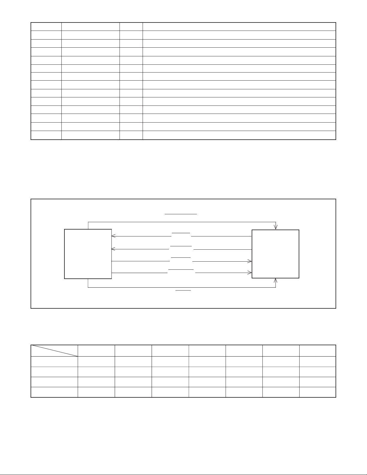
2. IC903 (CCD)
[Structure]
Interline type CCD image sensor
Optical size 1/2.5 type format
Effective pixels 2864 (H) X 2160 (V)
Pixels in total 2934 (H) X 2171 (V)
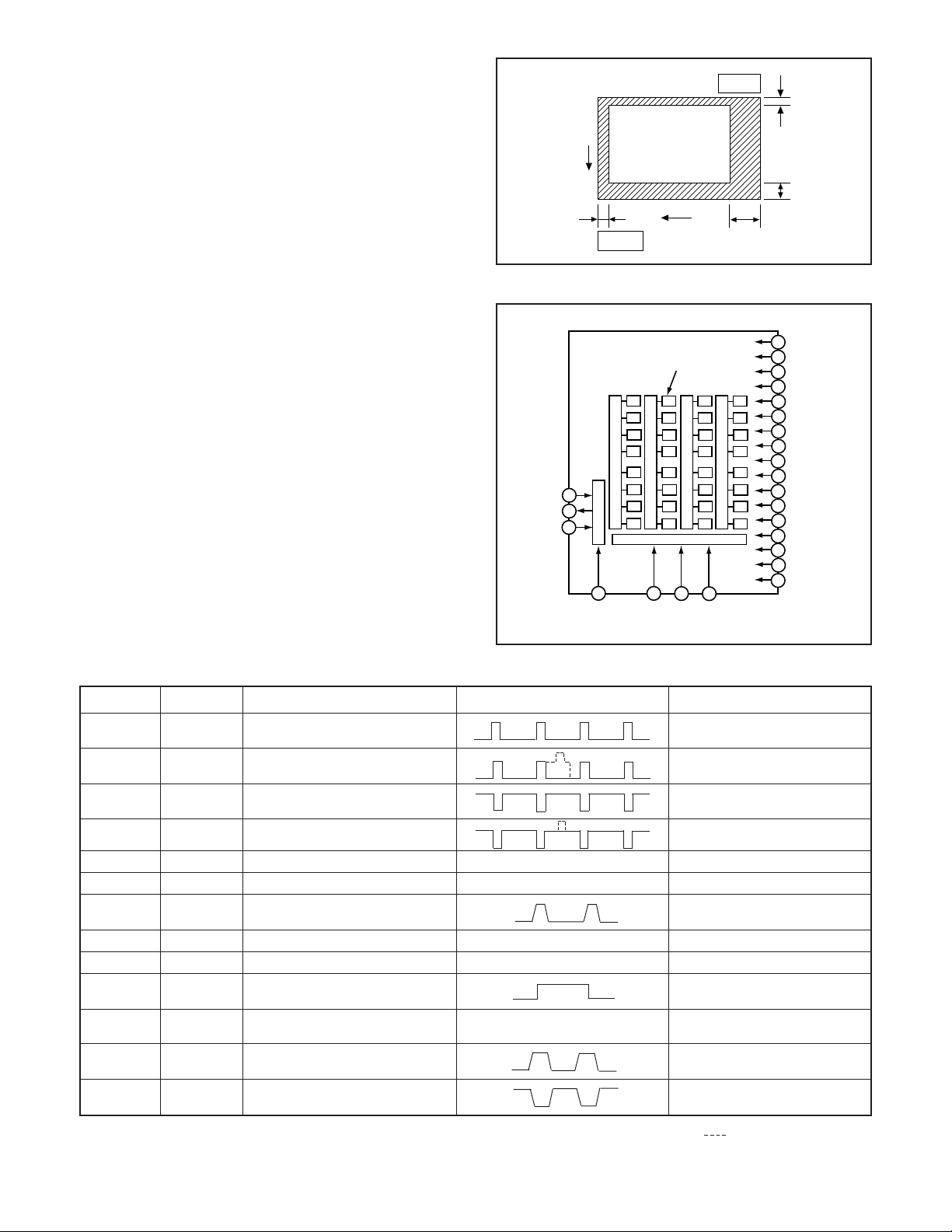
Optical black
Horizontal (H) direction: Front 12 pixels, Rear 58 pixels
Vertical (V) direction: Front 6 pixels, Rear 5 pixels
Dummy bit number Horizontal : 28 Vertical :7
Pin No.
Symbol Pin Description
Fig. 1-1.Optical Black Location (Top View)
Photo diode
10
VDD
VO
GND
13
14
15
Vertical shift register
Output part
Horizontal shift register
16
RG
ø
20
21
22
H2
H1
HL
ø
ø
ø
11
12
23
24
17
18
19
Fig. 1-2. CCD Block Diagram
Waveform
Voltag e
ø
1
ø
2
ø
3
ø
4
ø
5
ø
6
ø
7
ø
8
9
ø
ø
ø
GND
ø
ø
PT
SUBSW
ø
V6
V5B
V5A
V4
V3B
V3A
V3L
V3R
V2
V1
V1S
V5R
V5L
Vsub
1, 23, 24
2, 3
4, 7, 8, 9, 11
5, 6, 10
14
13
16
12, 15
17
18
19
20, 21
22
5L, V5R, V6
V
5A, V5B Vertical register transfer clock
V
V1S, V2, V3L,
V3R, V4
V
1, V3A, V3B
VO
VDD
ØRG
GND
PT
Vertical register transfer clock
Vertical register transfer clock
Vertical register transfer clock
Signal output
Circuit power DC 12 V
Reset gate clock
GND
Protection transister bias
Substrate controlSUB SW
SUB
L, H1
H
H
Substrate clock
Horizontal register transfer clock
Horizontal register transfer clock
2
Table 1-1. CCD Pin Description
-6.0 V, 0 V
-6.0 V, 0 V, 12 V
-6.0 V, 0 V
-6.0 V, 0 V, 12 V
DC
Aprox. 12 V
4.5 V, 7.8 V
GND 0 V
DC
-6.0 V
0, 3.3 V (When importing all
picture element: 3.3 V)
DC
Aprox. 6 V
(Different from every CCD)
0 V, 3.3 V
0 V, 3.3 V
When sensor read-out
– 3 –
Page 3

3. Part of IC905 (generation of vertical transfer clock,
H Driver) and IC901 (V Driver)
An H driver (part of IC905) and V driver (IC901) are necessary in order to generate the clocks (vertical transfer clock,
horizontal transfer clock and electronic shutter clock) which
driver the CCD.
IC905 has the generation of horizontal transfer clock and the
function of H driver, and is an inverter IC which drives the
horizontal CCDs (H1 and H2). It carries out generating vertical transfer clock, and output to IC901.
In addition the XV1-XV6 signals which are output from IC905
are vertical transfer clocks, and the XSG signal is superimposed onto XV1, XV3 and XV5 at IC901 in order to generate
a ternary pulse. In addition, the XSUB signal which is output
from IC101 is used as the sweep pulse for the electronic shutter, and the RG signal which is output from IC905 is the reset
gate clock.
4. IC905 (H Driver, CDS, AGC and A/D converter)
IC905 contains the functions of H driver, CDS, AGC and A/D
converter. As horizontal clock driver for CCD image sensor,
HØ1 (A and B) and HØ2 (A and B) are generated inside, and
output to CCD.
The video signal which is output from the CCD is input to pin
(A6) of IC905. There are sampling hold blocks generated from
the SHP and SHD pulses, and it is here that CDS (correlated
double sampling) is carried out.
After passing through the CDS circuit, the signal passes
through the AGC amplifier (VGA: Variable Gain Amplifier). It
is A/D converted internally into a 14-bit signal, and is then
input to ASIC (IC101). The gain of the VGA amplifier is controlled by pin (A2), (B3) and (C4) serial signal which is output
from ASIC (IC101).
REFB
REFT
OSUB
VM
OV1
RESET
SUBCNT
VDC
CH1
V5R
V5L
V3R
V3L
V1S
CLI
AD9996
14-BIT
ADC
CLAMP
INTERNAL
REGISTERS
CLO
14
DOUT
SL
SCK
SDI
VMSUB
9
3-level
10
VL
5
VL
27
2-level
24OV2
2-level
23OV4
2-level
21OV6
8
3-level
20
28
Level
1
conversion
3
Level
32
conversion
Level
V1
33
conversion
Level
31
V6
conversion
Level
V4
30
conversion
Level
29
V2
conversion
Level
37
conversion
Level
38
conversion
Level
35
conversion
Level
36
conversion
Level
34
conversion
2-level
2-level
2-level
2-level
2-level
3-level
3-level
3-level
3-level
Level
conversion
Level
conversion
Level
conversion
Level
conversion
Level
conversion
Level
conversion
Level
conversion
7
VHH
16
OV5R
15
OV5L
18
OV3R
17
OV3L
19
OV1S
25
VM
12
OV5A
11
OV5B
14
OV3A
13
OV3B
6
VH
26
VH
4
GND
41
CH2
40
V3
39
CH4
44
CH3
43
V5
42
CH5
2
SUB
CCDIN
3V INPUT
1.8V OUTPUT
1.8V INPUT
3V OUTPUT
H1 TO H8
XV1 TO XV24
XSUBCK
RG
HL
CDS
-3dB, 0dB, +3dB
LDO
REG
CHARGE
PUMP
HORIZONTAL
DRIVERS
8
24
VERTICAL
TIMING
CONTROL
8
GP01 TO GP08
Fig. 1-4. IC905 Block Diagram
6~42 dB
VGA
INTERNAL
CLOCKS
PRECISION
TIMING
GENERATOR
SYNC
GENERATOR
VD
HD
VREF
SYNC
Fig. 1-3. IC901 Block Diagram
– 4 –
Page 4

1-2. CP1, VF1 and TB1 CIRCUIT DESCRIPTION
1. Circuit Description
1-1. Digital clamp
The optical black section of the CCD extracts averaged values from the subsequent data to make the black level of the
CCD output data uniform for each line. The optical black section of the CCD averaged value for each line is taken as the
sum of the value for the previous line multiplied by the coefficient k and the value for the current line multiplied by the
coefficient 1-k.
1-2. Signal processor
1. γ correction circuit
This circuit performs (gamma) correction in order to maintain
a linear relationship between the light input to the camera
and the light output from the picture screen.
2. Color generation circuit
This circuit converts the CCD data into RGB signals.
3. Matrix circuit
This circuit generates the Y signals, R-Y signals and B-Y signals from the RGB signals.
4. Horizontal and vertical aperture circuit
This circuit is used gemerate the aperture signal.
1-3. AE/AWB and AF computing circuit
The AE/AWB carries out computation based on a 64-segment
screen, and the AF carries out computations based on a 6segment screen.
1-4. SDRAM controller
This circuit outputs address, RAS, CAS and AS data for controlling the SDRAM. It also refreshes the SDRAM.
1-5. Communication control
1. SIO
This is the interface for the 8-bit microprocessor.
2. PIO/PWM/SIO for LCD
8-bit parallel input and output makes it possible to switch between individual input/output and PWM input/output.
1-6. TG/SG
Timing generated for 6 million pixel horizontal addtion CCD
control.
1-7. Digital encorder
It generates chroma signal from color difference signal.
2. Outline of Operation
When the shutter opens, the reset signals (ASIC and CPU)
and the serial signals (“take a picture” commands) from the
8-bit microprocessor are input and operation starts.
When the TG/SG drives the CCD, picture data passes through
the A/D and CDS, and is then input to the ASIC as 10-bit
data. The AF, AE, AWB, shutter, and AGC value are computed from this data, and three exposures are made to obtain
the optimum picture. The data which has already been stored
in the SDRAM is read by the CPU and color generation is
carried out. Each pixel is interpolated from the surrounding
data as being either R, G, and B primary color data to produce R, G and B data. At this time, correction of the lens
distortion which is a characteristic of wide-angle lenses is
carried out. After AWB and γ processing are carried out, a
matrix is generated and aperture correction is carried out for
the Y signal, and the data is then compressed by JPEG and
is then written to card memory (SD card).
When the data is to be output to an external device, it is taken
data from the memory and output via the USB I/F. When played
back on the LCD and monitor, data is transferred from memery
to the SDRAM, and the image is then elongated so that it is
displayed over the SDRAM display area.
3. LCD Block
During EE, the YUV of 640 x 480 conversion is carried out for
the 12-bit RGB data which is input from the A/D conversion
block of the CCD to the ASIC in order to be displayed on the
video, and then transferred to the SDRAM.
The data which has accumulated in the SDRAM is converted
to digital YUV signal in conformity to ITUR-601 inside the ASIC
by SDRAM control circuit inside the ASIC, the data is sent to
the LCD driver IC and displayed the image to LCD panel after
gamma conversion is carried out.
If the shutter button is pressed in this condition, the 12-bit
data which is output from the A/D conversion block of the
CCD is sent to the SDRAM (DMA transfer), and is displayed
on the LCD as a freeze-frame image.
During playback, the JPEG image data which has accumulated in the SD card is converted to YUV signals. In the same
way as for EE, the data is then sent to the SDRAM, converted to digital YUV signal in conformity to ITUR-601 inside
the ASIC, the data is sent to the LCD driver IC and displayed
the image to LCD panel.
The LCD driver is converted digital YUV signals to RGB signals from ASIC, and these RGB signals and the control signal which is output by the LCD driver are used to drive the
LCD panel. The RGB signals are 1H transposed so that no
DC component is present in the LCD element, and the two
horizontal shift register clocks drive the horizontal shift registers inside the LCD panel so that the 1H/1V transposed RGB
signals are applied to the LCD panel.
Because the LCD closes more as the difference in potential
between the VCOM (common polar voltage: AC drive) and
the R, G and B signals becomes greater, the display becomes
darker; if the difference in potential is smaller, the element
opens and the LCD become brighter. In addition, the brightness and contrast settings for the LCD can be varied by means
of the serial data from the ASIC.
– 5 –
Page 5

4. Lens drive block
4-1. Focus drive
The focus motor is a stepping motor which is microstep-driven
by IC951. The 4 MHz clock signal (OSCIN) of the control signals (3-wire serial control (SDATA, SCLK, SENAB), VD) and
SUB CPU that are output from the ASIC (IC101) port is input
to IC951 so that IC951 can microstep control the focus motor.
Detection of the standard focusing motor position is carried
out by means of photointerruptor sensor inside the lens.
4-2. Zoom drive
The zoom motor is a stepping motor which is microstep-driven
by IC951. The 4 MHz clock signal (OSCIN) of the control signals (3-wire serial control (SDATA, SCLK, SENAB), VD) and
SUB CPU that are output from the ASIC (IC101) port is input
to IC951 so that IC951 can microstep control the zoom motor.
Detection of the standard zoom motor position is carried out
by means of photointerruptor sensor inside the lens.
4-3. ND filter
ND filter control is carried out by the control signals (ND ON
and ND OFF) that are output from the ASIC (IC101) port and
input to IC951 so that IC951 can drive the ND filter.
The 4 MHz clock signals (OSCIN) of the 3-wire serial control
signals (SDATA, SCLK, SENAB) and SUB CPU allow IC951 to
operate.
4-4. Iris drive
The drive method is a galvanometer type without braking coil.
The aperture opening amout is controlled as follows: the output from the Hall sensor inside the lens is amplified by the Hall
amplifier circuit inside the IC971 lens drive IC, and the difference between the current and target aperture determined by
the resulting output and the exposure amout output from the
ASIC (IC101) is input to the servo amplifier circuit (IC971) to
keep the aperture automatically controlled to the target aperture. The lens aperture control signal is output from IC971 and
is input to lens drive IN6B of IC951. IC951 functions as the
driver for driving the lens.
The 4 MHz clock signals (OSCIN) of the 3-wire serial control
signals (SDATA, SCLK, SENAB) and SUB CPU allow IC951 to
operate.
5. Video clip recording and playback
5-1. Recording
The signals from the camera block are input to the ASIC where
they are processed, and the image data that is stored in the
SDRAM built-in IC101 is input to the IC102 MPEG4 CODEC
LSI. The CODEC LSI converts this data to encoded MPEG4
data, after which it is returned to the ASIC as streaming data,
and the data is then written in sequence onto the SD card. At
this time, the audio signals that are input to the built-in microphone are converted into digital data by the audio CODEC IC
of IC181, and they are then input via the ASIC to IC102 (MPEG4
CODEC). The audio data is then encoded (AAC) by IC102,
and then it is returned to the ASIC as streaming data and is
then written in sequence onto the SD card together with the
image signals described above.
5-2. Playback
The data is read from the SD card and input to IC102 as streaming data. The encoded data is decoded into image data by
IC102 and then returned to the ASIC where it is displayed by
the LCD or on a TV monitor. At this time, the audio data is also
decoded by IC102, and it passes through the ASIC and is input to IC181 as digital data. D/A conversion is carried out at
IC181, and the sound is then output to the speaker or to the
LINE OUT terminal.
6. Audio CODEC circuit (IC181)
The audio signals from the microphone are converted into 16bit digital data. AD conversion is carried out at a maximum
sampling frequency of 48 kHz.
During audio playback, the 16-bit digital data is converted into
analog signals and these drive the speaker or line out system.
DA conversion is carried out at a maximum sampling frequency
of 48 kHz.
4-5. Shutter drive
Reverse voltage is applied to the above aperture coil to operate the shutter. With normal operation, the OC_EN and
OC_CONT signals that are output from the ASIC (IC101) are
maintained at a low level and when the shutter operates, the
OC_EN and OC_CONT signals switch to high, and after that
the SHUTTER + signal that is output from the ASIC (IC101)
becomes high and the shutter operates.
It is input to lens drive IN6B of IC951 with low level. IC951
functions as the driver for driving the lens.
The 4 MHz clock signals (OSCIN) of the 3-wire serial control
signals (SDATA, SCLK, SENAB) and SUB CPU allow IC951 to
operate.
– 6 –
Page 6

1-3. PWA and VF1 POWER CIRCUIT
DESCRIPTION
1. Outline (PWA)
This is the main power circuit, and is comprised of the following blocks.
Switching power controller (IC501)
Analog 12 V power output (Q5001, L5001)
Analog -6 V power output (Q5006, L5007)
Analog 3.4 V power output (IC503)
Digital 1.2 V power output (L5006)
Digital 3.25 V power output (L5005)
5 V system power output (L5004)
Digital 1.8 V power output (Q5004, L5014)
1-1. Switching Controller
This is the basic circuit which is necessary for controlling the
power supply for a PWM-type switching regulator, and is provided with six built-in channels, only CH1 (analog 12 V power
output), CH2 (analog -6 V power output), CH_M (digital 3.25
V power output), CH_SD (digital 1.2 V power output) and
CH_SU (5 V system power output) are used. Feedback from
12 V (A) (CH1), -6 V (A) (CH2), 3.25 V (D) (CH_M), 1.2 V (D)
(CH_SD) and 5 V (CH_SU) power supply outputs are received,
and the PWM duty is varied so that each one is maintained at
the correct voltage setting level.
1. Short-circuit Protection
If output is short-circuited for the length of time setting inside
IC501, all output is turned off. The control signal (P ON) are
recontrolled to restore output.
1-2. Analog 12 V Power Output
12 V (A) is output. Feedback for the 12 V (A) is provided to the
switching controller (Pin (3) of IC501) so that PWM control
can be carried out.
1-3. Analog -6 V Power Output
-6 V (A) is output. Feedback for the -6 V (A) is provided to the
switching controller (Pin (31) of IC501) so that PWM control
can be carried out.
1-4. Analog 3.4 V Power output
+3.4 V (A) is output. +3.4 V (A) is output which dropped 3.4 V
by 5V system power output at regulator IC503.
1-5. Digital 1.2 V Power Output
VDD1.2 is output. Feedback for the VDD1.2 is provided to the
switching controller (Pins (9) of IC501) so that PWM control
can be carried out.
1-6. Digital 3.25 V Power Output
VDD3 is output. Feedback for the VDD3 is provided to the
swiching controller (Pin (13) of IC501) so that PWM control
can be carried out.
1-7. 5 V System Power Output
+5 V is output. Feedback for the +5 V is provided to the
swiching controller (Pin (17) of IC501) so that PWM control
can be carried out.
1-8. Digital 1.8 V Power Output
VDD1.8 is output. Feedback for the VDD1.8 is provided to the
swiching controller (Pin (1) of IC501) so that PWM control
can be carried out.
1-9. Camera charging circuit
If the camera’s power is turned off, play mode and USB connection mode (card reader and pictbridge) setting while it is
connected to the AC adaptor, the battery will be recharged. In
the above condition, a CTL signal is sent from the microprocessor and recharging starts.
2. Outline (VF1)
This is the power circuit in the VF1 board, and is comprised
of the following blocks.
Backlight power output (IC514, Q5102, L5102)
2-1. Backlight Power Output
Regular current is being transmitted to LED for LCD backlight. Feedback for the voltage of R5124 and R5126 are provided to the controller (Pin (1) of IC514) so that PWM control
can be carried out.
– 7 –
Page 7

1-4. ST1 STROBE CIRCUIT DESCRIPTION
1. Charging Circuit
When UNREG power is supplied to the charge circuit and the
CHG signal from microprocessor becomes High (3.3 V), the
charging circuit starts operating and the main electorolytic
capacitor is charged with high-voltage direct current.
However, when the CHG signal is Low (0 V), the charging
circuit does not operate.
1-1. Charge switch
When the CHG signal switches to Hi, IC541 starts charging
operation.
1-2. Power supply filter
C5401 constitutes the power supply filter. They smooth out
ripples in the current which accompany the switching of the
oscillation transformer.
1-3. Oscillation circuit
This circuit generates an AC voltage (pulse) in order to increase the UNREG power supply voltage when drops in current occur. This circuit generates a drive pulse with a frequency
of approximately 150-250 kHz, and drive the oscillation transformer.
2. Light Emission Circuit
When FLCLT signal is input from the ASIC expansion port,
the stroboscope emits light.
2-1. Emission control circuit
When the FLCLT signal is input to the emission control circuit, Q5409 switches on and preparation is made to the light
emitting. Moreover, when a FLCLT signal becomes Lo, the
stroboscope stops emitting light.
2-2. Trigger circuit
The Q5409 is turned ON by the FLCLT signal and light emission preparation is preformed. Simultaneously, high voltage
pulses of several kV are emitted from the trigger coil and applied to the light emitter.
2-3. Light emitting element
When the high-voltage pulse form the trigger circuit is applied to the light emitting part, currnet flows to the light emitting element and light is emitted.
Beware of electric shocks.
1-4. Oscillation transformer
The low-voltage alternating current which is generated by the
oscillation control circuit is converted to a high-voltage alternating current by the oscillation transformer.
1-5. Rectifier circuit
The high-voltage alternating current which is generated at
the secondary side of T5401 is rectified to produce a highvoltage direct current and is accumulated at electrolytic capacitor C5412.
1-6. Charge monitoring circuit
The functions programmed in the IC541 monitor oscillations
and estimate the charging voltage. If the voltage exceeds the
rated value, charging automatically stops. Then, the CHGDONE signal is changed to Lo output and a "charging stopped"
signal is sent to the microcomputer.
– 8 –
Page 8

1-5. SYA CIRCUIT DESCRIPTION
1. Configuration and Functions
For the overall configuration of the SYA block, refer to the block diagram. The SYA block centers around a 8-bit microprocessor
(IC301), and controls camera system condition (mode).
The 8-bit microprocessor handles the following functions.
1. Operation key input, 2. Clock control and backup, 3. Power ON/OFF, 4. Storobe charge control.
Pin
1
2
3
4
5
6
7
8
9
10
11
12
13
14
15
16
17
18
19
20
21 LCD ON1
22 PLLEN
23 USB TRIG
24
25 CHG
26
27
28
29~34
35
36
37
38
39
40
41~44
45
46
47
48
49
50
Signal
SCLK
ZCARD
BACKUP CTL
BL ON
HOT LINE
TH ON
NOT USED
ZAV_JACK
VDD2
VSS2
VF. LED (R)
VF. LED (G)
CAM_LED
CHG_LED
BAT CHG ON
LENS_4M
MRST
TRST
ZUSB_DET
BAT CHG CTL
P ON
ZBOOT_COMREQ
FLW_SR
AVREF ON
SCAN IN5~0
VSS3
VDD3
FLW_SI
FLW_SCK
FLW_SO
DC_IN
SCAN OUT3~0
BAT CHG ERR
TIME OUT
BAT CHG I
BAT_TEMP
BAT_OFF
ZSREQ
I/O
O
O
O
O
O
O
O
O
O
O
O
O
O
O
O
O
O
O
O
I/O
Outline
Serial data clock
I
I
-
I
-
-
I
I
I
I
I
-
-
I
I
I
I
I
I
I
I
I
SD card detection (L= card)
Backup battery charge control (L= charge)
LCD backlight control (H= ON)
Hot line from ASIC
Temperature sensor power ON/OFF (L= ON)
-
AV jack detection (L= AV jack detection)
Backup 3.2 V
GND
VF. LED (red) (H= lighting)
VF. LED (green) (H= lighting)
Cradle camera detection display LED drive (L= lighting)
Cradle charging display LED drive (L= lighting)
Start charging (H= start)
Lens driver 4M clock output
System reset output (L= reset)
T reset output (L= reset)
USB detection input (L= USB detection)
Charge current control
LCD start-up signal output (H= start up)
PLL ON/OFF control (H=ON)
Cradle USB trigger detection (H= trigger detection)
D/D converter ON/OFF control (H= ON)
Strobo condensor charge control signal (H= charge)
Boot/command request input from ASIC
FLW_SR Flash writer
SW 3.2 V ON/OFF control (L= ON)
Keyscan input 5~0
GND
Backup 3.2 V
FLW_SI Flash writer
FLW_SCK Flash writer
FLW_SO Flash writer
DC power connection detection input (L= DC power detection)
Keyscan output 3~0
IC524 Fault output detection (L= fault detection)
IC524 CHRG output detection (L= TIME OUT detection)
IC524 Charge current monitoring (AD conversion input)
Lithum ion battery temperature detection (AD conversion input)
Battery OFF detection signal input (L= OFF detection)
Transmission clock for communication (SYA ↔ ASIC)
See next page →
– 9 –
Page 9
51 SCAN IN6
52
53
54
55
56
57
58
59
60
61
62
63
64
IR_IN
RESET
XCIN
XCOUT
VSS1
XIN
XOUT
VDD1
BATTERY I
CHG_DONE I Strobo condensor charging completion signal input (H= charging completion)
INT_TEMP
ASIC SI
ASIC SO
I
I Cradle infrared remote control transmission data (asynchronous) input
I
I
O
-
I
O
-
I
O Serial data output to ASIC
I Serial data input to ASIC
Table 5-1. 8-bit Microprocessor Port Specification
Keyscan input 6
Reset input
Clock (32.768 KHz)
Clock
GND
Main clock (4MHz)
Main clock
Backup 3.2 V
UNREG SY voltage measurement input
Substrate temperature measurement input around ASIC (AD convertion input)
2. Internal Communication Bus
The SYA block carries out overall control of camera operation by detecting the input from the keyboard and the condition of the
camera circuits. The 8-bit microprocessor reads the signals from each sensor element as input data and outputs this data to the
camera circuits (ASIC) or to the LCD display device as operation mode setting data. Fig. 5-1 shows the internal communication
between the 8-bit microprocessor, ASIC and SPARC lite circuits.
ASIC RESET
S. REQ
8-bit
Microprocessor
Fig. 5-1 Internal Bus Communication System
ASIC SO
ASIC SI
ASIC SCK
MRST
3. Key Operaiton
For details of the key operation, refer to the instruction manual.
SCAN
OUT
SCAN
IN
0
1
0
← LEFT
TELE
2
3
-
1
→ RIGHT
WIDE
--
TEST
2
↑ UP
REC
PLAY
-
3
↓ DOWN
1st SHUTTER
-
-
4
SET
2nd SHUTTER
-
-
ASIC
5
MENU
CAMERA
-
-
6
LCD LOTATION
PLAY
POWER ON
PANEL OPEN
Table 5-2. Key Operation
– 10 –
Page 10

4. Power Supply Control
The 8-bit microprocessor controls the power supply for the overall system.
The following is a description of how the power supply is turned on and off. When the battery is attached, a regulated 3.2 V
voltage is normally input to the 8-bit microprocessor (IC301) by IC303, so that clock counting and key scanning is carried out
even when the power switch is turned off, so that the camera can start up again. When the battery is removed, the 8-bit microprocessor operates in sleep mode using the backup lithum battery. At this time, the 8-bit microprocessor only carries out clock
counting, and waits in standby for the battery to be attached again. When a switch is operated, the 8-bit microprocessor supplies
power to the system as required.
The 8-bit microprocessor first sets the P ON signal at pin (24) to high, and then turns on the DC/DC converter. After this, low
signal is output from pin (17) so that the ASIC is set to the reset condition. After this these pins set to high, and set to active
condition. If the LCD monitor is on, the LCD ON 1 signal at pin (21) set to high, and the DC/DC converter for the LCD monitor is
turned on. Once it is completed, the ASIC returns to the reset condition, all DC/DC converters are turned off and the power
supply to the whole system is halted.
ASIC,
memory
Power voltage
Power OFF
Power switch ON-
Auto power OFF
CAMERA
LCD finder
Play back
Table 5-3. Camera Mode
Note) 4 MHz = Main clock operation, 32 kHz = Sub clock operation
3.3 V 1.2 V
OFF
OFF
ON
ON
CCD
5 V (A)
+12 V etc.
OFF
OFF
ON
OFF
8 bit
CPU
3.2 V
(ALWAYS)
32KHz OFF
32KHz OFF
4 MHz ON
4 MHz ON
MONITOR
5 V (L) etc.
LCD
– 11 –
Page 11
2. DISASSEMBLY
2-1. REMOVAL OF CABINET LEFT, CP1 BOARD AND TB1 BOARD
1. Open the cover battery.
2. Screw 1.7 x 3
3. Screw 1.7 x 4.5
4. Two screws 1.7 x 3
5. Four screws 1.7 x 5
6. Cabinet left
7. Two screws 1.7 x 4
8. Screw 1.7 x 3
9. Screw 1.7 x 4
10. Connector
11. Holder speaker
12. FPC
9
10
8
4
11
16
12
13. Flexible FPC
14. Connector
15. CP1 board
16. Connector
17. Screw 1.7 x 4
18. Dec grip front
19. Two FPCs
20. Screw 1.7 x 3
14
21
21. Screw 1.7 x 4
22. Assy wire VF1 & TB1
23. TB1 board
24. Screw 1.7 x 4
25. Stand
1
19
22
A
23
2
13
3
A
20
24
25
7
6
5
17
18
15
5
– 12 –
Page 12

2-2. REMOVAL OF FRONT ASSY, ST1 BOARD AND CA1 BOARD
1. Assy lens
2. Front assy
3. Screw 1.7 x 4
4. Flexible PWB
5. Spacer B
6. Remove the solder.
7. ST1 board
8. Three screws 1.4 x 3.5
9. CA1 board
10. Unit control
10
9
a
b
c
8
When assembling,
tighten the screws order.
a → b → c
NOTE: Discharge a strobe capacitor
with the discharge jig (VJ8-0188) for
electric shock prevention.
1
3
4
7
2
6
5
black
red
gray
– 13 –
Page 13

2-3. REMOVAL OF CABINET RIGHT, LCD AND VF1 BOARD
15
18
20
24
16
25
13
19
23
17
10
22
1. Button power
2. Two screws 1.7 x 2.5
3. Spring button
4. Button LCD
5. Screw 1.7 x 3
6. Cover joint base
7. Screw 1.7 x 2.5
8. Holder joint
9. Cabinet right
7
8
1
10. Four screws 1.4 x 2.5
11. Cover LCD back
12. Assy wire VF1 & TB1
13. Assy wire VF1 & CP1
14. Unit sw FPC
2
4
3
12
27
26
14
21
11
10
6
5
15. Cover LCD front
16. FPC
17. Remove the solder.
18. LCD
19. Holder monitor
9
20. Two screws 1.7 x 2.5
21. Holder mic
22. Two microphones
23. VF1 board
24. Two screws 1.7 x 2
25. Assy joint
26. Screw 1.4 x 2
27. Unit sw FPC
– 14 –
Page 14
2-4. BOARD LOCATION
CA1 board VF1 board
CP1 board
ST1 board
TB1 board
– 15 –
Page 15

3. ELECTRICAL ADJUSTMENT
3-1. Table for Servicing Tools
Ref. No.
J-1
J-2
J-3
J-4
J-5
J-6
Name
Pattern box (color viewer)
Calibration software
Chroma meter
Spare lump
Discharge jig
Collimator
Number
1
1
1
1
1
1
Part code
VJ8-0190
VJ8-0263
VJ8-0192
VJ8-0191
VJ8-0188
VJ8-0260
3-4. Setup
1. System requirements
Windows 98 or Me or 2000 or XP
IBM R -compatible PC with pentium processor
CD-ROM drive
3.5-inch high-density diskette drive
USB port
40 MB RAM
Hard disk drive with at least 15 MB available
VGA or SVGA monitor with at least 256-color display
Note: J-1 Pattern box (color viewer) is 100 - 110 VAC only.
J-1 J-2
J-3
J-4
J-5
3-2. Equipment
1. Oscilloscope
2. Digital voltmeter
3. AC adaptor
4. PC (IBM R -compatible PC, Pentium processor, Window
98 or Me or 2000 or XP)
2. Installing calibration software
1. Insert the calibration software installation diskette into your
diskette drive.
2. Open the explorer.
3. Copy the DscCalDI_150 folder on the floppy disk in the FD
drive to a folder on the hard disk.
3. Installing USB driver
Install the USB driver with camera or connection kit for PC.
4. Pattern box (color viewer)
Turn on the switch and wait for 30 minutes for aging to take
place before using Color Pure. It is used after adjusting the
chroma meter (VJ8-0192) adjust color temperature to 3100 ±
20 K and luminosity to 900 ± 20 cd/m
2
. Be careful of handling
the lump and its circumference are high temperature during
use and after power off for a while.
5. Computer screen during adjustment
Calibration
AWB
Focus
UV Matrix
Cal Mode
Cal Data
USB storage
VID
Get
PID
Set
Backrush pulse :
OK
OK
Upload
Firmware
Data
PAF Cal.
EVF
LCD Type
Get
LCD
RGB Odd
RGB Gain
Tint
VCO
H AFC Test
Serial
Set
Set
Rev.
RGB Even
VCOMDC
Phase
Set
Set
Set
VCOMPP(LOW)
VCOMPP(HI)
Hall Cal.
Setting
Language
Video Mode
Factory Code
3-3. Adjustment Items and Order
1. IC501 Oscillation Frequency Adjustment
2. Lens Adjustment
3. AWB Adjustment
4. CCD White Point Defect Detect Adjustment
5. CCD Black Point And White Point Defect Detect Adjustment In Lighted
Note: Item 2-5 adjustments should be carried out in sequence.
– 16 –
Page 16

3-5. Connecting the camera to the computer
1. Line up the arrow on the cable connector with the notch on the camera's USB port. Insert the connector.
2. Locate a USB port on your computer.
3. Insert the AC adaptor’s cable to DC jack.
4. If “USB CONNECTION” is displayed, choose the “CARD READER”, and press the SET button.
NOTE: Discharge a strobe capacitor
with the discharge jig (VJ8-0188) for
electric shock prevention.
AC adaptor
USB cable
To USB port
– 17 –
Page 17

3-6. The adjustment item which in necessary in part exchange
CCD Black
Point And White
Point Defect
Detect
Adjustment In
Lighted
Factory
Cord
Setting
Language
Setting
COMPL PWB CP-1
(636 092 2068)
COMPL PWB TB-1
(636 092 2082)
COMPL PWB ST-1
(636 092 2129)
COMPL PWB VF-1
(636 092 2150)
COMPL PWB CA-1
(636 091 5640)
LENS ASSY
(636 072 1205)
IC501
Oscillation
Frequency
Adjustment
Lens
Adjustment
AWB
Adjustment
CCD White
Point Defect
Detect
Adjustment
: Be sure to carry out the necessary adjustments after replacing the unit.
: Adjustment is possible from the menu setting screen of the camera and by using the calibration software.
3-7. Adjust Specifications
[CP1 board (Side B)]
Adjustment method:
1. Adjust with VR501 to 796.5 ± 1 kHz.
2. Lens Adjustment
USB storage
information
registration
Reset
Setting
CL501
VR501
Note:
1. Frequency adjustment is necessary to repair in the CP1
board and replace the parts.
Preparation:
1. Remove the cabinet left. You can see VR501 and CL501
in the CP1 board.
2. Insert the SD card.
3. Set the main switch to the REC.
4. Press the power button, and comfirm that the through image from CCD can be seen in the LCD.
1. IC501 Oscillation Frequency Adjustment
Measuring Point
Measuring Equipment
ADJ. Location
ADJ. Value
CL501
Frequency counter
VR501
796.5 ± 1 kHz
Camera
Collimator
Preparation:
POWER switch: ON
If using a ready-made collimator, set to infinity.
Note:
Do not vibrate during the adjustment.
Adjustment method:
1. Set the camera 0 cm from the collimator. (Do not enter any
light.)
2. Set the camera so that it becomes center of the screen in
the collimator.
3. Double-click on the DscCalDi.exe.
4. Click the Focus, and click the Yes.
5. Lens adjustment value will appear on the screen.
6. Click the OK.
– 18 –
Page 18

DscCalDi
x
Dsc Calibration x
Focus Result
!
STD_AFPOS=1896
FOCUS=-4,0,-9,-116
ADJ_PZPOS=15
OK
Adjustment value determination is effectuated using the "STD
AFPOS" and "FOCUS" values.
If FOCUS=focus1, focus2, focus3, focus4 and the adjustment
values fulfill the conditions below, they are determined as within
specifications.
Adjustment value determination
1800<=STD_AFPOS<2000
-40<=focus1<=+40, -50<focus2<+50,
-60<=focus3<=+60, -200<=focus4<=+200
3. AWB Adjustment
Camera
Pattern box
(color viewer)
AWB Result:
1:
AGC=187,356,525,694,863
3F_AGC=1,2
WB=276,516,678
CHECK=128,128,141
WB_ND=275, 515, 691
CHECK_ND=128, 128, 142
IRIS_GAIN: 52
IRIS_OFFSET: 153
MS=1705,2101,2378,2934
IRIS=171,156,137,116,109
0
IRIS=0
Adjustment value determination is effectuated using the "AGC",
“CHECK", “CHECK_ND”, "MS", “IRIS”, “IRIS_GAIN” and
“IRIS_OFFSET” values.
If AGC= a1, a2, a3, a4, a5, CHECK= wc0, wc1, wc2,
CHECK_ND= wnc0, wnc1, wnc2, MS= ms1, ms2, ms3, ms4,
IRIS= s1, s2, s3, s4, s5, IRIS_GAIN= g and IRIS_OFFSET=
o the adjustment values fulfill the conditions below, they are
determined as within specifications.
Adjustment value determination
50<a1<310, 100<a2<550, 200<a3<750,
300<a4<950, 400<a5<1024
wc0=128 ± 2, wc1=128 ± 2, wc2=130 ± 40
wnc0=128 ± 2, wnc1=128 ± 2, wnc2=130 ± 40
1400<ms1<=2500, 1700<ms2<=2900, 1800<ms3<=3100,
2300<ms4<=3600
100<=s1<=220, 100<=s2<=220, 100<=s3<=220,
100<=s4<=220, 100<=s5<=220
s1>s2>s3>s4>s5
0<=g<=255
0<=o<=255
Adjustment values other than the above are irrelevant.
OK
Copy
Preparation:
POWER switch: ON
Adjusting method:
1. When setting the camera in place, set it to an angle so that
nothing appears in any part of the color viewer except the
white section. (Do not enter any light.)
2. Double-click on the DscCalDi.exe.
3. Click the AWB, and click the Yes.
4. AWB adjustment value will appear on the screen.
5. Click the OK.
4. CCD White Point Defect Detect Adjustment
Preparation:
POWER switch: ON
Adjustment method:
1. Double-click on the DscCalDi.exe.
2. Select “CCD Defect” on the LCD “Test”, and click the “Ye s ”.
3. After the adjustment is completed, OK will display.
4. Click the OK.
– 19 –
Page 19

5. CCD Black Point And White Point Defect Detect
Adjustment In Lighted
Camera
Pattern box
(color viewer)
Preparation:
POWER switch: ON
Setting of pattern box:
Color temperature: 3100 ± 20 (K)
Luminance: 900 ± 20 (cd/m
Adjusting method:
1. Set the camera 0 cm from the pattern box. (Do not enter
any light.)
2. Double-click on the DscCalDi.exe.
3. Select “CCD Black” on the LCD “Test”, and click the “Ye s ”.
4. After the adjustment is completed, the number of defect
will appear.
2
)
3-8. Factory Code Setting
1. Check the "Factory Code" display within the Setting group.
2. For U.S.A., Canada and NTSC general area
If "FC_SANYO_U" does not appear, click on the " " mark
located on the right of the "Factory Code" display BOX and
select "FC_SANYO_U".
3. For Europe and PAL general area
If "FC_SANYO_EX" does not appear, click on the " " mark
located on the right of the "Factory Code" display BOX and
select "FC_SANYO_EX".
3-9. Language Setting
1. Click on the " " mark located on the right of the
"Language" display BOX.
2. Select language. (Default is English.)
3. End "DscCal" and remove the camera before turning the
camera power OFF.
Calibration
AWB
Focus
UV Matrix
Cal Mode
Cal Data
USB storage
VID
Get
PID
Set
Backrush pulse :
OK
OK
Upload
Firmware
Data
PAF Cal.
EVF
LCD Type
Get
LCD
RGB Odd
RGB Gain
Tint
VCO
H AFC Test
Serial
Set
Set
Rev.
RGB Even
VCOMDC
Phase
Set
Set
Set
VCOMPP(LOW)
VCOMPP(HI)
Hall Cal.
Setting
Language
Video Mode
Factory Code
3-10. Reset Setting
Carry out reset settings after replacing CP1 board.
1. Turn on the camera.
2. Press the MENU button.
3. Choose the OPTION.
4. Choose the RESET SETTINGS, and press the SET
button.
5. Select Yes, and press the SET button.
3-11. The Compulsive boot starting method
1. Keep MENU button, SET button, and SHUTTER button depressed while switching on the power.
2. Connect the camera and the computer with USB cable.
– 20 –
Page 20

3-12. Firmware uploading procedure
1. Uploading the firmware should be carried out if the version
number (COMPL PWB XX-X) on the replacement circuit
board is lower than the version of the distributed firmware.
For XX-X, enter the name of the circuit board containing the
firmware.
2. The firmware is distributed by e-mail in self-extracting archive
format. Change the extension of the distributed file to .EXE
and save it in your preferred folder.
3. When you double-click the saved file, the firmware (binary
file) will be saved in the same folder.
4. The firmware must not be distributed without permission.
1. Overwriting firmware from the SD card
Preparation:
SD card: SD card with firmware rewritten into the root directory
Data: S815Nxxx.BIN (xxx: version)
Overwriting method:
1. Insert the above SD card.
2. Turn on the camera.
3. Set the main switch to the PLAY.
4. Press the MENU button. The playback setting screen appears.
5. Choose the OPTION icon.
6. Choose the FORMAT.
7. Toggle the SET button to the left for 2 seconds. FIRMWARE
UPDATE will display.
8. Choose YES.
9. Press the SET button. Update is starting.
Note:
Do not turn off the camera’s power or remove the SD card
while the firmware is being updated.
The power will turn on automatically after the update is complete.
2. Overwriting firmware from the calibration software
Preparation:
PC with overwriting firmware copied to the preferred folder in
the HD.
Data: S815Nxxx.BIN (xxx: version)
Overwriting method:
1. Connect the camera’s USB/AV terminal to the computer’
USB connector.
2. The USB Connection screen appears on the camera’s LCD
monitor. Choose the “CARD READER”, and press the SET
button.
3. Double-click on the DscCalDi.exe.
4. Click the Firmware.
5. Choose the fimware file to use for overwriting, and click
the Yes.
6. Update is starting. The message will appear, and choose
OK.
7. After the update is complete, disconnect the USB cable
and turn the camera’s power off.
Note:
Do not turn off the camera’s power while the firmware is being updated.
– 21 –
Page 21

4. USB STORAGE INFORMATION
REGISTRATION
USB storage data is important for when the camera is connected to a computer via a USB connection.
If there are any errors in the USB storage data, or if it has not
been saved, the USB specification conditions will not be satisfied, so always check and save the USB storage data.
Preparation:
POWER switch: ON
Adjustment method:
1. Connect the camera to a computer. (Refer to 3-5. Con-
necting the camera to the computer on the page 17.)
2. Double-click on the DscCalDi.exe.
3. Click on the Get button in the USB storage window and
check the USB storage data.
VID: SANYO
PID: C6
Serial:
Rev. : 1.00
4. Check the “Serial” in the above USB storage data. If the
displayed value is different from the serial number printed
on the base of the camera, enter the number on the base
of the camera. Then click the Set button.
5. Next, check VID, PID and Rev. entries in the USB storage
data. If any of them are different from the values in 3. above,
make the changes and then click the corresponding Set
button.
Calibration
AWB
Focus
UV Matrix
Cal Mode
Cal Data
USB storage
VID
Get
PID
Set
Backrush pulse :
OK
OK
Upload
Firmware
Data
PAF Cal.
EVF
LCD Type
Get
LCD
RGB Odd
RGB Gain
Tint
VCO
H AFC Test
Serial
Set
Set
Rev.
RGB Even
VCOMDC
Phase
Set
Set
Set
VCOMPP(LOW)
VCOMPP(HI)
Hall Cal.
Setting
Language
Video Mode
Factory Code
– 22 –
Page 22

5. TROUBLESHOOTING GUIDE
POWER LOSS INOPERTIVE
PUSH THE POWER
SW FOR A WHILE
IC301-43
(SCAN OUT2)
PULSE INPUT
NO
IC303-7 5.3 V
(BOOST 5.3 V)
YES
IC301-3, 9, 36, 59
(VDD)
HIGH
IC301-53
(RESET)
HIGH
IC301-49
(BAT OFF)
HIGH
IC301-58
OSCILLATION
YES
IC301-55
OSCILLATION
YES
YES
NO
CHECK S3102
CHECK TB1, IC955,
LOW
LOW
CHECK IC302, RB302
LOW
NO
NO
CHECK RB302
CHECK X3001
CHECK X3002
Q9562
CHECK IC302
TAKING INOPERATIVE
PUSH SHUTTER
BUTTON
IC301-30, 31
(SCAN IN 3, 4)
PULSE INPUT
YES
IC501-18, 29
(P ON, PA ON)
IC503-1 (PA ON3)
HIGH
SERIAL
COMMUNICATION
OK
CHECK CP1 DMA
BLOCK
NO
CONTROL PANEL,
LOW
CHECK IC101, IC301,
NG
CP1 DMA BLOCK
CHECK UNIT
D3112, D3111
PWA BLOCK
CHECK IC301,
CHECK IC301
NO PICTURE
IC101-264
CHECK
OSCILLATION
OK
IC301-64, 63
(ASIC_SO, ASIC_SI)
OK
CHECK SOLDERING
OF MEMORY
EACH PIN
MAIN CLOCK FOR SYSTEM OPERATION
NG
NO OPERATION IF ABSENT
CHECK X1102 OSCILLATOR
INCORRECT HANDSHAKING
NG
BETWEEN 8-BIT CPU AND ASIC
CHECK EACH INTERFACE
– 23 –
Page 23

6. PARTS LIST
ACCESSOEIES
LOCATION PARTS NO. DESCRIPTION LOCATION PARTS NO. DESCRIPTION
Note: Refer to table 6-1.
1 636 087 0017 STRAP -SX719/U
2 636 093 8458 CASE SOFT-SX815/J
3 636 087 4398 ASSY,CAP LENS-SX719/J,
VPC-C6EXBK, VPC-C6EXR
3 636 092 0842 ASSY,CAP LENS-SX815/J,
EXCEPT VPC-C6EXR, VPC-C6EXBK
4 645 083 4240 ADAPTOR,DOCKING STATION,
EXCEPT VPC-C6E, VPC-C6EXE
4 645 081 9988 ADAPTOR,DOCKING STATION,
VPC-C6E, VPC-C6EXE
5 645 084 9398 CABLE,DSC A/V-SX815/J
6 645 023 4958 CORE,CLUMP (Core for the cable of USB),
VPC-C6 ONLY
7 645 075 2087 CABLE,DSC USB,SX719
8 645 079 8160 REMOCON,INFRARED,
EXCEPT VPC-C6, VPC-C6EX
8 645 075 2070 REMOCON,INFRARED, VPC-C6, VPC-C6EX
9 645 057 1503 CORD,POWER-1.2MK,
EXCEPT VPC-C6, VPC-C6E
9 645 080 8876 CORD,POWER-1.2MK, VPC-C6E ONLY
9 645 036 7434 CORD,POWER-1.2MK, VPC-C6E ONLY
9 645 076 0235 CORD,POWER-1.5MK,
EXCEPT VPC-C6, VPC-C6E
9 645 076 0228 CORD,POWER-1.5MK, VPC-C6 ONLY
10 645 080 1846 ADAPTOR,AC-DC
11 645 081 9995 ADAPTOR,CABLE-SX815
12 645 063 5816 BATTERY,RECHARGE,LI-ION
13 645 081 9865 DISC,CD-ROM SSP 815 U(DISK 2) (N.S.P.)
(SANYO softwerae pack)
13 645 081 9858 DISC,CD-ROM SSP 815 U1(DISK 1) (N.S.P.)
(SANYO softwerae pack),
( INSTRUCTION MANUAL: English, German,
French, Spanish, Itlian, Dutch, Russia, Chineese)
PACKING MATERIALS
7001 636 092 3287 CARTON INNER-SX815/EX,
EXCEPT VPC-C6, VPC-C6EXE
7001 636 093 8465 CARTON INNER-SX815/EX4, VPC-C6EXE ONLY
7001 636 092 3270 CARTON INNER-SX815/U, VPC-C6 ONLY
7002 636 078 4659 CUSHION SHEET-SX792/KRNK
7003 636 094 2165 LABEL BLACK MODEL-815/EX3(TOP),
VPC-C6EXBK ONLY
7003 636 094 2141 LABEL RED MODEL-SX815/EX2(TOP),
VPC-C6EXR ONLY
7004 636 073 2087 LABEL CARTON BLACK 711EX2(SIDE),
VPC-C6EXBK ONLY
7004 636 094 2158 LABEL CARTON RED-815/EX2(SIDE),
VPC-C6EXR ONLY
7005 636 092 3324 REINFORCE PAD-815/J (TOP)
7006 636 092 3317 REINFORCE PAD,A-815/J (BOTTOM)
9053 636 092 1801 INSTRUCTION MANUAL (CAMERA, SOFTWARE)
(English)
24
Page 24

12
34
5
8
11
12
7
6
9
10
13
6-1. Table of accessories
25
Page 25

CABINET AND CHASSIS PARTS 1
LOCATION PARTS NO. DESCRIPTION LOCATION PARTS NO. DESCRIPTION
1 636 092 0682 CABINET LEFT-SX815/J,
EXCEPT VPC-C6EXR, VPC-C6EXBK
1 636 092 9289 CABINET LEFT-SX815/J2, VPC-C6EXR
1 636 092 9470 CABINET LEFT-SX815/J3, VPC-C6EXBK
2 636 092 0811 DEC GRIP FRONT-SX815/J,
EXCEPT VPC-C6EXR, VPC-C6EXBK
2 636 092 9432 DEC GRIP FRONT-SX815/J2,
VPC-C6EXR, VPC-C6EXBK
3 636 089 5249 LABEL WEEE -SX719/EX, VPC-C6E, VPC-C6EXE
4 636 083 0059 COVER SPEAKER-SX719/J, VPC-C6EXBK ONLY
4 636 086 3460 COVER SPEAKER-SX719/J2,
EXCEPT VPC-C6EXBK
5 636 083 0004 ADHESIVE COVER SP-SX719/J
6 636 092 0712 HOLDER STRAP-SX815/J
7 636 083 0424 SPACER LENZ LEFT-SX719/J
8 636 083 0271 HOLDER STRAP INNER-SX719
9 636 093 2692 SPACER CABI LEFT-SX815/J
10 636 082 5093 FLEXIBLE PWB SX719ST1-CP1
11 636 092 2129 COMPL PWB,ST-1
12 636 072 3559 SPACER F CON-SX613/J
13 636 083 0158 DEC FRONT-SX719/J,
EXCEPT VPC-C6EXR, VPC-C6EXBK
13 636 092 0798 DEC FRONT-SX815/J2,
VPC-C6EXR, VPC-C6EXBK
14 636 092 0781 CABINET FRONT-SX815/J,
EXCEPT VPC-C6EXR, VPC-C6EXBK
14 636 092 9401 CABINET FRONT-SX815/J2,
VPC-C6EXR VPC-C6EXBK
15 636 083 0172 DEC FLASH-SX719/J
16 645 075 0939 ASSY,LAMP-SX719
17 636 086 1336 SPACER FLASH-SX719/J
18 636 094 8860 CABI FRONT INNER-SX815/J
19 636 083 0240 HOLDER CABI FRONT-SX719/J
20 636 084 7361 SPACER FRONT INNER-SX719
21 636 094 3674 SPACER B-SX815/J
22 645 041 3131 PAD(L=9)
23 636 094 5975 SPACER C-SX815/J
24 645 072 1779 SPEAKER,8
25 636 083 0301 HOLDER SPEAKER-SX719/J
26 636 083 1063 SPACER SPEAKER-SX719/J
27 636 092 5113 COMPL PWB,CP-1(F/W)
28 636 094 5791 SPACER_CP1SL_SX815
29 636 094 5814 SHIELD_TAPE_CP1_SX815
30 636 083 0349 SPACER CP1-SX719/J
31 636 092 2082 COMPL PWB,TB-1
32 636 092 0521 SPACER TB1-SX815/J
33 636 092 0576 STAND-SX815/J,
EXCEPT VPC-C6EXR, VPC-C6EXBK
33 636 092 9296 STAND-SX815/J2, VPC-C6EXR ONLY
33 636 092 9487 STAND-SX815/J3, VPC-C6EXBK ONLY
34 645 072 1205 LENS(ASSY)
35 645 081 9964 OPTICAL FILTER
36 636 082 8131 SPACER SX719
37 636 092 3782 COMPL PWB,CA-1 SV-SX815
38 636 086 1374 SPACER CA1-SX719/J
39 645 081 7021 UNIT,CONTROL-SX815/J,
EXCEPT VPC-C6EXR, VPC-C6EXBK
39 645 083 4288 UNIT,CONTROL-SX815/J2,
VPC-C6EXR, VPC-C6EXBK
40 636 094 5807 SPACER_TB1B_SX815
101 412 067 5407 SP SCR HMPN1.7X5A NEW-R,
EXCEPT VPC-C6EXR, VPC-C6EXBK
101 412 070 1502 SP SCR HMPN1.7X5WP NEW-R,
VPC-C6EXR, VPC-C6EXBK
102 411 178 9403 SCR S-TPG PAN PCS 1.7X4.0
103 411 182 4609 SCR PAN PCS 1.7X4.5,
EXCEPT VPC-C6EXR, VPC-C6EXBK
103 411 194 8305 SCR PAN PCS 1.7X4.5, VPC-C6EXR, VPC-C6EXBK
104 411 175 5705 SCR PAN PCS 1.7X3,
EXCEPT VPC-C6EXR, VPC-C6EXBK
104 411 194 8206 SCR PAN PCS 1.7X3, VPC-C6EXR, VPC-C6EXBK
105 412 064 3604 SPECIAL SCREW-1.7X2.5
106 411 177 6502 SCR S-TPG PAN PCS 1.7X4
107 411 018 0805 SCR PAN PCS 1.7X2
108 411 175 5705 SCR PAN PCS 1.7X3
109 412 071 1105 SPECIAL SCREW-1.7X3,
VPC-C6EXBK, VPC-C6EXR
109 412 060 7903 SPECIAL SCREW-1.7X3.0,
EXCEPT VPC-C6EXR, VPC-C6EXBK
110 411 181 8707 SCR S-TPG PAN PCS 1.4X3.5
26
Page 26

CABINET & CHASSIS PARTS 1
37
110
102
39
25
38
26
27
28
36
35
29
102
34
108
109
32
24
6
5
22
4
102
103
5
23
3
108
1
102
104
7
102
30
107
9
8
40
2021
105
101
2
10
19
106
31
18
17
33
102
14
13
16
15
12
11
SX815/J Parts List1
101
101
27
Page 27

CABINET AND CHASSIS PARTS 2
LOCATION PARTS NO. DESCRIPTION LOCATION PARTS NO. DESCRIPTION
1 636 092 9319 ASSY,BUTTON POWER-815/J2,
VPC-C6EXR ONLY
1 636 092 9494 ASSY,BUTTON POWER-815/J3,
VPC-C6EXBK IONLY
1 636 092 0668 ASSY,BUTTON POWER-SX815/J,
EXCEPT VPC-C6EXR, VPC-C6EXBK
2 636 083 0226 HOLDER JOINT-SX719/J
3 636 083 0462 SPRING BUTTON-SX719/J
4 636 083 0479 SPRING BATT EJECT-SX719/J
5 636 092 0569 CABINET RIGHT-SX815/J,
EXCEPT VPC-C6EXR, VPC-C6EXBK
5 636 092 9272 CABINET RIGHT-SX815/J2, VPC-C6EXR ONLY
5 636 092 9463 CABINET RIGHT-SX815/J3, VPC-C6EXBK ONLY
6 636 092 6615 SHIELD TAPE FRONT-SX719/U,
EXCEPT VPC-C6EXR, VPC-C6EXBK
7 636 087 0055 BUTTON LCD-SX719/U4, VPC-C6EXBK ONLY
7 636 092 0804 BUTTON LCD-SX815/J,
EXCEPT VPC-C6EXR, VPC-C6EXBK
7 636 092 9371 BUTTON LCD-SX815/J2, VPC-C6EXR ONLY
8 636 083 8482 SPRING LEVER BAT-SX719/J
9 636 083 0318 LEVER BATT LOCK-SX719/J
10 636 083 0448 SHAFT COVER BATT-SX719/J
11 636 083 0486 SPRING COVER BATT-SX719/J
12 636 083 0264 HOLDER COVER BATT-SX719/J
13 636 092 0828 COVER BATTERY-SX815/J,
EXCEPT VPC-C6EXR, VPC-C6EXBK
13 636 092 9418 COVER BATTERY-SX815/J2, VPC-C6EXR ONLY
13 636 092 9524 COVER BATTERY-SX815/J3, VPC-C6EXBK ONLY
14 636 086 3736 SPACER LENZ RIGHT-SX719/J
15 636 094 3698 SHIELD TAPE B-SX815/J
16 636 094 5180 SHIELD TAPE C-SX815/J
17 645 060 3822 PAD(L=3)
18 636 094 3667 SPACER A-SX815/J
19 636 083 0189 DEC LCD-SX719/J
20 636 086 3453 ADHESIVE RIGHT-SX719/J
21 636 084 3349 DEC RIGHT2-SX719/J
22 636 092 0835 DEC RIGHT-SX815/J,
EXCEPT VPC-C6EXR, VPC-C6EXBK
22 636 092 9425 DEC RIGHT-SX815/J2, VPC-C6EXR ONLY
22 636 092 9531 DEC RIGHT-SX815/J3, VPC-C6EXBK ONLY
23 636 083 0363 SPACER CABI RIGHT-SX719/J
24 636 094 4718 SPACER JOINT INNER-815/J
25 636 092 0767 COVER JOINT INNER-SX815/J
26 636 082 9992 ADHESIVE INNER JOINT-SX71
27 636 092 0750 COVER JOINT BASE-SX815/J,
EXCEPT VPC-C6EXR, VPC-C6EXBK
27 636 092 9395 COVER JOINT BASE-SX815/J2,
VPC-C6EXR ONLY
27 636 092 9517 COVER JOINT BASE-SX815/J3,
VPC-C6EXBK ONLY
28 645 072 1854 UNIT,SW FPC-SX719
29 636 081 4554 SPACER JOINT-SX718/J
30 636 092 0774 COVER JOINT-SX815/J
31 636 082 9718 ASSY,JOINT-SX719/J
32 - - - - - - - - - - DO NOT USE
33 636 092 1320 ASSY,WIRE VF1&TB1-SX815/J
34 636 095 0702 ASSY,WIRE VF1&CP1-SX815
35 636 084 0713 DEC LCD TOP-SX719/J
36 636 092 0736 COVER LCD BACK-SX815/J,
EXCEPT VPC-C6EXR, VPC-C6EXBK
36 636 092 9388 COVER LCD BACK-SX815/J2, VPC-C6EXR ONLY
36 636 092 9500 COVER LCD BACK-SX815/J3, VPC-C6EXBK ONLY
37 636 086 1343 SPACER MIC-SX719/J
38 636 083 0295 HOLDER MIC-SX719/J
39 645 072 6613 MICROPHONE
40 636 083 0332 SPACER VF2-SX719/J
41 636 092 2150 COMPL PWB,VF-1
42 636 092 0514 SPACER VF3-SX815/J
43 636 083 0325 SPACER VF-SX719/J
44 636 086 5532 SPACER LCD-SX719/J
45 636 083 0233 HOLDER MONITOR-SX719/J
46 636 083 6877 ASSY,WIRE JW171&LCD-SX719
47 636 083 6884 ASSY,WIRE JW171&LCD-SX719
48 645 069 2505 LCD(ALR266FGX00)
49 636 083 0387 SPACER FPC LCD-SX719/J
50 636 083 0110 COVER LCD FRONT-SX719/J
111 411 176 1003 SCR PAN PCS 1.7X2.5
112 412 060 9501 SPECIAL SCREW-1.7X2.5
113 411 018 2304 SCR PAN PCS 1.7X3,
EXCEPT VPC-C6EXR, VPC-C6EXBK
113 411 193 1901 SCR PAN PCS 1.7X3.0, VPC-C6EXR, VPC-C6EXBK
114 411 184 0005 SCR PAN PCS 1.7X2.0
115 411 181 2705 SCR PAN PCS-1.4X2
116 412 065 5003 SPECIAL SCREW-1.4X2.5,
EXCEPT VPC-C6EXR, VPC-C6EXBK
116 412 071 1006 SPECIAL SCREW-1.4X2.5,
VPC-C6EXR, VPC-C6EXBK
28
Page 28

CABINET & CHASSIS PARTS 2
7
114
114
49
46
50
45
33
112
34
48
44
43
31
47
41
44
39
38
37
42
40
116
35
36
35
12
1
11
112
2
13
15
10
116
115
28
17
16
30
29
23
26
2
113
114
25
24
18
14
22
9
8
19
20
21
7
111
SX815/J Parts List2
6
3
4
5
29
Page 29

ELECTRICAL PARTS
Note:
1. Materials of Capacitors and Resistors are abbreviated as follows ;
Resistors Capacitors
MT-FILM Metallized Film Resistor MT-POLYEST Metallized Polyester Capacitor
MT-GLAZE Metallized Glaze Resistor MT-COMPO Metallized Composite Capacitor
OXIDE-MT Oxide Metallized Film Resistor TA-SOLID Tantalum Solid Capacitor
AL-SOLID Aluminum Solid Capacitor
NP-ELECT Non-Polarized Electrolytic Capacitor
OS-SOLID Aluminum Solid Capacitors with Organic
Semiconductive Electrolytic Capacitor
DL-ELECT Double Layered Electrolytic Capacitor
POS-SOLID Polymerized Organic Semiconductor Capacitor
2. Tolerance of Capacitor (10pF over) and Resistor are noted with follow symboles.
F ............1% G ............2% J ............5% K ............10%
M ..........20% N ..........30% Z ..........+80% ~ -20%
3. Capacitors
U : µF P : pF
4. Inductors
UH : µH MH : mH
5. N.S.P. : Not available as service parts.
LOCATION PARTS NO. DESCRIPTION LOCATION PARTS NO. DESCRIPTION
COMPL PWB,CP-1(F/W)
636 092 5113
(VARISTORS)
VA101 408 050 0504 VARISTOR AVR-M1005C080MT
VA102 408 050 0504 VARISTOR AVR-M1005C080MT
VA301 408 050 0504 VARISTOR AVR-M1005C080MT
VA302 408 050 0504 VARISTOR AVR-M1005C080MT
(SEMICONDUCTORS)
Q1301 405 167 0403 TR EMD12
Q1302 405 165 1204 TR EMD2
OR 405 181 1400 TR NSBC124EPDXV6T5
OR 405 173 3801 TR PEMD2
Q1303 405 208 3905 TR EMB11
Q1402 405 168 3809 TR DTA144EM
OR 405 172 4908 TR UNR31A3
Q1403 405 167 0403 TR EMD12
Q1501 405 166 9605 TR EMT1
Q3002 405 208 3905 TR EMB11
Q3003 405 172 4700 TR UNR32A3
OR 405 168 3700 TR DTC144EM
Q3004 405 196 0207 TR PDTC123EE
OR 405 115 6709 TR DTC123EE
Q3005 405 186 7308 TR UP04213 00
OR 405 181 1202 TR NSBC144EDXV6T5
OR 405 173 4006 TR PEMH2
OR 405 166 9506 TR EMH2
Q3006 405 200 9004 TR EML17
Q5001 405 178 6807 TR MCH5809-TL-E
Q5002 405 165 1204 TR EMD2
Q5003 405 182 9009 TR EMF18
Q5004 405 202 1303 TR MCH5812-E
Q5005 405 165 1204 TR EMD2
Q5006 405 210 5409 TR US5U29
Q5204 405 212 7500 TR RTL030P02
Q5205 405 184 6006 TR UP03396
Q5206 405 206 7707 TR SI3473DV-E3
(INTEGRATED CIRCUITS)
IC101 410 589 5103 IC KS755U2466CMP BGA (N.S.P.)
IC102 410 577 7706 IC MBG124PBS-ME1 BGA (N.S.P.)
IC121 409 647 9702 IC S29PL032J60BFI120 BGA (N.S.P.)
IC151 409 621 4709 IC LA73076V-TLM-E
IC301 410 598 3602 IC LC87F5932AUTQ7-TBM-E
OR 410 581 7709 IC LC87F5932AU-TQFP7-E
IC303 409 582 6200 IC BD4289FVM
IC501 409 578 6504 IC MAX1567ETL+
IC503 409 523 0502 IC TK11134CSCL
IC524 409 629 4008 IC LTC4053EDD-4.2PBF
(DIODES)
D1305 407 210 1900 DIODE 1SS400
OR 407 226 4803 DIODE BAS516
D3002 407 210 1900 DIODE 1SS400
OR 407 226 4803 DIODE BAS516
D5004 407 210 5403 DIODE RB551V-30
D5007 407 246 3602 DIODE RB055LA-40
D5008 407 210 5403 DIODE RB551V-30
D5209 407 210 1108 ZENER DIODE UDZS7.5B
(OSCILLATORS)
X1102 645 069 4967 OSC,CRYSTAL 48.00000MHZ
X3001 645 046 1415 OSC,CERAMIC 4.00MHZ
X3002 645 054 3791 OSC,CRYSTAL 32.768KHZ
(VARIABLE RESISTOR)
VR501 645 046 8582 VR,SEMI,4.7K S
(INDUCTORS)
L1001 645 059 8111 IMPEDANCE,1000 OHM P
L1002 645 059 8111 IMPEDANCE,1000 OHM P
L1003 645 059 8111 IMPEDANCE,1000 OHM P
L1004 645 059 8111 IMPEDANCE,1000 OHM P
L1005 645 059 8111 IMPEDANCE,1000 OHM P
L1006 645 059 8111 IMPEDANCE,1000 OHM P
L1007 645 020 1912 INDUCTOR,240 OHM
L1008 645 020 1912 INDUCTOR,240 OHM
L1009 645 079 1659 IMPEDANCE,120 OHM P
L1010 645 053 5437 IMPEDANCE,240 OHM P
L1011 645 079 1628 IMPEDANCE,47 OHM P
L1012 645 079 1628 IMPEDANCE,47 OHM P
L1302 645 078 8246 IMPEDANCE,65 OHM L5001 645 067 2378 INDUCTOR,10U M
L5002 645 061 7416 INDUCTOR,47U M
L5004 645 072 3681 INDUCTOR,2.4U N
L5005 645 067 2378 INDUCTOR,10U M
L5006 645 067 2378 INDUCTOR,10U M
L5007 645 067 2354 INDUCTOR,10U M
L5011 645 041 1977 INDUCTOR,330 OHM
L5014 645 081 7410 INDUCTOR,2.0U N
(CAPACITORS)
C1001 403 392 5002 CERAMIC 22U M 6.3V
C1002 403 382 3902 CERAMIC 0.1U K 6.3V
C1003 403 392 5002 CERAMIC 22U M 6.3V
C1004 403 382 3902 CERAMIC 0.1U K 6.3V
C1005 403 276 1304 CERAMIC 1000P K 50V
C1006 403 381 8106 CERAMIC 1U K 6.3V
C1008 403 294 6107 CERAMIC 100P J 50V
C1009 403 338 0306 CERAMIC 0.1U K 10V
C1010 403 382 3902 CERAMIC 0.1U K 6.3V
C1011 403 382 3902 CERAMIC 0.1U K 6.3V
C1014 403 373 5908 CERAMIC 1000P K 16V
C1015 403 382 3902 CERAMIC 0.1U K 6.3V
C1016 403 382 3902 CERAMIC 0.1U K 6.3V
C1017 403 382 3902 CERAMIC 0.1U K 6.3V
C1018 403 382 3902 CERAMIC 0.1U K 6.3V
C1019 403 382 3803 CERAMIC 0.01U K 10V
30
Page 30

LOCATION PARTS NO. DESCRIPTION LOCATION PARTS NO. DESCRIPTION
C1020 403 382 3902 CERAMIC 0.1U K 6.3V
C1021 403 382 3902 CERAMIC 0.1U K 6.3V
C1022 403 382 3902 CERAMIC 0.1U K 6.3V
C1023 403 382 3803 CERAMIC 0.01U K 10V
C1025 403 381 8106 CERAMIC 1U K 6.3V
C1026 403 381 8106 CERAMIC 1U K 6.3V
C1029 403 381 8106 CERAMIC 1U K 6.3V
C1030 403 382 3902 CERAMIC 0.1U K 6.3V
C1031 403 382 3902 CERAMIC 0.1U K 6.3V
C1032 403 382 3902 CERAMIC 0.1U K 6.3V
C1033 403 382 3902 CERAMIC 0.1U K 6.3V
C1034 403 381 8106 CERAMIC 1U K 6.3V
C1042 403 381 8106 CERAMIC 1U K 6.3V
C1043 403 382 3902 CERAMIC 0.1U K 6.3V
C1044 403 382 3902 CERAMIC 0.1U K 6.3V
C1045 403 382 3902 CERAMIC 0.1U K 6.3V
C1046 403 343 8700 CERAMIC 1U M 12V
C1048 403 282 5105 CERAMIC 470P K 50V
C1050 403 343 8700 CERAMIC 1U M 12V
C1051 403 382 3902 CERAMIC 0.1U K 6.3V
C1052 403 383 5202 CERAMIC 4.7U K 6.3V
C1054 403 343 8700 CERAMIC 1U M 12V
C1111 403 314 6407 CERAMIC 7P D 50V
C1112 403 314 6407 CERAMIC 7P D 50V
C1201 403 381 8106 CERAMIC 1U K 6.3V
C1202 403 381 8106 CERAMIC 1U K 6.3V
C1303 403 381 8106 CERAMIC 1U K 6.3V
C1401 403 338 0306 CERAMIC 0.1U K 10V
C1403 403 276 1908 CERAMIC 22P J 50V
C1502 403 382 3902 CERAMIC 0.1U K 6.3V
C1504 403 381 8106 CERAMIC 1U K 6.3V
C1505 403 381 8106 CERAMIC 1U K 6.3V
C1506 403 382 3902 CERAMIC 0.1U K 6.3V
C1507 403 383 5202 CERAMIC 4.7U K 6.3V
C1508 403 377 8905 CERAMIC 2.2U K 6.3V
C1509 403 383 5202 CERAMIC 4.7U K 6.3V
C1901 403 383 5202 CERAMIC 4.7U K 6.3V
C1902 403 383 5202 CERAMIC 4.7U K 6.3V
C2801 403 373 5908 CERAMIC 1000P K 16V
C3002 403 381 8106 CERAMIC 1U K 6.3V
C3003 403 382 3902 CERAMIC 0.1U K 6.3V
C3005 403 322 1005 CERAMIC 0.1U Z 16V
C3006 403 322 1005 CERAMIC 0.1U Z 16V
C3008 403 381 8106 CERAMIC 1U K 6.3V
C3010 403 420 7206 CERAMIC 10U K 10V
C3011 403 382 3902 CERAMIC 0.1U K 6.3V
C3013 403 381 8106 CERAMIC 1U K 6.3V
C3014 403 317 2307 CERAMIC 20P J 50V
C3015 403 317 2307 CERAMIC 20P J 50V
C3016 403 381 8106 CERAMIC 1U K 6.3V
C3017 403 373 5908 CERAMIC 1000P K 16V
C3018 403 373 5908 CERAMIC 1000P K 16V
C5001 403 279 5101 CERAMIC 3300P K 50V
C5002 403 371 8901 CERAMIC 10U M 6.3V
C5003 403 279 5002 CERAMIC 4700P K 25V
C5004 403 279 5101 CERAMIC 3300P K 50V
C5006 403 279 5002 CERAMIC 4700P K 25V
C5007 403 320 0604 CERAMIC 220P J 25V
C5009 403 279 5101 CERAMIC 3300P K 50V
C5010 403 419 0102 CERAMIC 0.15U K 10V
C5011 403 371 8901 CERAMIC 10U M 6.3V
C5012 403 392 5002 CERAMIC 22U M 6.3V
C5013 403 392 5002 CERAMIC 22U M 6.3V
C5014 403 392 5002 CERAMIC 22U M 6.3V
C5015 403 392 5002 CERAMIC 22U M 6.3V
C5017 403 279 5101 CERAMIC 3300P K 50V
C5021 403 294 6107 CERAMIC 100P J 50V
C5022 403 294 6107 CERAMIC 100P J 50V
C5027 403 338 0306 CERAMIC 0.1U K 10V
C5033 403 371 8901 CERAMIC 10U M 6.3V
C5034 403 372 7507 CERAMIC 2.2U K 6.3V
C5035 403 338 0306 CERAMIC 0.1U K 10V
C5036 403 381 8106 CERAMIC 1U K 6.3V
C5037 403 338 0306 CERAMIC 0.1U K 10V
C5038 403 343 3101 CERAMIC 1U K 6.3V
C5041 403 371 8901 CERAMIC 10U M 6.3V
C5042 403 408 5507 CERAMIC 2.2U K 16V
C5045 403 420 7503 CERAMIC 4.7U K 16V
C5047 403 380 6608 CERAMIC 0.22U K 6.3V
C5048 403 383 5004 CERAMIC 1U K 16V
C5049 403 420 7503 CERAMIC 4.7U K 16V
C5202 403 372 7507 CERAMIC 2.2U K 6.3V
C5204 403 341 7002 CERAMIC 0.068U K 10V
(RESISTOR PACKS)
RB102 645 061 3685 R-NETWORK 220X2 1/16W
RB108 645 072 8853 R-NETWORK 150X4 1/16W
RB109 645 072 8853 R-NETWORK 150X4 1/16W
RB110 645 072 8853 R-NETWORK 150X4 1/16W
RB143 645 028 0719 R-NETWORK 10KX4 1/32W
RB301 645 028 0719 R-NETWORK 10KX4 1/32W
RB302 645 061 3678 R-NETWORK 100KX2 1/16W
RB304 645 068 6405 R-NETWORK 150KX2 1/16W
RB305 645 032 8886 R-NETWORK 47KX4 1/32W
RB306 645 032 8886 R-NETWORK 47KX4 1/32W
RB307 645 032 8886 R-NETWORK 47KX4 1/32W
RB308 645 028 0702 R-NETWORK 1KX4 1/32W
RB309 645 028 0702 R-NETWORK 1KX4 1/32W
RB310 645 028 0696 R-NETWORK 100X4 1/32W
(RESISTORS)
R1001 401 228 4502 MT-GLAZE 2.2 JA 1/16W
R1002 401 203 3803 MT-GLAZE 1 JA 1/16W
R1005 401 225 1900 MT-GLAZE 68 JA 1/16W
R1006 401 262 1802 MT-GLAZE 3.6K DC 1/16W
R1007 401 262 2304 MT-GLAZE 1.0K DC 1/16W
R1008 401 269 3908 MT-GLAZE 4.7K DC 1/16W
R1009 401 302 2301 MT-GLAZE 47 JA 1/20W
R1011 401 262 2304 MT-GLAZE 1.0K DC 1/16W
R1012 401 308 3302 MT-GLAZE 68 JA 1/20W
R1013 401 262 1307 MT-GLAZE 2.4K DC 1/16W
R1014 401 258 6606 MT-GLAZE 10K DC 1/16W
R1016 401 302 2004 MT-GLAZE 10K JA 1/20W
R1017 401 302 2004 MT-GLAZE 10K JA 1/20W
R1018 401 302 2004 MT-GLAZE 10K JA 1/20W
R1019 401 302 2004 MT-GLAZE 10K JA 1/20W
R1020 401 307 1101 MT-GLAZE 47K JA 1/20W
R1021 401 226 1503 MT-GLAZE 0.000 ZA 1/16W
R1023 401 224 8801 MT-GLAZE 100 JA 1/16W
R1024 401 307 1101 MT-GLAZE 47K JA 1/20W
R1025 401 307 1101 MT-GLAZE 47K JA 1/20W
R1026 401 302 2004 MT-GLAZE 10K JA 1/20W
R1027 401 308 3302 MT-GLAZE 68 JA 1/20W
R1028 401 302 2004 MT-GLAZE 10K JA 1/20W
R1031 401 317 8602 MT-GLAZE 1.5K DC 1/20W
R1032 401 301 1602 MT-GLAZE 39 DD 1/16W
R1033 401 301 1602 MT-GLAZE 39 DD 1/16W
R1034 401 326 5708 MT-GLAZE 30K JA 1/20W
R1035 401 321 1606 MT-GLAZE 15K DC 1/20W
R1038 401 283 7104 MT-GLAZE 100 DC 1/16W
R1039 401 302 1304 MT-GLAZE 100 JA 1/20W
R1041 401 302 2004 MT-GLAZE 10K JA 1/20W
R1042 401 302 2004 MT-GLAZE 10K JA 1/20W
R1044 401 302 2004 MT-GLAZE 10K JA 1/20W
R1045 401 302 2004 MT-GLAZE 10K JA 1/20W
R1046 401 302 2004 MT-GLAZE 10K JA 1/20W
R1047 401 302 2004 MT-GLAZE 10K JA 1/20W
R1051 401 226 1503 MT-GLAZE 0.000 ZA 1/16W
R1052 401 226 1503 MT-GLAZE 0.000 ZA 1/16W
R1054 401 226 5402 MT-GLAZE 56 JA 1/16W
R1055 401 226 1503 MT-GLAZE 0.000 ZA 1/16W
R1056 401 226 1503 MT-GLAZE 0.000 ZA 1/16W
R1057 401 224 9709 MT-GLAZE 22 JA 1/16W
R1061 401 302 1205 MT-GLAZE 0.000 ZA 1/20W
R1062 401 302 1205 MT-GLAZE 0.000 ZA 1/20W
R1066 401 302 1205 MT-GLAZE 0.000 ZA 1/20W
R1071 401 225 7902 MT-GLAZE 220 JA 1/16W
R1072 401 225 7902 MT-GLAZE 220 JA 1/16W
R1073 401 308 3401 MT-GLAZE 220 JA 1/20W
R1074 401 308 3401 MT-GLAZE 220 JA 1/20W
R1112 401 304 5003 MT-GLAZE 470 JA 1/20W
R1114 401 224 9402 MT-GLAZE 1.0M JA 1/16W
R1201 401 306 7807 MT-GLAZE 10 JA 1/20W
R1432 401 302 2004 MT-GLAZE 10K JA 1/20W
R1435 401 302 2004 MT-GLAZE 10K JA 1/20W
R1437 401 224 9006 MT-GLAZE 10K JA 1/16W
31
Page 31

LOCATION PARTS NO. DESCRIPTION LOCATION PARTS NO. DESCRIPTION
R1501 401 307 1705 MT-GLAZE 22K JA 1/20W
R1502 401 286 4407 MT-GLAZE 240 DC 1/16W
R1503 401 286 4407 MT-GLAZE 240 DC 1/16W
R1504 401 302 1700 MT-GLAZE 1.5K JA 1/20W
R1505 401 302 1700 MT-GLAZE 1.5K JA 1/20W
R1506 401 317 7407 MT-GLAZE 68 DD 1/20W
R1510 401 321 1903 MT-GLAZE 75 DD 1/20W
R3001 401 235 1402 MT-GALZE 1.2K JA 1/16W
R3002 401 224 9303 MT-GLAZE 1K JA 1/16W
R3003 401 307 1101 MT-GLAZE 47K JA 1/20W
R3004 401 302 2004 MT-GLAZE 10K JA 1/20W
R3005 401 302 2004 MT-GLAZE 10K JA 1/20W
R3006 401 302 2004 MT-GLAZE 10K JA 1/20W
R3007 401 302 2004 MT-GLAZE 10K JA 1/20W
R3008 401 307 1101 MT-GLAZE 47K JA 1/20W
R3010 401 307 1606 MT-GLAZE 100K JA 1/20W
R3011 401 302 2103 MT-GLAZE 1K JA 1/20W
R3012 401 302 1700 MT-GLAZE 1.5K JA 1/20W
R3013 401 310 6407 MT-GLAZE 330K JA 1/20W
R3014 401 262 0607 MT-GLAZE 22K DC 1/16W
R3016 401 308 3401 MT-GLAZE 220 JA 1/20W
R3052 401 307 1101 MT-GLAZE 47K JA 1/20W
R3054 401 313 4806 MT-GLAZE 200 JA 1/20W
R3055 401 327 0504 MT-GLAZE 680K JA 1/20W
R3056 401 302 2103 MT-GLAZE 1K JA 1/20W
R3057 401 302 2004 MT-GLAZE 10K JA 1/20W
R3065 401 307 1606 MT-GLAZE 100K JA 1/20W
R5001 401 257 4009 MT-GLAZE 68K DC 1/16W
R5002 401 262 0706 MT-GLAZE 39K DC 1/16W
R5003 401 262 8801 MT-GLAZE 51K DC 1/16W
R5004 401 258 0406 MT-GLAZE 120K DC 1/16W
R5005 401 290 2505 MT-GLAZE 13K DC 1/16W
R5006 401 262 2304 MT-GLAZE 1.0K DC 1/16W
R5010 401 257 4009 MT-GLAZE 68K DC 1/16W
R5012 401 331 2204 MT-GLAZE 22K DA 1/20W
R5013 401 290 2505 MT-GLAZE 13K DC 1/16W
R5014 401 290 1300 MT-GLAZE 750 DC 1/16W
R5015 401 284 5802 MT-GLAZE 16K DC 1/16W
R5016 401 257 4009 MT-GLAZE 68K DC 1/16W
R5017 401 312 5903 MT-GLAZE 76.8K DC 1/16W
R5019 401 262 0904 MT-GLAZE 27K DC 1/16W
R5020 401 263 2006 MT-GLAZE 8.2K DC 1/16W
R5021 401 262 2106 MT-GLAZE 680 DC 1/16W
R5022 401 267 0909 MT-GLAZE 150 DC 1/16W
R5023 401 262 0607 MT-GLAZE 22K DC 1/16W
R5025 401 262 1109 MT-GLAZE 47K DC 1/16W
R5026 401 290 2703 MT-GLAZE 3K DC 1/16W
R5027 401 262 5602 MT-GLAZE 56K DC 1/16W
R5029 401 331 4000 MT-GLAZE 120K DA 1/20W
R5035 401 262 8900 MT-GLAZE 62K DC 1/16W
R5036 401 224 8900 MT-GLAZE 100K JA 1/16W
R5037 401 304 1203 MT-GLAZE 75K DC 1/16W
R5038 401 331 5007 MT-GLAZE 330K DA 1/20W
R5051 401 257 4009 MT-GLAZE 68K DC 1/16W
R5052 401 258 0406 MT-GLAZE 120K DC 1/16W
R5053 401 290 2505 MT-GLAZE 13K DC 1/16W
R5054 401 262 2205 MT-GLAZE 820 DC 1/16W
R5055 401 226 1503 MT-GLAZE 0.000 ZA 1/16W
R5058 401 226 1503 MT-GLAZE 0.000 ZA 1/16W
R5203 401 262 1307 MT-GLAZE 2.4K DC 1/16W
R5207 401 224 8900 MT-GLAZE 100K JA 1/16W
R5208 401 224 8900 MT-GLAZE 100K JA 1/16W
R5219 401 224 9303 MT-GLAZE 1K JA 1/16W
(THERMISTOR)
TH191 408 054 7707 TH NCP15WF104F03-RC
(FUSES)
F5001 423 031 8508 FUSE 24V 2.5A
F5002 423 031 8508 FUSE 24V 2.5A
F5003 423 031 5606 FUSE 32V 2A
F5004 423 031 5606 FUSE 32V 2A
F5005 423 031 5606 FUSE 32V 2A
(CONNECTORS)
CN102 645 077 0104 PLUG,PWB-PWB 40P (N.S.P)
CN103 645 072 1786 PLUG,PWB-PWB 60P (N.S.P)
CN105 645 067 6734 SOCKET,15P(SX613)(N.S.P)
CN106 645 068 9673 PLUG,PWB-WIRE 20P(N.S.P)
CN108 645 083 6671 SOCKET,FPC 12P (N.S.P)
CN141 645 069 7548 SOCKET,CARD(SD) 1(N.S.P)
CN501 645 072 1823 TERMINAL,3P-SX719
COMPL PWB,CA-1 SV-SX815
636 092 3782
(SEMICONDUCTOR)
Q9001 405 212 7807 TR UP05C8G (N.S.P.)
(INTEGRATED CIRCUITS)
IC901 409 645 9902 IC AN20112A (N.S.P.)
IC904 409 505 9400 IC TK11130CS (N.S.P.)
IC905 409 641 4604 IC AD9996BBCZ BGA (N.S.P.)
(DIODES)
D9001 407 223 5506 DIODE MA2Z720 (N.S.P.)
D9002 407 210 1900 DIODE 1SS400 (N.S.P.)
OR 407 226 4803 DIODE BAS516 (N.S.P.)
D9003 407 223 5506 DIODE MA2Z720 (N.S.P.)
D9004 407 223 5506 DIODE MA2Z720 (N.S.P.)
(INDUCTORS)
L9001 645 059 8111 IMPEDANCE,1000 OHM P (N.S.P.)
L9002 645 053 5383 IMPEDANCE,120 OHM P (N.S.P.)
L9003 645 053 5383 IMPEDANCE,120 OHM P (N.S.P.)
(CAPACITORS)
CB901 403 392 5507 CERAMIC 1U K 6.3V (N.S.P.)
CB902 403 391 4303 CERAMIC 0.1U K 16V (N.S.P.)
CB903 403 391 4303 CERAMIC 0.1U K 16V (N.S.P.)
C9003 403 420 7206 CERAMIC 10U K 10V (N.S.P.)
C9004 403 342 3300 CERAMIC 0.1U K 25V (N.S.P.)
C9005 403 391 0800 CERAMIC 1U K 25V (N.S.P.)
C9006 403 381 8106 CERAMIC 1U K 6.3V (N.S.P.)
C9010 403 433 4100 TA-SOLID 22U M 10V (N.S.P.)
C9011 403 338 0306 CERAMIC 0.1U K 10V (N.S.P.)
C9012 403 338 0306 CERAMIC 0.1U K 10V (N.S.P.)
C9013 403 338 0306 CERAMIC 0.1U K 10V (N.S.P.)
C9014 403 338 0306 CERAMIC 0.1U K 10V (N.S.P.)
C9015 403 329 6508 TA-SOLID 10U M 6.3V (N.S.P.)
C9016 403 338 0306 CERAMIC 0.1U K 10V (N.S.P.)
C9017 403 433 4100 TA-SOLID 22U M 10V (N.S.P.)
C9018 403 338 0306 CERAMIC 0.1U K 10V (N.S.P.)
C9019 403 338 0306 CERAMIC 0.1U K 10V (N.S.P.)
C9022 403 338 0306 CERAMIC 0.1U K 10V (N.S.P.)
C9025 403 323 4302 CERAMIC 0.15U K 25V (N.S.P.)
C9026 403 155 1807 CERAMIC 0.01U K 25V (N.S.P.)
C9027 403 338 0306 CERAMIC 0.1U K 10V (N.S.P.)
C9028 403 311 4505 CERAMIC 1000P K 50V (N.S.P.)
C9029 403 311 4505 CERAMIC 1000P K 50V (N.S.P.)
C9030 403 311 4505 CERAMIC 1000P K 50V (N.S.P.)
C9031 403 381 8106 CERAMIC 1U K 6.3V (N.S.P.)
C9032 403 340 6907 CERAMIC 1U K 16V (N.S.P.)
C9033 403 343 8700 CERAMIC 1U M 12V (N.S.P.)
C9034 403 395 0905 CERAMIC 1U M 25V (N.S.P.)
C9035 403 281 5007 CERAMIC 0.033U K 25V (N.S.P.)
C9037 403 323 6306 CERAMIC 0.1U K 16V (N.S.P.)
(RESISTOR PACKS)
RB901 645 028 0696 R-NETWORK 100X4 1/32W (N.S.P.)
RB902 645 028 0696 R-NETWORK 100X4 1/32W (N.S.P.)
RB903 645 028 0696 R-NETWORK 100X4 1/32W (N.S.P.)
(RESISTORS)
R9001 401 225 1801 MT-GLAZE 47 JA 1/16W (N.S.P.)
R9002 401 240 9509 MT-GLAZE 820 JA 1/16W (N.S.P.)
R9003 401 235 1402 MT-GALZE 1.2K JA 1/16W (N.S.P.)
R9008 401 225 0903 MT-GLAZE 82K JA 1/16W (N.S.P.)
R9017 401 240 9103 MT-GLAZE 5.6 JA 1/16W (N.S.P.)
R9018 401 225 1801 MT-GLAZE 47 JA 1/16W (N.S.P.)
R9025 401 240 9103 MT-GLAZE 5.6 JA 1/16W (N.S.P.)
R9026 401 240 9103 MT-GLAZE 5.6 JA 1/16W (N.S.P.)
R9027 401 226 1503 MT-GLAZE 0.000 ZA 1/16W (N.S.P.)
R9029 401 240 9509 MT-GLAZE 820 JA 1/16W (N.S.P.)
R9030 401 226 1503 MT-GLAZE 0.000 ZA 1/16W (N.S.P.)
R9031 401 224 9402 MT-GLAZE 1.0M JA 1/16W (N.S.P.)
R9032 401 224 9006 MT-GLAZE 10K JA 1/16W (N.S.P.)
R9034 401 224 9808 MT-GLAZE 220K JA 1/16W (N.S.P.)
R9035 401 224 8900 MT-GLAZE 100K JA 1/16W (N.S.P.)
R9042 401 226 1503 MT-GLAZE 0.000 ZA 1/16W (N.S.P.)
R9043 401 226 1503 MT-GLAZE 0.000 ZA 1/16W (N.S.P.)
32
Page 32

LOCATION PARTS NO. DESCRIPTION LOCATION PARTS NO. DESCRIPTION
CN901 645 077 0111 SOCKET,PWB-PWB 40(N.S.P)
(CONNECTOR)
(MISCELLANEOUS)
409 645 1302 IC MN39830PMJ-A (N.S.P.)
636 083 4989 MOUNTING,LENS SX719 (N.S.P.)
636 094 9546 SPACER INSULATOR SX815 (N.S.P.)
COMPL PWB,TB-1
636 092 2082
(VARISTORS)
VA181 408 050 0504 VARISTOR AVR-M1005C080MT
VA182 408 050 0504 VARISTOR AVR-M1005C080MT
VA311 408 050 0504 VARISTOR AVR-M1005C080MT
(SEMICONDUCTORS)
Q9561 405 165 1204 TR EMD2
Q9562 405 208 8603 TR FDC633N-NF
Q9702 405 182 8507 TR EMH16
(INTEGRATED CIRCUITS)
IC181 409 641 9401 IC WM8978GEFL
IC187 409 505 9400 IC TK11130CS
IC951 409 652 2507 IC AN41921A-VB
IC955 409 526 4002 IC XC9104D095M
IC971 409 646 8706 IC AK7331
(DIODES)
D3110 407 228 0506 DIODE HN1D01FE
OR 407 232 7706 DIODE NSDEMP11XV6T5
OR 407 227 3102 DIODE EMP11
D3111 407 228 0506 DIODE HN1D01FE
OR 407 232 7706 DIODE NSDEMP11XV6T5
OR 407 227 3102 DIODE EMP11
D3112 407 228 0506 DIODE HN1D01FE
OR 407 232 7706 DIODE NSDEMP11XV6T5
OR 407 227 3102 DIODE EMP11
D3113 407 228 0506 DIODE HN1D01FE
OR 407 232 7706 DIODE NSDEMP11XV6T5
OR 407 227 3102 DIODE EMP11
D9551 407 232 3609 DIODE SD833-04SC
(INDUCTOR)
L9551 645 071 9707 INDUCTOR,4.7U M
(CAPACITORS)
CB181 403 392 5507 CERAMIC 1U K 6.3V
CB183 403 407 3603 CERAMIC 0.22U K 10V
CB184 403 407 3603 CERAMIC 0.22U K 10V
CB186 403 409 1409 CERAMIC 1000P K 50V
CB971 403 392 5507 CERAMIC 1U K 6.3V
C1825 403 383 5202 CERAMIC 4.7U K 6.3V
C1826 403 338 0306 CERAMIC 0.1U K 10V
C1827 403 338 0306 CERAMIC 0.1U K 10V
C1828 403 383 5202 CERAMIC 4.7U K 6.3V
C1829 403 381 8106 CERAMIC 1U K 6.3V
C1830 403 383 5202 CERAMIC 4.7U K 6.3V
C1831 403 338 0306 CERAMIC 0.1U K 10V
C1832 403 383 5202 CERAMIC 4.7U K 6.3V
C1833 403 279 5002 CERAMIC 4700P K 25V
C1834 403 279 5002 CERAMIC 4700P K 25V
C1841 403 381 8106 CERAMIC 1U K 6.3V
C9526 403 338 0306 CERAMIC 0.1U K 10V
C9530 403 338 0306 CERAMIC 0.1U K 10V
C9534 403 356 6205 CERAMIC 2.2U K 10V
C9535 403 338 0306 CERAMIC 0.1U K 10V
C9545 403 338 0306 CERAMIC 0.1U K 10V
C9558 403 276 1908 CERAMIC 22P J 50V
C9563 403 378 3602 POS-SOLID 33U M 10V
C9566 403 391 0503 CERAMIC 10U K 6.3V
C9567 403 338 0306 CERAMIC 0.1U K 10V
C9701 403 381 8106 CERAMIC 1U K 6.3V
C9711 403 322 1005 CERAMIC 0.1U Z 16V
C9712 403 294 6107 CERAMIC 100P J 50V
C9714 403 381 8106 CERAMIC 1U K 6.3V
C9716 403 338 0306 CERAMIC 0.1U K 10V
C9717 403 279 5002 CERAMIC 4700P K 25V
C9718 403 282 5105 CERAMIC 470P K 50V
C9719 403 276 1304 CERAMIC 1000P K 50V
C9720 403 338 0306 CERAMIC 0.1U K 10V
C9721 403 338 0306 CERAMIC 0.1U K 10V
C9722 403 381 8106 CERAMIC 1U K 6.3V
(RESISTOR PACKS)
RB181 645 061 3722 R-NETWORK 47KX2 1/16W
RB182 645 064 1510 R-NETWORK 2.2KX2 1/16W
RB183 645 061 3630 R-NETWORK 0X2 1/16W
RB187 645 061 3722 R-NETWORK 47KX2 1/16W
RB971 645 061 3708 R-NETWORK 33KX2 1/16W
RB972 645 032 8886 R-NETWORK 47KX4 1/32W
RB975 645 064 1664 R-NETWORK 56KX2 1/16W
(RESISTORS)
R1831 401 226 1503 MT-GLAZE 0.000 ZA 1/16W
R1836 401 225 8107 MT-GLAZE 10 JA 1/16W
R1837 401 237 6702 MT-GLAZE 300 JA 1/16W
R1894 401 226 1503 MT-GLAZE 0.000 ZA 1/16W
R1895 401 226 1503 MT-GLAZE 0.000 ZA 1/16W
R1896 401 226 1503 MT-GLAZE 0.000 ZA 1/16W
R1897 401 226 1503 MT-GLAZE 0.000 ZA 1/16W
R3101 401 226 1503 MT-GLAZE 0.000 ZA 1/16W
R3102 401 226 1503 MT-GLAZE 0.000 ZA 1/16W
R3103 401 226 1503 MT-GLAZE 0.000 ZA 1/16W
R3163 401 263 2303 MT-GLAZE 750 JA 1/16W
R3164 401 225 7902 MT-GLAZE 220 JA 1/16W
R9501 401 337 9108 MT-FILM 2.7 FD 1/6W
R9502 401 337 9108 MT-FILM 2.7 FD 1/6W
R9503 401 337 9108 MT-FILM 2.7 FD 1/6W
R9504 401 337 9108 MT-FILM 2.7 FD 1/6W
R9505 401 224 9709 MT-GLAZE 22 JA 1/16W
R9506 401 224 9709 MT-GLAZE 22 JA 1/16W
R9516 401 225 7902 MT-GLAZE 220 JA 1/16W
R9517 401 225 7902 MT-GLAZE 220 JA 1/16W
R9560 401 257 4108 MT-GLAZE 100K DC 1/16W
R9561 401 309 2601 MT-GLAZE 470K DC 1/16W
R9562 401 258 6903 MT-GLAZE 20K DC 1/16W
R9718 401 257 4108 MT-GLAZE 100K DC 1/16W
R9719 401 257 4108 MT-GLAZE 100K DC 1/16W
R9720 401 225 8107 MT-GLAZE 10 JA 1/16W
R9721 401 262 1901 MT-GLAZE 6.8K DC 1/16W
R9722 401 262 1604 MT-GLAZE 2.2K DC 1/16W
R9723 401 262 2304 MT-GLAZE 1.0K DC 1/16W
R9724 401 224 9501 MT-GLAZE 2.2K JA 1/16W
R9726 401 262 1000 MT-GLAZE 33K DC 1/16W
R9728 401 257 4108 MT-GLAZE 100K DC 1/16W
(SWITCHES)
S3101 645 053 3822 SWITCH,DETECTOR 1P-1T,
S3102 645 045 2857 SWITCH,PUSH,
(CONNECTORS)
CN181 645 075 3657 PLUG,PWB-WIRE 2P (N.S.P)
CN182 645 075 2056 PLUG,PWB-WIRE 10P(N.S.P)
CN651 645 072 1793 SOCKET,PWB-PWB 60(N.S.P)
CN652 645 072 1809 SOCKET,FPC 19P (N.S.P)
CN951 645 072 1816 SOCKET,FPC 23P (N.S.P)
(RECHARGEABLE BATTERY)
Z3101 645 051 6009 BATTERY,RECHARGE
(MISCELLANEOUS)
636 092 0521 SPACER TB1-SX815/J
COMPL PWB,VF-1
636 092 2150
(VARISTOR)
VA171 408 050 0504 VARISTOR AVR-M1005C080MT
(SEMICONDUCTORS)
Q1701 405 166 9506 TR EMH2
OR 405 186 7308 TR UP04213 00
Q1702 405 157 1403 TR 2SA2018
Q5102 405 178 6807 TR MCH5809-TL-E
Q5104 405 172 4700 TR UNR32A3
OR 405 168 3700 TR DTC144EM
(INTEGRATED CIRCUITS)
IC171 409 651 9804 IC LC15016A-EV
IC172 409 505 9400 IC TK11130CS
IC514 409 523 0601 IC TK11840L
(DIODES)
D1701 407 206 6308 ZENER DIODE UDZS5.1B-TE17
D5102 407 233 8504 ZENER DIODE EDZ16B
OR 407 246 0403 ZENER DIODE EDZ15B
33
Page 33

LOCATION PARTS NO. DESCRIPTION LOCATION PARTS NO. DESCRIPTION
L1701 645 020 1912 INDUCTOR,240 OHM
(INDUCTORS)
L1702 645 061 7393 INDUCTOR,10U M
L5102 645 067 2354 INDUCTOR,10U M
(CAPACITORS)
CB177 403 392 5507 CERAMIC 1U K 6.3V
C1701 403 338 0306 CERAMIC 0.1U K 10V
C1702 403 392 5002 CERAMIC 22U M 6.3V
C1703 403 420 7503 CERAMIC 4.7U K 16V
C1704 403 408 5507 CERAMIC 2.2U K 16V
C1705 403 379 0808 CERAMIC 1U M 16V
C1706 403 379 0808 CERAMIC 1U M 16V
C1707 403 420 7503 CERAMIC 4.7U K 16V
C1708 403 276 1007 CERAMIC 0.01U K 16V
C1709 403 420 7503 CERAMIC 4.7U K 16V
C1710 403 420 7503 CERAMIC 4.7U K 16V
C1711 403 372 7507 CERAMIC 2.2U K 6.3V
C1712 403 372 7507 CERAMIC 2.2U K 6.3V
C1713 403 379 0808 CERAMIC 1U M 16V
C1714 403 276 1007 CERAMIC 0.01U K 16V
C1715 403 348 9108 CERAMIC 0.47U K 6.3V
C1720 403 381 8106 CERAMIC 1U K 6.3V
C5139 403 320 0703 CERAMIC 270P J 25V
C5140 403 381 8106 CERAMIC 1U K 6.3V
C5141 403 374 5808 CERAMIC 0.22U K 6.3V
C5142 403 338 0306 CERAMIC 0.1U K 10V
C5143 403 387 3907 CERAMIC 2.2U K 16V
C5145 403 383 5202 CERAMIC 4.7U K 6.3V
(RESISTORS)
R1701 401 259 2102 MT-GLAZE 1 JA 1/16W
R1702 401 224 8900 MT-GLAZE 100K JA 1/16W
R1705 401 224 8900 MT-GLAZE 100K JA 1/16W
R1706 401 224 9501 MT-GLAZE 2.2K JA 1/16W
R1709 401 224 9006 MT-GLAZE 10K JA 1/16W
R1710 401 224 9006 MT-GLAZE 10K JA 1/16W
R1713 401 224 9907 MT-GLAZE 22K JA 1/16W
R1714 401 226 1503 MT-GLAZE 0.000 ZA 1/16W
R5122 401 262 2304 MT-GLAZE 1.0K DC 1/16W
R5124 401 262 2502 MT-GLAZE 68 DD 1/16W
R5125 401 262 2304 MT-GLAZE 1.0K DC 1/16W
R5126 401 262 2502 MT-GLAZE 68 DD 1/16W
R5127 401 263 1900 MT-GLAZE 3.3K DC 1/16W
R5129 401 258 6606 MT-GLAZE 10K DC 1/16W
(FUSE)
F5006 423 031 7808 FUSE 32V 0.25A
(CONNECTORS)
CN171 645 073 5967 SOCKET,FPC 19P (N.S.P)
CN172 645 071 1053 SOCKET,FPC 5P (N.S.P)
CN173 645 075 2063 PLUG,PWB-WIRE 10P(N.S.P)
CN176 645 068 9673 PLUG,PWB-WIRE 20P(N.S.P)
R5401 401 258 6606 MT-GLAZE 10K DC 1/16W
R5402 401 224 9006 MT-GLAZE 10K JA 1/16W
R5403 401 224 9303 MT-GLAZE 1K JA 1/16W
R5405 401 224 9303 MT-GLAZE 1K JA 1/16W
R5422 402 079 0200 MT-GLAZE 220K JKG 1/8W
R5423 401 225 1900 MT-GLAZE 68 JA 1/16W
R5425 402 077 7409 MT-GLAZE 100K JKG 1/8W
R5426 401 224 9006 MT-GLAZE 10K JA 1/16W
CN541 645 071 1060 SOCKET,FPC 12P (N.S.P)
636 072 3559 SPACER F CON-SX613/J
(RESISTORS)
(CONNECTOR)
(MISCELLANEOUS)
COMPL PWB,ST-1
636 092 2129
(SEMICONDUCTORS)
Q5402 406 017 6101 TR TND721MH5-TL-E
Q5409 406 018 6704 TR CY25BAJ-8F-T13 FOOR
(INTEGRATED CIRCUIT)
IC541 410 544 4202 IC LT3468ES5PBF
(DIODES)
D5401 407 223 5506 DIODE MA2Z720
D5402 407 237 8302 DIODE CRF02,Q
D5404 407 237 8203 DIODE CMC02,Q
D5406 407 225 3104 DIODE RB481Y
(TRANSFORMERS)
T5401 645 071 5549 TRANS,STEP UP
T5402 645 069 2420 TRANS,STEP UP
(CAPACITORS)
C5401 403 378 3602 POS-SOLID 33U M 10V
C5402 403 338 0306 CERAMIC 0.1U K 10V
C5403 403 276 1007 CERAMIC 0.01U K 16V
C5405 403 276 1304 CERAMIC 1000P K 50V
C5410 403 410 8909 CERAMIC 0.022U K 350V
C5411 403 357 3302 CERAMIC 0.01U K 630V
C5412 404 095 5603 ELECT 40U A 300V
34
 Loading...