

Page 1
Ordering number : ENN7263
Preliminary
Preliminary
TND506MD
ExPD(Excellent Power Device)
TND506MD
General Purpose Driver for Applications Including PDP Sustain Pulse Drive,
DC / AC Motor Drive, Ballast, Battery Charger, High Frequency
Switching Power Supply, Induction Heating, and Switching Amplifiers
Features
•
Monolithic structure.
•
Allows simplified configuration of driver circuit.
•
Withstand voltage of 600V is assured.
•
Shutdown protection function.
•
Low-side output-watching circuit.
•
Fully compatible input to LSTTL/CMOS.
•
Fast switching time(120ns at 1000pF load).
•
Propagation delay is about 150ns.
•
Output current : 220mA Source, 450mA Sink.
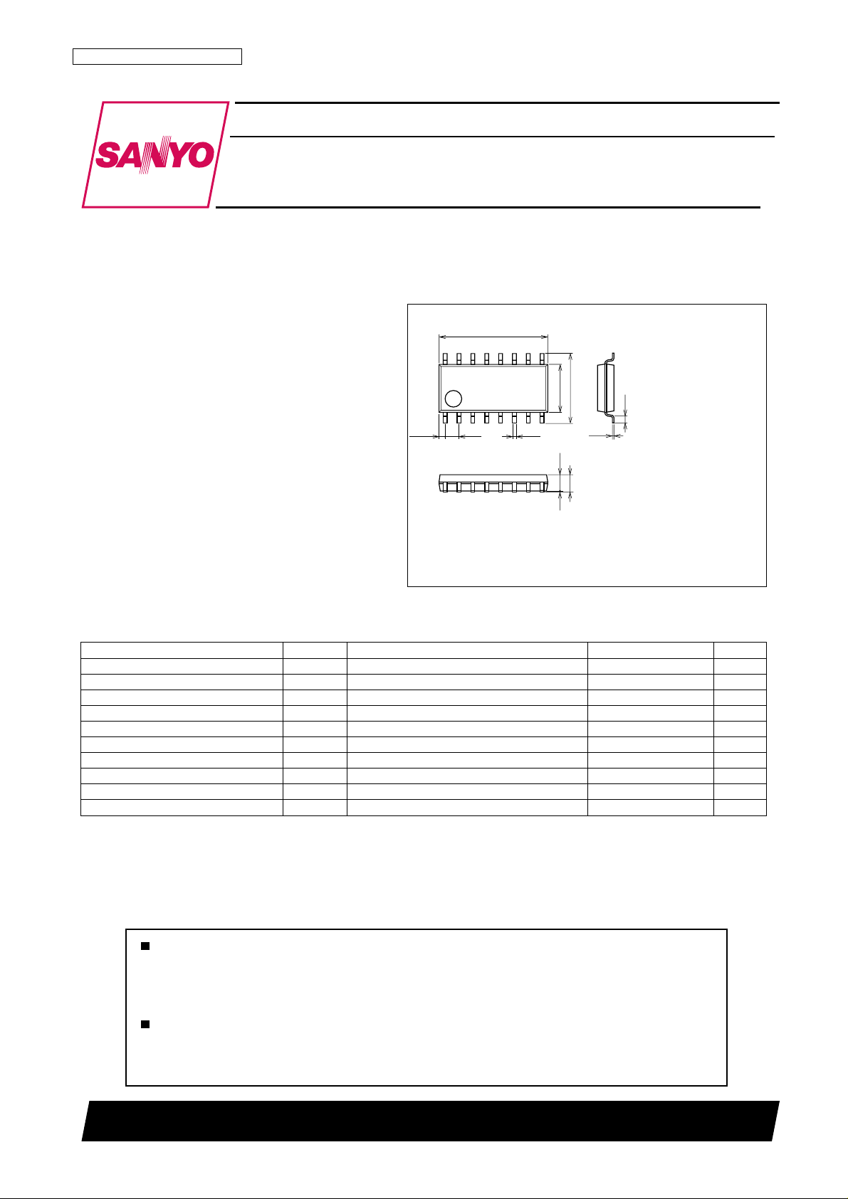
Package Dimensions
unit : mm
2198
[TND506MD]
9
4.4
8
0.35
(1.5)
0.1
(0.56)
10.0
16
1
1.27
6.4
0.63
0.15
1 : LOUT 9 : No Contact
2 : GND 10 : No Contact
3 : VL 11 : VDD
1.7max
4 : No Contact 12 : HIN
5 : No Contact 13 : SD
6 : HFG 14 : LIN
7 : VH 15 : No Contact
8 : HOUT 16 : No Contact
SANYO : MFP16(225mil)
Specifications
Absolute Maximum Ratings at T a=25°C (All voltage parameters are absolute voltage referenced to GND)
Parameter Symbol Conditions Ratings Unit
High Side Floating Supply Voltage
High Side Floating Supply Offset Voltage V
High Side Output Voltage V
Low Side Supply Voltage V
Low Side Output Voltage V
Logic Supply VoltageV
Logic Input Voltage(HIN, LIN, SD) V
Allowable Power Dissipation P
Junction T emperature Tj --55 to +150 °C
Storage T emperature T stg --55 to +150 °C
DD
V
H
HFG
HOUT
L
LOUT
IN
D
--0.3 to 625 V
VH--25 to VH+0.3 V
V
--0.3 to VH+0.3 V
HFG
Mounted on a ceramic board 0.9 W
--0.3 to 25 V
--0.3 to VL+0.3 V
--0.3 to 25 V
--0.3 to VDD+0.3 V
Any and all SANYO products described or contained herein do not have specifications that can handle
applications that require extremely high levels of reliability, such as life-support systems, aircraft's
control systems, or other applications whose failure can be reasonably expected to result in serious
physical and/or material damage. Consult with your SANYO representative nearest you before using
any SANYO products described or contained herein in such applications.
SANYO assumes no responsibility for equipment failures that result from using products at values that
exceed, even momentarily, rated values (such as maximum ratings, operating condition ranges, or other
parameters) listed in products specifications of any and all SANYO products described or contained
herein.
SANYO Electric Co.,Ltd. Semiconductor Company
TOKYO OFFICE Tokyo Bldg., 1-10, 1 Chome, Ueno, Taito-ku, TOKYO, 110-8534 JAPAN
60502 TS IM TA-100070
No.7263-1/9
Page 2
TND506MD
Recommended Operating Conditions at T a=25°C
Parameter Symbol Conditions Ratings Unit
High Side Floating Supply Voltage
High Side Floating Supply Offset Voltage V
High Side Output Voltage V
Low Side Supply Voltage V
Low Side Output Voltage V
Logic Supply Voltage V
Logic Input Voltage(HIN, LIN, SD) V
Ambient T emperature T opr --40 to +125 °C
V
H
HFG
HOUT
L
LOUT
DD
IN
V
HFG
+10 to V
V
HFG
+20 V
HFG
0 to 600 V
to V
H
10 to +20 V
0 to V
L
+5 to +20 V
0 to V
DD
V
V
V
AC Characteristics at Ta=25°C (VDD=VL=V
Parameter Symbol Conditions
Turn-ON Delay Time t
Turn-OFF Delay Time t
Shutdown Delay Time tsd V
Turn-ON Rise Time t
Turn-OFF Fall Time t
Delay Matching, HS and LS Turn-ON Mt
Delay Matching, HS and LS Turn-OFF Mt
on
off
V
V
r
f
on Hton
off Htoff
DC Characteristics at Ta=25°C, (VDD=VL=V
Parameter Symbol Conditions
VDD=5V 3.2 V
Logic “1” Input Voltage V
Logic “0” Input Voltage V
High-level Output Voltage, VBIAS-VO V
Low-level Output Voltage, VO V
Offset Supply Leakage Current I
Quiescent VH Supply Current I
Quiescent VL Supply Current I
Quiescent VDD Supply Current I
Logic “1” Input Bias Current IIN+VIN=V
Logic “0” Input Bias Current IIN-- VIN=0V 1 µA
VH Supply Undervoltage
Positive Going Threshold
VH Supply Undervoltage
Negative Going Threshold
VL Supply Undervoltage
Positive Going Threshold
VL Supply Undervoltage
Negative Going Threshold
Output High Short Circuit Pulsed Current IO+V
Output Low Short Circuit Pulsed Current IO-- V
V
V
V
V
OH
OL
LK
QH
QL
QDD
HUV
HUV
LUV
LUV
VDD=10V 6.4 V
IH
VDD=15V 9.5 V
VDD=20V 12.8 V
VDD=5V 1.5 V
VDD=10V 3.7 V
IL
VDD=15V 5.8 V
VDD=20V 7.7 V
VIN=VIH, IO=0A 0.1 V
VIN=VIL, IO=0A 0.1 V
VH=V
VIN=0V or V
VIN=0V or V
VIN=0V or V
+
--
+
--
=15V, CL=1000pF)
HHFG
Ratings
min typ max
=0V 105 150 195 ns
HFG
=600V 84 120 156 ns
HFG
=600V 120 ns
HFG
-Lt
on
-Lt
off
=15V)
HHFG
min typ max
=600V 10 µA
HFG
DD
DD
DD
DD
7.6 8.9 9.9 V
6.7 8.1 9.5 V
7.6 8.9 9.9 V
6.7 8.1 9.5 V
=0V, VIN=15V, PW≤10µs 220 250 mA
OUT
=15V, VIN=0V, PW≤10µs 450 500 mA
OUT
120 ns
60 ns
15 ns
15 ns
Ratings
35 60 µA
120 200 µA
520µA
20 55 µA
Unit
Unit
No.7263-2/9
Page 3
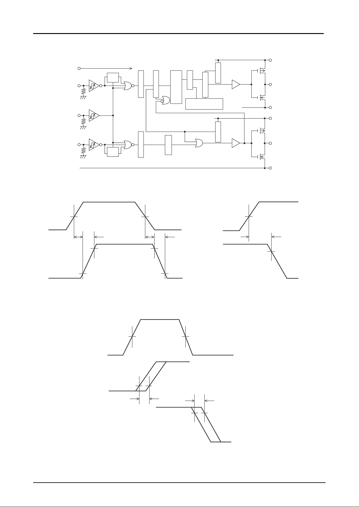
Functional Block Diagram
VDD
HIN
SD
RQ
S
Level Shift
Pulse Gain
TND506MD
Filter
Level Shift
High Voltage
Supervisory Circuit
Latch Circuit
Low Side
UV Circuit
VH
HOUT
HFG
VL
LIN
S
RQ
Level Shift
UV Circuit
Delay
LOUT
GND
Switching Time Waveform Definition Shutdown Waveform Definition
HIN
LIN
HOUT
LOUT
50% 50%
t
on
t
r
SD
t
off
90%90%
t
f
HOUT
LOUT
10%10%
50%
t
sd
90%
Delay Matching Waveform Definition
HIN
LIN
10%
50%
HOUT
90%
LOUT
M
toff
HOUT
50%
LOUT
M
ton
No.7263-3/9
Page 4

Switching Time Test Circuit
10µF 0.1µF
HIN
SD
LIN
VDD=15V
11
12
13
14
TND506MD
73
6
8
1
2
0.1µF10µF
C
L
HOUT
LOUT
C
L
10µF
VH
+
15V
-HFG
(0 to 600V)
300
250
-- ns
on
200
150
100
Turn-ON Delay Time, t
300
250
-- ns
off
200
150
100
V
HFG
VDD=VL=V
50
0
--50 0 25 75 12550 100--25
ton -- Tc
=0V
HHFG
=10V
V
L
15V
Case Temperature, Tc -- °C
t
-- Tc
off
=10V
V
L
15V
20V
20V
V
=600V
HFG
VDD=VL=V
IT03827
HHFG
300
250
-- ns
on
200
150
100
Turn-ON Delay Time, t
50
0
10 16 2014 1812
300
250
-- ns
off
200
150
100
ton -- VDD, VL, V
typ
VDD, VL, V
t
-- VDD, VL, V
off
HHFG
typ
HHFG
-- V
HHFG
V
V
HFG
HFG
=0V
IT03828
=600V
Turn-OFF Delay Time, t
50
0
0
--50 0 25 75 12550 100--25
Case Temperature, Tc -- °C
IT03829
Turn-OFF Delay Time, t
50
0
10 16 2014 1812
VDD, VL, V
HHFG
-- V
IT03830
No.7263-4/9
Page 5

-- ns
300
250
200
150
100
tsd -- Tc
=10V
V
L
15V
20V
V
=600V
HFG
VDD=VL=V
TND506MD
HHFG
-- ns
300
250
200
150
100
tsd -- VDD, VL, V
typ
HHFG
V
HFG
=600V
Shutdown Delay Time, tsd
50
0
--50 0 25 75 12550 100--25
200
150
-- ns
r
100
50
Turn-ON Rise Time, t
0
--50 0 25 75 12550 100--25
120
100
-- ns
f
80
60
40
CL=1000pF
VDD=VL=V
CL=1000pF
VDD=VL=V
Case Temperature, Tc -- °C
tr -- Tc
HHFG
=10V
L
V
15V
20V
Case Temperature, Tc -- °C
tf -- Tc
HHFG
=10V
L
V
15V
20V
IT03831
IT03833
Shutdown Delay Time, tsd
50
0
10 16 2014 1812
200
150
-- ns
r
100
50
Turn-ON Rise Time, t
0
10 14 2016 1812
120
100
-- ns
f
80
60
40
VDD, VL, V
HHFG
tr -- VDD, VL, V
typ
VDD, VL, V
HHFG
tf -- VDD, VL, V
typ
-- V
HHFG
-- V
HHFG
IT03832
CL=1000pF
IT03834
CL=1000pF
Turn-OFF Fall Time, t
-- V
IH
Logic "1" Input Voltage, V
20
0
--50 0 25 75 12550 100--25
14
12
10
8
6
4
2
0
--50 0 25 75 12550 100--25
Case Temperature, Tc -- °C
VIH -- Tc
min
Case Temperature, Tc -- °C
IT03835
VDD=15V
IT03837
Turn-OFF Fall Time, t
20
0
10 16 2014 1812
14
12
-- V
10
IH
8
6
4
Logic "1" Input Voltage, V
2
0
5.0 7.5 15.0 20.012.5 17.510.0
VDD, VL, V
HHFG
VIH -- V
DD
min
Logic Supply Voltage, V
-- V
DD
-- V
IT03836
IT03838
No.7263-5/9
Page 6

-- V
IL
TND506MD
14
12
VIL -- Tc
VDD=15V
14
12
-- V
10
IL
10
VIL -- V
DD
8
6
max
8
6
max
4
Logic "0" Input Voltage, V
2
0
--50 0 25 75 12550 100--25 5.0 7.5 10.0 12.5 15.0 17.5 20.0
VIN=V
IO=0A
VIN=V
IO=0A
IT03839
IH
IT03841
IL
-- mV
), V
-- V
High-level Output Voltage
(V
-- mV
), V
200
175
150
125
OH
100
O
75
BIAS
50
25
0
--50 0 25 75 12550 100--25
200
175
OL
150
O
125
100
Case Temperature, Tc -- °C
VOH -- Tc
max
Case Temperature, Tc -- °C
VOL -- Tc
max
Logic "0" Input Voltage, V
-- mV
OH
), V
O
-- V
BIAS
High-level Output Voltage
(V
-- mV
OL
), V
O
4
2
0
200
175
150
125
100
75
50
25
0
10 14 2016 1812
200
175
150
125
100
Logic Supply Voltage, V
VOH -- V
L, VHHFG
max
VL, V
VOL -- V
-- V
HHFG
L, VHHFG
max
DD
-- V
VIN=V
IO=0A
VIN=V
IO=0A
IT03840
IH
IT03842
IL
75
50
25
Low-level Output Voltage(V
0
--50 0 25 75 12550 100--25
Case Temperature, Tc -- °C
50
-- µA
40
LK
30
20
10
Offset Supply Leakage Current, I
0
--50 0 25 75 12550 100--25
Case Temperature, Tc -- °C
ILK -- Tc
max
VH=V
HFG
IT03843
=600V
IT03845
75
50
25
Low-level Output Voltage(V
0
10 16 2014 1812
VL, V
50
-- µA
40
LK
30
20
10
Offset Supply Leakage Current, I
0
0 100 400 600300 500200
ILK -- V
High Side Floating Supply Voltage, V
HHFG
max
-- V
H
H
VH=V
-- V
IT03844
HFG
IT03846
No.7263-6/9
Page 7

-- µA
QH
100
TND506MD
IQH -- Tc
VIN=V
V
80
HHFG
IH
=15V
or V
IL
100
-- µA
80
QH
60
max
60
IQH -- V
max
HHFG
VIN=V
IH
or V
IL
40
Supply Current, I
H
20
Quiescent V
0
--50 0 25 75 12550 100--25 10 14 2016 1812
Case Temperature, Tc -- °C
300
250
-- µA
QL
200
150
Supply Current, I
100
L
50
typ
IQL -- Tc
max
typ
VIN=V
VL=15V
IH
IT03847
or V
IL
Quiescent V
0
--50 0 25 75 12550 100--25
IT03849
IL
30
-- µA
25
QDD
20
Case Temperature, Tc -- °C
I
-- Tc
QDD
VIN=VIH or V
VDD=15V
max
40
Supply Current, I
H
20
Quiescent V
0
300
-- µA
250
QL
200
150
Supply Current, I
100
L
50
Quiescent V
0
10 14 2016 1812
30
-- µA
25
QDD
20
VIN=V
typ
V
HHFG
-- V
IQL -- V
or V
IH
IL
max
typ
Low Side Supply Voltage, V
I
-- V
QDD
max
L
DD
-- V
L
VIN=V
IH
IT03848
IT03850
or V
IL
15
Supply Current, I
10
DD
5
Quiescent V
0
--50 0 25 75 12550 100--25
Case Temperature, Tc -- °C
80
VIN=VDD=15V
-- µA
(+)
60
IN
40
20
Logic "1" Input Bias Current, I
0
--50 0 25 75 12550 100--25
IIN(+) -- Tc
Case Temperature, Tc -- °C
typ
max
typ
IT03851
IT03853
15
Supply Current, I
10
DD
5
Quiescent V
0
10 14 2016 1812
Logic Supply Voltage, V
80
-- µA
(+)
60
IN
40
20
Logic "1" Input Bias Current, I
0
10 14 2016 1812
IIN(+) -- V
Logic Supply Voltage, V
typ
max
typ
DD
DD
DD
-- V
-- V
IT03852
VIN=15V
IT03854
No.7263-7/9
Page 8

-- µA
(–)
IN
TND506MD
5
IIN(–) -- Tc
VIN=0V
VDD=15V
4
-- µA
(–)
5
4
IN
3
3
IIN(–) -- V
DD
VIN=0V
2
V
HUV
max
IT03855
(+) -- Tc
max
typ
1
Logic "0" Input Bias Current, I
0
--50 0 25 75 12550 100--25
Case Temperature, Tc -- °C
11
10
-- µA
(+)
9
HUV
8
min
7
Supply Undervoltage Positive
H
V
Going Threshold, V
6
--50 0 25 75 12550 100--25 --50 0 25 75 12550 100--25
Case Temperature, Tc -- °C
V
(+) -- Tc
11
LUV
IT03857
Supply Undervoltage Negative
H
V
2
1
Logic "0" Input Bias Current, I
0
10 14 2016 1812
Logic Supply Voltage, V
V
HUV
-- µA
(–)
11
10
9
HUV
8
7
Going Threshold, V
6
Case Temperature, Tc -- °C
V
11
LUV
max
DD
(–) -- Tc
max
typ
min
(–) -- Tc
-- V
IT03856
IT03858
-- µA
(+)
LUV
10
9
8
max
typ
min
Supply Undervoltage Positive
7
L
Going Threshold, V
V
6
--50 0 25 75 12550 100--25 --50 0 25 75 12550 100--25
IT03859
V
=0V
OUT
VIN=15V
PW≤10µs
-- mA
(+)
O
, I
500
400
300
200
Case Temperature, Tc -- °C
IO(+) -- Tc
V
=20V
L
15V
Supply Undervoltage Negative
L
V
10V
Output High Short Circuit
Pulsed Current
100
Output High Short Circuit
10
-- µA
(–)
9
LUV
8
7
Going Threshold, V
6
500
400
-- mA
(+)
300
O
, I
200
Pulsed Current
100
max
typ
min
Case Temperature, Tc -- °C
IO(+) -- VL, V
HHFG
typ
IT03860
VIN=15V
PW≤10µs
0
--50 0 25 75 12550 100--25
Case Temperature, Tc -- °C
IT03861
0
10 12 16 201814
VL, V
HHFG
-- V
IT03862
No.7263-8/9
Page 9

1000
-- mA
(–)
O
, I
800
600
IO(--) -- Tc
V
=20V
L
15V
V
=0V
OUT
VIN=15V
PW≤10µs
TND506MD
-- mA
(–)
, I
O
1000
800
600
IO(–) -- VL, V
typ
HHFG
VIN=15V
PW≤10µs
400
10V
Output Low Short Circuit
Pulsed Current
200
0
--50 0 25 75 12550 100--25
Case Temperature, Tc -- °C
P
-- Ta
1.0
0.9
-- W
0.8
D
0.7
0.6
0.5
0.4
0.3
0.2
0.1
Allowable Power Dissipation, P
0
--40 400 80 120 160
D
Ambient Temperature, Ta -- °C
IT03863
IT04074
400
Output Low Short Circuit
Pulsed Current
200
0
10 12 16 201814
VL, V
HHFG
-- V
IT03864
Specifications of any and all SANYO products described or contained herein stipulate the performance,
characteristics, and functions of the described products in the independent state, and are not guarantees
of the performance, characteristics, and functions of the described products as mounted in the customer's
products or equipment. To verify symptoms and states that cannot be evaluated in an independent device,
the customer should always evaluate and test devices mounted in the customer's products or equipment.
SANYO Electric Co., Ltd. strives to supply high-quality high-reliability products. However, any and all
semiconductor products fail with some probability. It is possible that these probabilistic failures could
give rise to accidents or events that could endanger human lives, that could give rise to smoke or fire,
or that could cause damage to other property. When designing equipment, adopt safety measures so
that these kinds of accidents or events cannot occur. Such measures include but are not limited to protective
circuits and error prevention circuits for safe design, redundant design, and structural design.
In the event that any or all SANYO products(including technical data,services) described or
contained herein are controlled under any of applicable local export control laws and regulations,
such products must not be exported without obtaining the export license from the authorities
concerned in accordance with the above law.
No part of this publication may be reproduced or transmitted in any form or by any means, electronic or
mechanical, including photocopying and recording, or any information storage or retrieval system,
or otherwise, without the prior written permission of SANYO Electric Co. , Ltd.
Any and all information described or contained herein are subject to change without notice due to
product/technology improvement, etc. When designing equipment, refer to the "Delivery Specification"
for the SANYO product that you intend to use.
Information (including circuit diagrams and circuit parameters) herein is for example only ; it is not
guaranteed for volume production. SANYO believes information herein is accurate and reliable, but
no guarantees are made or implied regarding its use or any infringements of intellectual property rights
or other rights of third parties.
This catalog provides information as of June, 2002. Specifications and information herein are subject
to change without notice.
No.7263-9/9
PS
 Loading...