Ordering number : ENN7085A
Preliminary
TND303S
ExPD (Excellent Power Device)
TND303S
General Purpose Driver for PDP Sustain Pulse Drive, DC / AC Motor
Drive, Switching Power Supply, DC / DC Converter Applications
Features
•
Inverter buffer .
•
Monolithic structure(High voltage CMOS process
adopted).
•
Withstand voltage of 25V is assured.
•
Wide range of operating voltage : 4.5V to 25V.
•
Peak outpout current : 2A.
•
Fast switching time(25ns typical at 1000pF load).
•
Fully compatible input to TTL/CMOS.
(VIH=not more than 2.6V, at VDD=4.5 to 25V)
Specifications
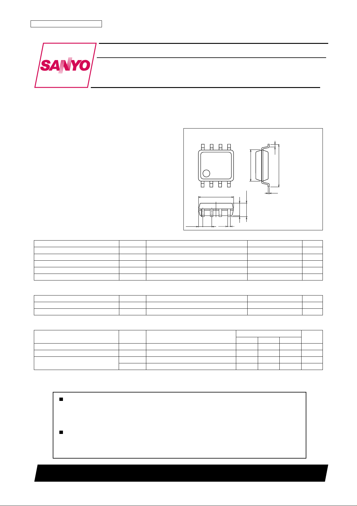
Package Dimensions
unit : mm
2199
[TND303S]
58
4.4
14
5.0
1.8max
1.5
0.595
1.27
0.43
0.1
0.3
6.0
0.2
1 : NC
2 : IN A
3 : GND
4 : IN B
5 : OUT B
6 : VDD
7 : OUT A
8 : NC
SANYO : SOP8
Absolute Maximum Ratings at T a=25°C
Parameter Symbol Conditions Ratings Unit
Supply Voltage V
Input Voltage V
Allowable Power Dissipation PD max 0.3 W
Junction T emperature Tj --55 to +150 °C
Storage T emperature T stg --55 to +150 °C
DD
IN
GND--0.3 to VDD+0.3 V
0 to 25 V
Recommended Operating Conditions at Ta=25°C
Parameter Symbol Conditions Ratings Unit
Operating Supply Voltage V
Operating T emperature T opr --40 to +125 °C
DD
4.5 to 25 V
Electrical Characteristics (AC Characteristics) at T a=25°C, VDD=18V, VIN=5V
Parameter Symbol Conditions
Turn-On Rise Time t
Turn-Off Fall Time t
Delay Time
Any and all SANYO products described or contained herein do not have specifications that can handle
applications that require extremely high levels of reliability, such as life-support systems, aircraft's
control systems, or other applications whose failure can be reasonably expected to result in serious
physical and/or material damage. Consult with your SANYO representative nearest you before using
any SANYO products described or contained herein in such applications.
SANYO assumes no responsibility for equipment failures that result from using products at values that
exceed, even momentarily, rated values (such as maximum ratings, operating condition ranges, or other
parameters) listed in products specifications of any and all SANYO products described or contained
herein.
CL=1000pF 20 35 ns
r
CL=1000pF 25 40 ns
f
tD1C
tD2C
=1000pF 30 45 ns
L
=1000pF 45 60 ns
L
Ratings
min typ max
Unit
SANYO Electric Co.,Ltd. Semiconductor Company
TOKYO OFFICE Tokyo Bldg., 1-10, 1 Chome, Ueno, Taito-ku, TOKYO, 110-8534 JAPAN
62003 TS IM TA-100712 / O0501 TS IM TA-3492
No.7085-1/4

TND303S
Electrical Characteristics (DC Characteristics) at Ta=25°C, VDD=4.5 to 25V
Parameter Symbol Conditions
Logic “1” Input Voltage V
Logic “0” Input Voltage V
Input Bias Current I
High Level Output Voltage V
Low Level Output Voltage V
VDD Supply Current Isupp
Output High Short Circuit Pulsed Current IO+VDD=18V, PW≤10µs, V
Output Low Short Circuit Pulsed Current IO-- VDD=18V, PW≤10µs, V
Output On Resistance R
IH
IL
IN
OH
OL
OUT
VIN=0 or V
IO=0 VDD--0.1 V
IO=0 0.1 V
VDD=10V, VIN=3V, (both inputs) 1.0 4.5 mA
VDD=10V, VIN=0, (both inputs) 0.2 mA
VDD=18V, Iload=10mA, V
VDD=18V, Iload=10mA, V
DD
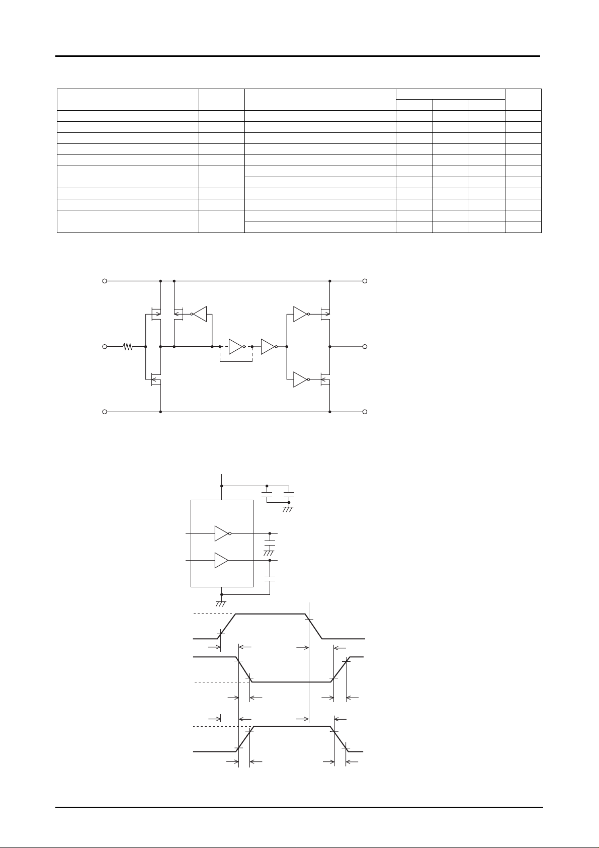
Block Diagram
V
DD
IN OUT
INVERTING
NON-INVERTING
Ratings
min typ max
2.6 V
--1 1 µ A
=0 2.0 A
OUT
=18V 2.0 A
OUT
=“H” 4 6 Ω
OUT
=“L” 3 5 Ω
OUT
Unit
0.8 V
GND
Switching Time Measuring Circuit
VDD=18V
TND303S
INPUT A
INPUT B
INPUT RISE
AND FALL
TIMES=5ns
INVERTING
OUTPUT
+5V
+0.4V
+18V
0V
10%
4.7µF
INPUT
tD1
10%
t
f
0.1µF
OUTPUT A
1000pF
OUTPUT B
1000pF
90%
tD2
10%
t
r
90%90%
NONINVERTING
OUTPUT
+18V
0V
10%
t
r
tD1
90%
90%
tD2
10%
t
f
No.7085-2/4
 Loading...