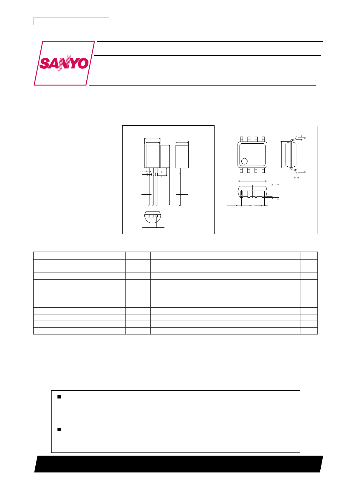
SANYO TND017SW, TND017MP Datasheet

Any and all SANYO products described or contained herein do not have specifications that can handle
applications that require extremely high levels of reliability, such as life-support systems, aircraft’s
control systems, or other applications whose failure can be reasonably expected to result in serious
physical and/or material damage. Consult with your SANYO representative nearest you before using
any SANYO products described or contained herein in such applications.
SANYO assumes no responsibility for equipment failures that result from using products at values that
exceed, even momentarily, rated values (such as maximum ratings, operating condition ranges,or other
parameters) listed in products specifications of any and all SANYO products described or contained
herein.
ExPD (Excellent Power Device)
Lowside Power Switch
Lamp, Solenoid, and Motor-Driving Applications
Ordering number:ENN6481A
TND017MP , TND017SW
SANYO Electric Co.,Ltd. Semiconductor Company
TOKYO OFFICE Tokyo Bldg., 1-10, 1 Chome, Ueno, Taito-ku, TOKYO, 110-8534 JAPAN
6.0
58
Features
· N-channel MOSFET built in.
· Overheat protection.
· Overcurrent protection.
Package Dimensions
Unit:mm
2145
(Self recovery type current
limiting function)
· Overvoltage protection.
· TND017SW incorporates two
sets of circuit.
Absolute Maximum Ratings at Ta = 25˚C
retemaraPlobmySsnoitidnoCsgnitaRtinU
egatloVecruoS-ot-niarDV
tnerruCtuptuOI
egatloVtupnIV
noitapissiDrewoPelbawollAP
egatloVylppuSgnitarepOV
erutarepmeTgnitarepOrpoT 58+ot04–
erutarepmeTnoitcnuJjT detimiLyllanretnI
erutarepmeTegarotSgtsT 051+ot55–
O
D
SD
Package Dimensions
Unit:mm
2181
[TND017MP]
5.0
0.5
0.6
6.0
0.5
23
1
1.45
1.45
SD
)CD( 5.1A
NI
Mounted on a ceramic board (1200mm2×0.8mm) 1unit
Mounted on a ceramic board (1200mm
)rpo( 04V
4.7
8.5
3.0
14.0
0.5
1 : GND
2 : OUT
3 : IN
SANYO : MP
PM710DNT 0.1W
WS710DNT
WS710DNT
[TND017SW]
14
5.0
1.5
0.595
2
×0.8mm)
1.27
0.43
0.1
0.3
4.4
0.2
1 : GND1
1.8max
2 : IN1
3 : GND2
4 : IN2
5 : OUT2
6 : OUT2
7 : OUT1
8 : OUT1
SANYO : SOP8
06V
01+ot3.0–V
7.1W
0.2W
6.0
˚C
˚C
˚C
12501TS TA-3183/42000TS (KOTO) TA-2832 No.6481–1/5

TND017MP, 017SW
Electrical Characteristics at Ta = 25˚C
retemaraPlobmySsnoitidnoC
egatloVpmalCecruoS-ot-niarDV
tnerruCFFO-tuptuO
egatloVdlohserhTtupnI
egatloVtupnIgnitarepOtiucriCnoitcetorP
ecnatsiseRNOecruoS-ot-niarDR
)NOtuptuO(tnerruCtupnII
erutarepmeTgnitceteDtaehrevO)ds(jTVNII,V5=
tnerruCgnitceteDtnerrucrevOsIVNIV5=
)kaeP(timiLtnerrucrevOI
egatloVpmalCtupnIV
pmalcVNII,0=
SD
I
)1(VNIV,0=
SSD
I
)2(VNIV,0=
SSD
VNI)ht(VSDI,V5=
VNI)rpo(
)no(VNII,V5=
SD
VNIV5=
NI
VNIV5=
TML
pmalc,INIAm1=
NI
Am1=06V
O
V05=01Aµ
SD
V21=
SD
Am1=
O
A1=
O
A1=
O
Notes : 1. Overcurrent protection circuit limits the output current to the range of overcurrent limit value.
2. During overheat protecting operation, output current is once turned off and then recovers after the input voltage falls to the reset voltage
(1.0V) or below.
nimpytxam
0.15.10.2V
401V
021051091
0.30.40.5A
5.35.45.5A
01V
sgnitaR
5Aµ
3.04.0
52.06.0Am
tinU
Ω
˚C
Block Diagram
IN
ESD
protection
0.5
– Ω
0.4
(on)
DS
0.3
0.2
0.1
Overheat
protection
Overcurrent
protection
Output current
control
RDS(on) -- Ta
=4V
V
IN
6V
OUT(D)
Overvoltage
protection
Gate
shutdown
Latch
GND(S)
RDS(on) -- V
IO=1A IO=1A
5V
– Ω
(on)
DS
0.6
0.5
0.4
0.3
0.2
0.1
IN
Ta=85
25°C
--40°C
°C
0
--50 --25 0 25 50 75 100
Drain-to-Source ON Resistance, R
0.6
Ambient Temperature, Ta – ˚C
I
-- Ta
IN
VIN=5V
0.5
0.4
–mA
IN
0.3
0.2
Input Current, I
0.1
0
--50 --25 0 25 50 75 100
Ambient Temperature, Ta – ˚C
0
2345678910
IT02011 IT02012
Drain-to-Source ON Resistance, R
1.0
0.9
0.8
0.7
–mA
0.6
IN
0.5
0.4
0.3
Input Current, I
0.2
0.1
0
012345678910
IT02013 IT02014
Input Voltage, VIN–V
I
-- V
IN
IN
Protection operation
Normal operation
Input Voltage, VIN–V
Ta=25°C
No.6481–2/5
 Loading...