

Page 1
Global LCD Panel Exchange Center
www.panelook.com
One step solution for LCD / PDP / OLED panel application: Datasheet, inventory and accessory!
www.panelook.com
Page 2
Global LCD Panel Exchange Center
NOTICES
1. The contents stated in this document and the product may be subject to
change without prior notice.
When you kindly study to use this product, please ask our distributor or us
for the latest information.
2. This product is developed and produced for usage onto normal electronic
products (office automation equipments, communication peripherals, electric
appliance products, game machines, etc.) and is not suitable for applications
which need extremely high reliability or extreme safety (aero- or space-use
machines, control equipments for nuclear power, life keeping equipments,
etc.).
3. This document shall not grant or guarantee any right to adapt intellectual
property or any other patents of third party.
4. Please use this product correctly according to operating conditions and
precautions for use stated in this document.
Please install safety proof in your designing to avoid human accident, fire
accident and social damage, which may be resulted from malfunction of this
product.
www.panelook.com
5. This product is not designed to withstand against radiant rays.
6. It is strictly prohibited to copy or publish a part or whole of this document
without our prior written approval.
REVISION HISTORY
DATE REVISION
NO.
Jul.8,04 Ver. 1 - Initial Release
Oct.22,04 Ver. 2
Mar.29,04 Ver. 3
SANYO EPSON IMAGING DEVICES
CORPORATION
PAGE DESCRIPTIONS
Weight:TBD->690 TYP. 2
Power Supply current:TBD->250
3 Color of CIE coordinate Rx,y;Gx,y;Bx,y:TBD->(xxx)
4
8 DCLK f
2,3,4,9,11 (xxx)->xxx
8
9 Eliminate the Duty,tSI,tHP,tSD,tHD: (xxx)->xxx
11
BACKLIGHT CHARACTERISTIC:TBD->xxx
:(41)->(50.8),DE fH(40)->(48.1),DE fV:(62)->(75)
CLK
Add the INTERFACE (LVDS) SIGNAL TIMING PARAMETERS
POWER ON/OFF SEQUENCE REQUIREMENT
Add the VCM
Change the character: VIH -> VTH
Change the character: V
TM121SVA01
IL -> VTL
Ver. 3
Page
1/16
One step solution for LCD / PDP / OLED panel application: Datasheet, inventory and accessory!
www.panelook.com
Page 3
Global LCD Panel Exchange Center
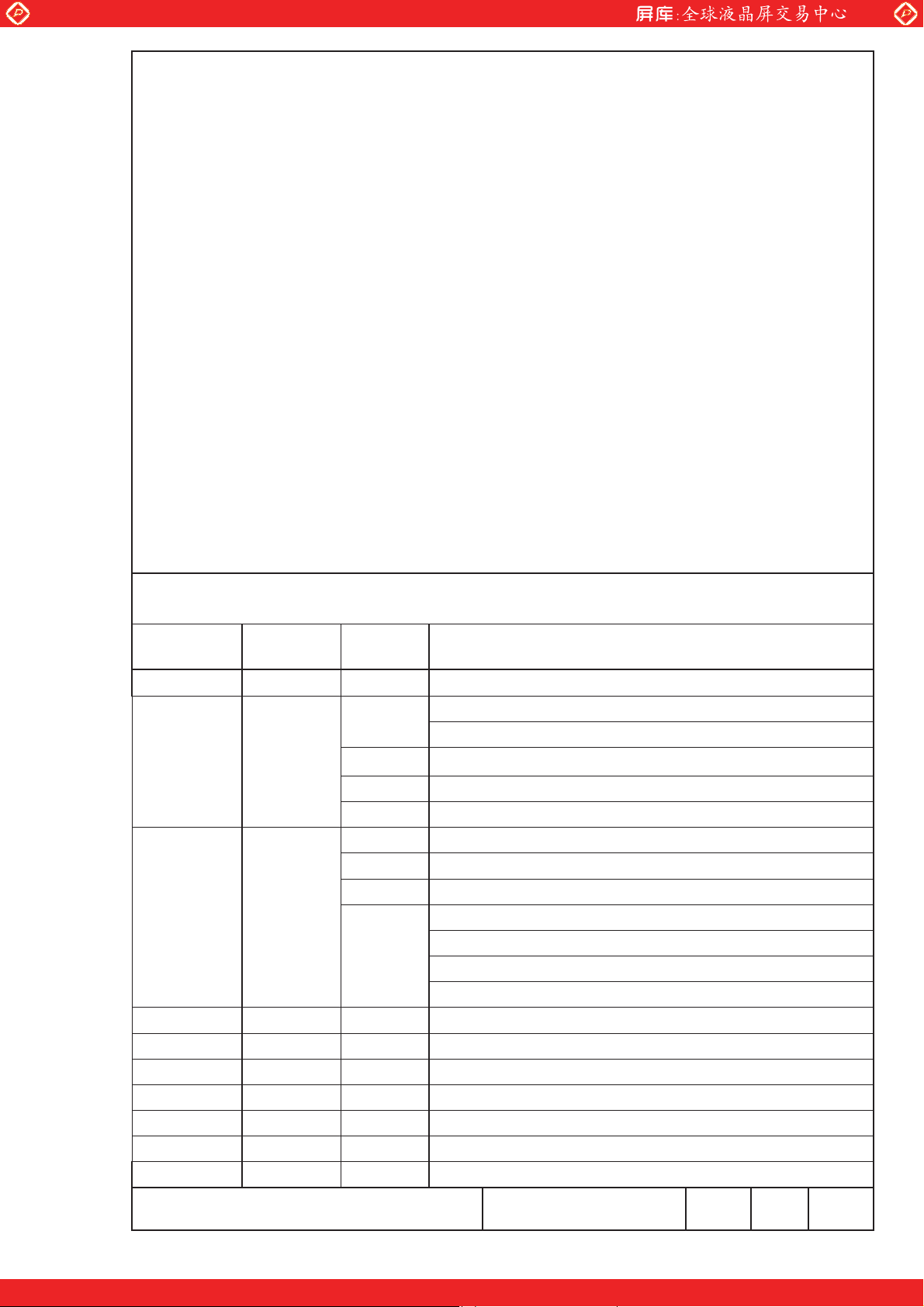
MECHANICAL CHARACTERISTICS
ITEM SPECIFICATION UNIT
Module size 280.0(W) x 218.0(H) x 11.5 Typ.(t) mm
Resolution
Sub pixel pitch 0.1025(W) x 0.3075(H) mm
Pixel pitch 0.3075(W) x 0.3075(H) mm
Active viewing area 246.0(W) x 184.5(H) mm
Bezel opening area 249.0(W) x 187.5(H) mm
Weight 690 TYP. g
ELECTRICAL ABSOLUTE MAXIMUM RATINGS
ITEM SYMBOL MIN MAX UNIT NOTE
Power supply voltage VDD-VSS 0 4.0 V
Input voltage VI Vss-0.3 VDD+0.3 V
Lamp current IL - 8 mA
Lamp supply voltage
www.panelook.com
Ta=25 degC
800 x R㨯G㨯B(W) x 600(H)
Ta=25 degC
VHV - 2000 Vrms
V
LGND - 100 Vrms
pixel
ENVIRONMENTAL ABSOLUTE MAXIMUM RATINGS
ITEM SYMBOL CONDITIONS MIN MAX UNIT NOTE
TST Storage -20 60 Ambient
temperature
Humidity - Ta=40 degC max. - 85 %RH No condensation
Vibration - Storage - 1.5 G Note 3
Shock - Storage - 50 G XYZ 11ms/direction
OP Operation 0 50
T
degC Note 1
Note 2
[Note 1] Care should be taken so that the LCD module may not be subjected to the
temperature beyond this specification.
[Note 2] Ta>40 degC : Absolute humidity shall be less than that of 85%RH/40 degC.
[Note 3] 10-200Hz, 30min/cycle, X/Y/Z each one cycle and except for resonant frequency.
Ta=25 degC
ELECTRICAL CHARACTERISTICS
V
ITEM SYMBOL CONDITIONS MIN TYP MAX UNIT NOTE
Power supply voltage VDD-VSS 3.0 3.3 3.6 V
LVDS input
Threshold voltage
Common mode
voltage of LVDS input
LVDS input
Termination resistor
Power Supply current IDD Note 1 - 250 - mA
VTH High level - - +100
V
TL Low level -100 - -
CM 1.125 1.25 1.375 V
V
T - 100 - ohms Internal
R
DD=3.3V, fCLK=40MHz ,fH=38kHz, fV=60Hz, Ta=25 degC
mV V
CM=1.25V
[Note 1] Under the following display image :
Typical Value: Display pattern is 64 gray scale bar.
[Note 2] V
SANYO EPSON IMAGING DEVICES
CM : Common mode voltage of LVDS input
CORPORATION
TM121SVA0 1 Ver. 3
One step solution for LCD / PDP / OLED panel application: Datasheet, inventory and accessory!
Page
2/16
www.panelook.com
Page 4
Ǿ
Ǭ
Ǿ
Ǿ
ǰ
ǰ
ǰ
Ǿ
ǰ
Ǿ
Ǿ
r
㱢
㱔
㱔
㱔
㱔
㱔
㱢
㱔
㱐
㱐
Global LCD Panel Exchange Center
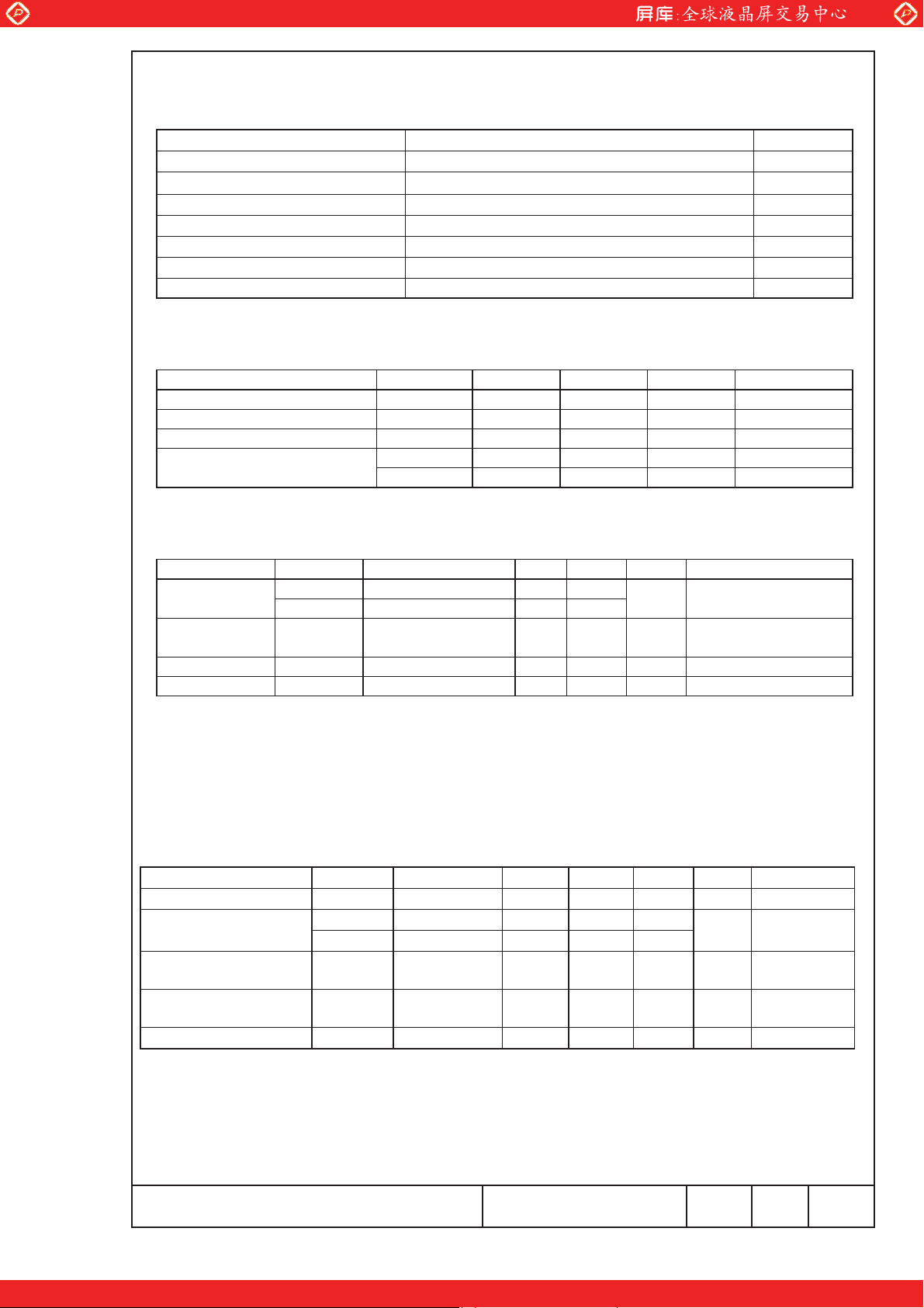
OPTICAL CHARACTERISTICS
ITEM
Brightness B
Brightness uniformity
Contrast ratio CR
Viewing angle range
Rise tr - 30 - Response
time
Color of
CIE
coordinate
Fall tf
Red
Green
Blue
White
www.panelook.com
Ta=25 degC, VDD=3.3V, fCLK=40MHz, fH=38kHz, fV=60Hz
SYMBOL
B
CONDITIONS MIN TYP
=0 deg.
=0 deg.
=0 deg.
= 0 deg.
CR>10
=0 deg.
= 90 deg.
=180 deg.
=270 deg.
- 340 -
- - 1.45 -
- 300 - -
- 40 -
- 50 -
- 20 -
- 50 -
- 20 x - 0.60 y - 0.35 x - 0.32 y - 0.56 x - 0.15 -
=0 deg.
y - 0.13 x 0.31 0.34 0.37
y
0.32 0.35 0.38
MAX
UNIT NOTE
cd/m
deg.
ms.
Note
2
5,7,8
Note
6,7,8
Note
2,4,8
Note 1,2,
4,8
Note
3,4,8
- Note 4,8
=180deg.
=270deg.
[Note 1] and [Note 3] Response time
=0deg.
=90deg.
B
Black Black
100%
90%
10%
0%
t
[Note 2] Contrast ratio "CR" is defined as :
Brightness at White
CR =
Brightness at Black
[Note 4] This shall be measured at center (point No.3 shown in Note 7).
[Note 5] The brightness shall be the average of five points.
[Note 6] The brightness uniformity "
B" is defined as :
Maximum brightness of five points
B =
Minimum brightness of five points
White DATA
tf
SANYO EPSON IMAGING DEVICES
CORPORATION
One step solution for LCD / PDP / OLED panel application: Datasheet, inventory and accessory!
TM121SVA01
Ver. 3
Page
3/16
www.panelook.com
Page 5
Global LCD Panel Exchange Center
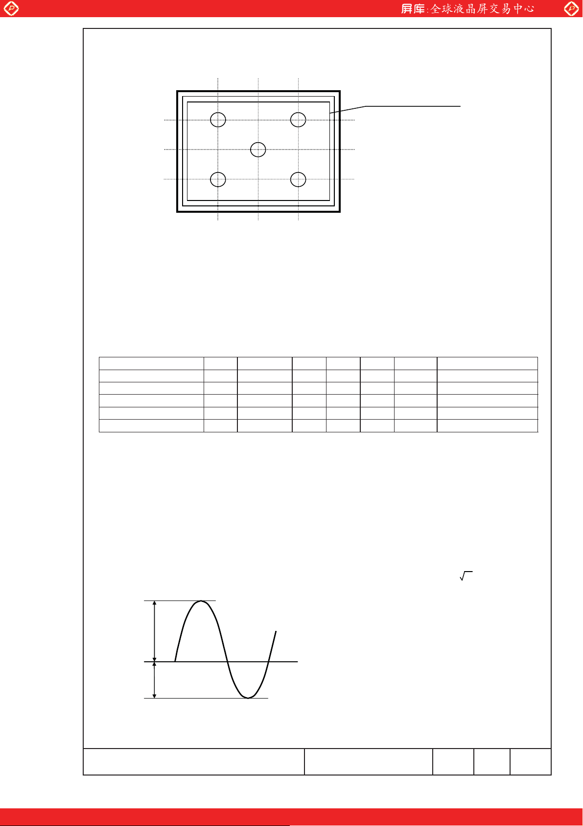
[Note 7] Measurement points
1/6Vp
www.panelook.com
5/6Hp1/2Hp1/6Hp
Active area
1 2
1/2Vp
5/6Vp
4
3
5
Vp: Total Number of Vertical pixel
Hp: Total Number of horizontal pixel
[Note 8] Measurement condition
(1) Measurement equipment: BM-5A (TOPCON Corp.), Field=2 degree
(2) Ambient temperature Ta: 25 +/- 2 degC
(3) LCD: All pixels are WHITE, V
DD=3.3V, fCLK=40MHz, fH=38kHz, fV=60Hz
(4) Measure after 30 minutes of CFL warm up.
(5) I
L=6.0mArms with the CFL inverter CXA-P1212-VJL (TDK).
BACKLIGHT CHARACTERISTICS
ITEM SYM. CONDITIOS MIN TYP MAX UNIT NOTE
Lamp voltage VL - 510 - Vrms at IL=6.0mArms
Lamp current IL 3 - 8 mArms
Operating frequency fL 40 - 65 kHz
Start up voltage VS - - 1300 Vrms at Ta=0 degC
Lamp life
tOL
Ta=25 degC
Recommended value
Recommended value
50000
- - Hours at IL=6.0 mArms
[Note 1] Backlight driving conditions (operating frequency fL especially) may interfere
with horizontal frequency f
Therefore the operating frequency f
horizontal frequency f
H, causing the beat or flicker on the display.
L shall be adjusted in relation to
H to avoid interference.
[Note 2] The inverter open voltage should be larger than start up voltage, otherwise backlight
may blinking for a moment after turns on or not be turned on. And this voltage
should be applied to lamp for more than 1 second to start up, otherwise backlight
may not be turned on.
[Note 3] If driving current waveform is asymmetrical, mercury deviation inside of CFL will
incline to one side and consequently abnormal lighting may occur.
To prevent such unfavorable lighting, driving current waveform is asked to have
unbalance rate of less than 10% and wave-height rate of less than 2 +/- 10%.
And this driving waveform shall be confirmed in your system.
Unbalance rate = | Ip - I-p | / IL x 100 (%)
Ip
I-p
Current waveform
Wave-height rate = I
I
p : High peak value
-p : Low peak value
I
I
L : Effective value
p (or I-p) / IL
[Note 4] The inverter of ground reference type should be used. The inverter of ground floating
type should not be used.
SANYO EPSON IMAGING DEVICES
CORPORATION
TM121SVA0 1 Ve r.3
One step solution for LCD / PDP / OLED panel application: Datasheet, inventory and accessory!
Page
4/16
www.panelook.com
Page 6
r
Global LCD Panel Exchange Center
www.panelook.com
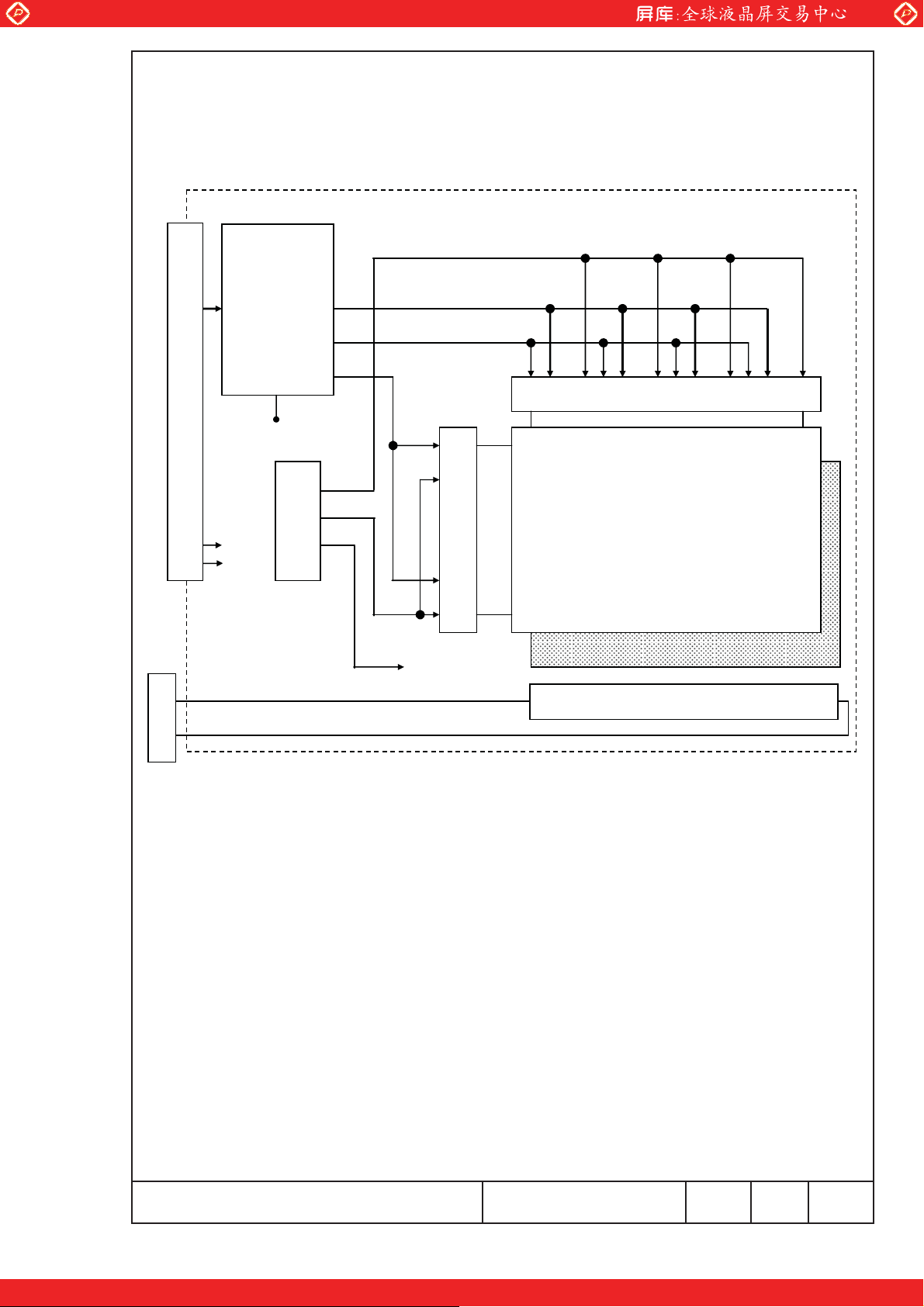
BLOCK DIAGRAM
ASIC
TFT
Timing
Generator
CN1
DE
VDD
VSS
DC/DC
(LVDS-Receiver)
Converter
DATA
Gate Drive
600
Source Driver
800(RGB)
TFT Panel
FLCN1,2
Back Light
Vcom
2CFL
SANYO EPSON IMAGING DEVICES
One step solution for LCD / PDP / OLED panel application: Datasheet, inventory and accessory!
CORPORATION
TM121SVA01
Ver. 3
Page
5/16
www.panelook.com
Page 7

Global LCD Panel Exchange Center
INTERFACE PIN CONNECTIONS
LCM : CN1
PIN NO. SYMBOL FUNCTION
1 VDD Power Supply ( 3.3V normal)
2 VDD Power Supply ( 3.3V normal)
3 VSS Ground
4 VSS Ground
5 Rin0- Receiver Signal(-)
6 Rin0+ Receiver Signal(+)
7 VSS Ground
8 Rin1- Receiver Signal(-)
9 Rin1+ Receiver Signal(+)
10 VSS Ground
11 Rin2- Receiver Signal(-)
12 Rin2+ Receiver Signal(+)
13 VSS Ground
14 RCLK- Clock Signal(-)
15 RCLK+ Clock Signal(+)
16 VSS Ground
17 NC No Connection(Should be open during operation)
18 NC No Connection(Should be open during operation)
19 VSS Ground
20 NC No Connection(Should be open during operation)
www.panelook.com
CN1 : FI-SEB20P-HF10 (JAE)
Suitable mating connector: FI-S20S/FI-SE20M/FI-SE20MR(JAE)
[Note 1] Internal termination resistors of LVDS input lines are 100 ohms.
[Note 2] Valid synchronous signals are DCLK and DE. HSYNC and VSYNC are not used
Back Light : FLCN1,2
PIN NO. SYMBOL FUNCTION
1 H.V High voltage for CFL
2 N.C. No connection
3 LGND Low voltage for CFL
FLCN1,2 : BHR-03VS-1 (JST)
Suitable mating connector: SM02(8.0)B-BHS-1 (JST)
SANYO EPSON IMAGING DEVICES
CORPORATION
TM121SVA0 1 Ve r.3
One step solution for LCD / PDP / OLED panel application: Datasheet, inventory and accessory!
Page
6/16
www.panelook.com
Page 8

(
)
(
)
(
)
Global LCD Panel Exchange Center
INTERFACE (LVDS) DATA ASSIGNMENT
Rin0 +/-
Rin1 +/-
Rin2 +/-
RCLK +/-
Rxout 6
GO(LSB)
Rxout13
Rxout20 DERxout19
www.panelook.com
Rxout 5
R5
MSB
Rxout12
VSYNC
Rxout 4
R4
Rxout11
Rxout18
HSYNC
Rxout 3
R3
Rxout10
Rxout17
B5
MSB
Rxout 2
R2
Rxout 9
Rxout16
B4
Rxout 1
R1
Rxout 8
Rxout15 B3Rxout14
Rxout 0
R0
LSB
Rxout 7
B2
INTERFACE SIGNALS
SYMBOL FUNCTION
DCLK Data Clock
HSYNC Horizontal Sync - This signal initiates a new line (negative).
VSYNC Vertical Sync - This signal initiates a new frame (negative).
DE Data Enable (positive)
R0 Red Data (LSB)
R1 Red Data
R2 Red Data
R3 Red Data
R4 Red Data
R5 Red Data (MSB)
G0 Green Data (LSB)
G1 Green Data
G2 Green Data
G3 Green Data
G4 Green Data
G5 Green Data (MSB)
B0 Blue Data (LSB)
B1 Blue Data
B2 Blue Data
B3 Blue Data
B4 Blue Data
B5 Blue Data (MSB)
[Note 1] The valid synchronous signals are DCLK and DE. HSYNC and VSYNC are invalid.
[Note 2] INTERFACE SIGNALS are loaded from LVDS-transmitter to TFT Timing generator
with LVDS sequence. (See BLOCK DIAGRAM.)
SANYO EPSON IMAGING DEVICES
CORPORATION
One step solution for LCD / PDP / OLED panel application: Datasheet, inventory and accessory!
TM121SV-A01 Ver.3
Page
7/16
www.panelook.com
Page 9

㩷
㩷
p
Global LCD Panel Exchange Center
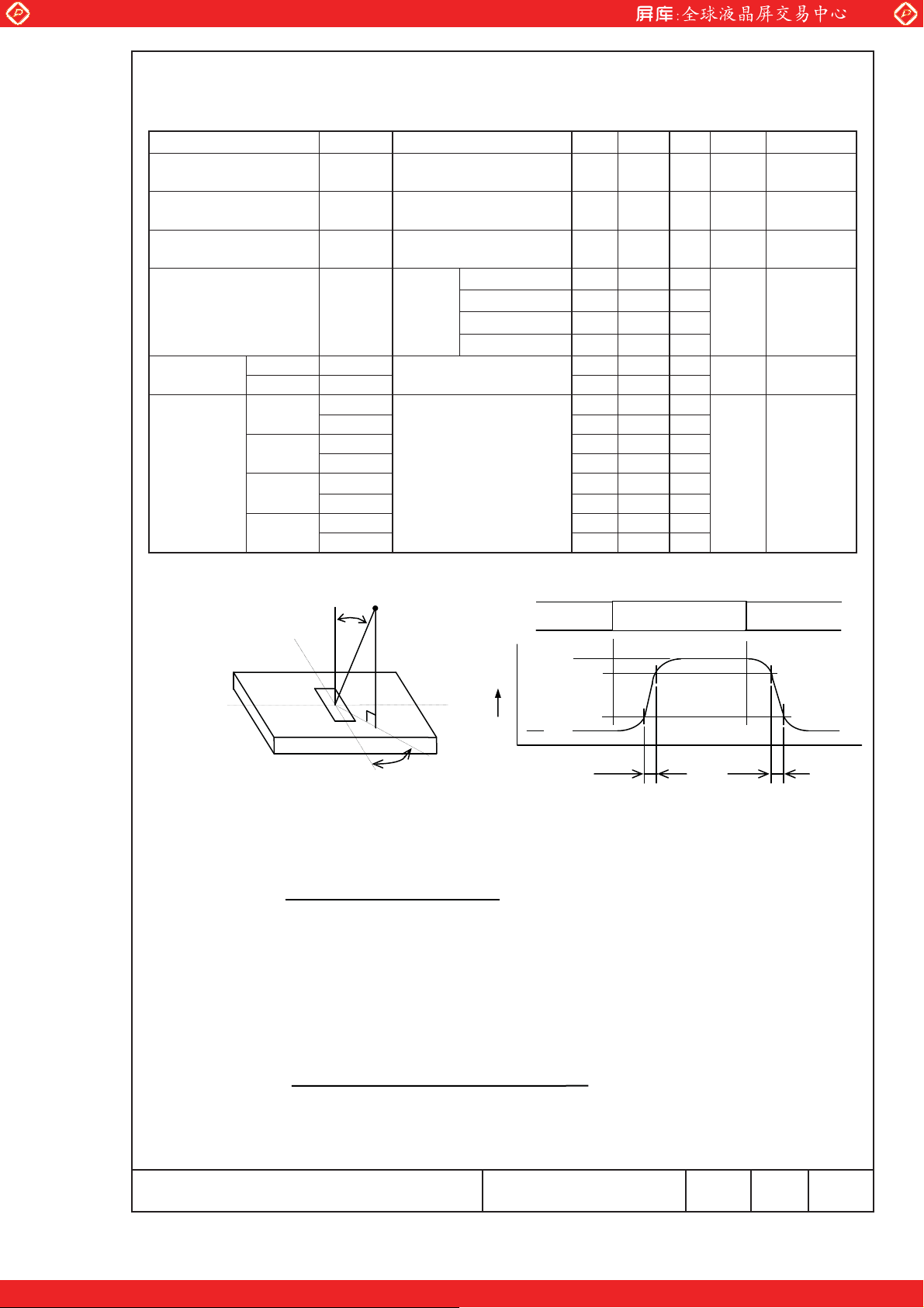
INTERFACE (LVDS) SIGNAL TIMING PARAMETERS
LVDS INPUT TIMING Ta=25 degC, VDD=3.3V, fCLK=40MHz
PARAMETER SYMBOL
Input Data Position 0 tRIP1 tCLK=25.0ns -0.9 0.0 0.9 ns
Input Data Position 1 tRIP0 tCLK=25.0ns tCLK/7-0.9 tCLK/7 tCLK /7+0.9 ns
Input Data Position 2 tRIP6 tCLK=25.0ns 2tCLK/7-0.9 2tCLK/7 2tCLK /7+0.9 ns
Input Data Position 3 tRIP5 tCLK=25.0ns 3tCLK/7-0.9 3tCLK/7 3tCLK /7+0.9 ns
Input Data Position 4 tRIP4 tCLK=25.0ns 4tCLK/7-0.9 4tCLK/7 4tCLK /7+0.9 ns
Input Data Position 5 tRIP3 tCLK=25.0ns 5tCLK/7-0.9 5tCLK/7 5tCLK /7+0.9 ns
Input Data Position 6 tRIP2 tCLK=25.0ns 6tCLK/7-0.9 6tCLK/7 6tCLK /7+0.9 ns
㩷
tRIP2
tRIP3
tRIP4
tRIP5
tRIP6
tRIP0
tRIP1
www.panelook.com
CONDITION MIN TYP MAX UNIT
Rin x +/-
LVDS In
ut Data
RX1
RX0RX2 RX6 RX5
RX4 RX3 RX2 RX1
RX0
RCLK +/-
LVDS Input Clock
Figure 1 LVDS data-input-timing waveform diagram
tCLK
JITTER TOLERANCE Ta=25 degC, VDD=3.3V, fCLK=40MHz
PARAMETER SYMBOL MIN TYP MAX UNIT
Simple cycle jitter tcj1 - - 300 ps
Clock-period change rate tcj2 - - 25 ps/cycle
㩷 㩷
*This is the value when tRIP0-6 is the typical value written in the LVDS INPUT TIMING.
The simple cycle jitter is ordinary cycle jitter.
Assuming that the period of a given clock cycle
n is represented by tCLK , for example , the
period of cycle n +1 may be tolerated up to
tCLK ±300[ps]. However , if period fluctuations
continue , the limit to that change rate , rather
than this tolerable range , constitutes the
”clock-period change rate.”
In Figure 2, the lowest clock period during this
interval is 24.9 ns, and the highest clock period
is 25.3 ns. Therefore, the clock-period change
rate during this interval is calculated from the
equation shown below.
25.3-24.9=0.4[ns]
0.4 / 5(cycles)=0.08[ns]
Because a period fluctuation of 80 ps per cycle exists here, the rated ”clock-period change
rate” in the above table is not achieved.
25.4
25.3
25.2
25.1
period (ns)
25.0
24.9
24.8
0 50 100 150
Figure 2 Example of impermissible cycle jitter
cycle
SANYO EPSON IMAGING DEVICES
CORPORATION
One step solution for LCD / PDP / OLED panel application: Datasheet, inventory and accessory!
TM121SVA01
Ver. 3
Page
8/16
www.panelook.com
Page 10

Global LCD Panel Exchange Center
INTERFACE SIGNAL TIMING PARAMETERS (DE_MODE)
PARAMETER SYMBOL MIN TYP MAX UNIT NOTE
DCLK Frequency fCLK 38 40 50.8 MHz tCLK=1/fCLK
Horiz. Period tHP 950 1056 1100 tCLK
Horiz. DE tHDE 800 800 800 tCLK
DE
[Note 1] These signal timing parameters are specified at the digital inputs of LVDS
[Note 2] The values in this table only show the normal operating conditions of internal logic
Horiz. Freq. fH 35 38 48.1 KHz fH=1/tHP
Vert. Period tVP 609 628 800 tHP fV=60Hz typical
Vert. DE nVDE 600 600 600 n
Vert. Freq. f
transmitter. With respect to setup time and hold time for DE and DATA signals,
please refer to input signal specification of LVDS transmitter.
Recommended LVDS transmitter : SN75LVDS84 (TI)
circuit, and it does not assure the conditions for appearance and display quality.
The conditions for appearance and display quality are shown in the inspection
standard separately.
www.panelook.com
V 57 60 75 Hz fV=1/tVP
INTERFACE SIGNAL TIMING DIAGRAM ( DE_MODE )
DE
DE
SANYO EPSON IMAGING DEVICES
Shrink
CORPORATION
tHDE
tHP
tVP
-----
TM121SV-A01 Ver.3
-
Page
9/16
One step solution for LCD / PDP / OLED panel application: Datasheet, inventory and accessory!
www.panelook.com
Page 11

Global LCD Panel Exchange Center
RELATIONSHIP BETWEEN INPUT DATA AND DISPLAY COLOR
www.panelook.com
DISPLAY
COLOR
BASIC
COLOR
RED
GREEN
BLUE
INPUT DATA
R DATA G DATA B DATA
MSB LSB MSB LSB MSB LSB
R5 R4 R3 R2 R1 R0 G5 G4 G3 G2 G1 G0 B5 B4 B3 B2 B1 B0
BLACK L L L L L L L L L L L L L L L L L L
RED(63) H H H H H H L L L L L L L L L L L L
GREEN(63) L L L L L L H H H H H H L L L L L L
BLUE(63) L L L L L L L L L L L L H H H H H H
CYAN L L L L L L H H H H H H H H H H H H
MAGENTA H H H H H H L L L L L L H H H H H H
YELLOW H H H H H H H H H H H H L L L L L L
WHITE H H H H H H H H H H H H H H H H H H
BLACK L L L L L L L L L L L L L L L L L L
RED(1) L L L L L H L L L L L L L L L L L L
RED(2) L L L L H L L L L L L L L L L L L L
: : : :
: : : :
RED(61) H H H H L H L L L L L L L L L L L L
RED(62) H H H H H L L L L L L L L L L L L L
RED(63) H H H H H H L L L L L L L L L L L L
BLACK L L L L L L L L L L L L L L L L L L
GREEN(1) L L L L L L L L L L L H L L L L L L
GREEN(2) L L L L L L L L L L H L L L L L L L
: : : :
: : : :
GREEN(61) L L L L L L H H H H L H L L L L L L
GREEN(62) L L L L L L H H H H H L L L L L L L
GREEN(63) L L L L L L H H H H H H L L L L L L
BLACK L L L L L L L L L L L L L L L L L L
BLUE(1) L L L L L L L L L L L L L L L L L H
BLUE(2) L L L L L L L L L L L L L L L L H L
: : : :
: : : :
BLUE(61) L L L L L L L L L L L L H H H H L H
BLUE(62) L L L L L L L L L L L L H H H H H L
BLUE(63) L L L L L L L L L L L L H H H H H H
[Note 1] Color(n) --- 'n' indicates gray scale step.
RELATIONSHIP BETWEEN INPUT DATA AND DISPLAY POSITION
1㨯1 1㨯2 1㨯3
2㨯1 2㨯22㨯800
3㨯1
.
.
.
.
599㨯1 599㨯800
600㨯1 600㨯2
. . . . . . . . . .
SANYO EPSON IMAGING DEVICES
CORPORATION
. . . . . . . .
VpHp
RGB
TM121SVA01
1㨯799 1㨯800
600㨯799 600㨯800
Ver. 3
.
.
.
.
Page
10/16
One step solution for LCD / PDP / OLED panel application: Datasheet, inventory and accessory!
www.panelook.com
Page 12

Global LCD Panel Exchange Center
POWER ON/OFF SEQUENCE REQUIREMENT
www.panelook.com
VDD
Logic input
CFL
Recommend
10%
0V
0< t1< 10ms
2< 40ms
0 < t
0V
100ms < t3
ON
OFF
Power-on
90%
15ms < t6< 200ms
0 < t5 < 20ms
VALID DATA
Power-off
90%
VTH
VTL
0ms < t4
10%
VCM
VDD=3.3V
1sec < t7
When the power is off, logic input must be kept at either low level or high impedance.
Power sequence for CFL (backlight) is not specified especially, however it is
recommended to consider some timing difference between logic input as shown above.
If backlight lights on before LCD starts function, or if backlight is kept on after LCD
stopped function, screen may look white for a moment or abnormal image may be
displayed.
This is caused by variation in output signal from timing generator at logic input on or
off. It does not cause damage to liquid crystal molecule and driving circuit.
SANYO EPSON IMAGING DEVICES
CORPORATION
TM121SVA01
Ver. 3
One step solution for LCD / PDP / OLED panel application: Datasheet, inventory and accessory!
Page
11/16
www.panelook.com
Page 13

Global LCD Panel Exchange Center
PRECAUTIONS (INSTRUCTIONS FOR SAFE AND PROPER USE)
1. Instructions for safety
(1) Please do not disassemble or modify LCD module to avoid the possibility of
electric shock, damage of electronic components, scratch at display surface and
invasion of foreign particles. In addition, such activity may result in fire accident
due to burning of electronic component.
LCD module disassembled or modified by customer is out of warranty.
(2) Please be careful in handling of LCD module with broken glass.
When the display glass breaks, please pay attention not to injure your fingers. The
display surface has the plastic film attached, which prevents dispersion of glass
pieces, however touching broken edge will injure your fingers. Also CFL (Cold
Cathode Fluorescent Lamp) is made of glass, therefore please pay attention in
the same way.
(3) Please do not touch the fluid flown out of broken display glass.
If the fluid should stick to hand or clothes, wipe off with soap or alcohol
immediately and then wash it with water. If the fluid should get in eyes, wash eyes
immediately with pure water for more than 15 minutes and then consult the doctor.
www.panelook.com
(4) Please make secure connection of CFL connector.
Please make sure that CFL connector from LCD module is connected with output
connector on inverter circuit securely. Poor connection may cause smoke or fire
accident due to high voltage in circuit. If connection may not be secure, please
switch off the power supply for LCD module and CFL and then make secure
connection.
Please do not make connection with another connector than recommended
mating connector.
(5) CFL contains mercury inside. Please follow regulations or rules established by
local autonomy at its disposal.
(6) Please be careful to electric shock.
Before handling LCD module, please switch off the power supply.
Since high voltage is applied to CFL terminal, cable, connector and inverter circuit
in operation mode, touching them will cause electric shock.
2. Instructions for designing
(1) Mounting of LCD
Please fix LCD module at all mounting flanges / holes shown in this specification
for installation onto system. The used screws should have proper dimensions.
Furthermore, designing of mounting parts should be adequate so that LCD
module is not warped or twisted, to achieve good display quality.
(2) Polarity of power supply for CFL
Please give careful consideration in designing so that each polar of cable should
be connected correctly at assembling (i.e. high voltage side is connected to high
voltage side and low voltage side is connected to low voltage side). Since longer
CFL cable may cause insatiable start-up of CFL and reduction of brightness,
please make cable short as much as possible.
SANYO EPSON IMAGING DEVICES
CORPORATION
One step solution for LCD / PDP / OLED panel application: Datasheet, inventory and accessory!
TM121SVA01
Ver. 3
Page
12/16
www.panelook.com
Page 14

Global LCD Panel Exchange Center
(3) Power supply for CFL
Please design the circuit so that high voltage output can be kept for more than 1
second. The shorter time may not start up CFL. The driving inverter circuit is
recommended to be the type which CFL current can be controlled.
The type which voltage is controlled is not recommended, because it may cause
big current under high temperature and insatiable start-up of CFL under low
temperature.
If LCD display turned into reddish screen or remarkable brightness decreases by
the end of CFL life, please make a consideration of design that the backlight is
turned off immediately.
(4) Heat radiation
CFL generates heat at lighting and causes temperature rise inside system.
Therefore, designing to radiate heat like radiation slits at cabinet is recommended
to meet the specified operating temperature range for LCD module.
(5) Noise on power line
Spike noise contained in power line causes abnormal operation of driving circuit
and abnormal display. To avoid it, spike noise should be suppressed below VDD
+/- 200mVp-p. (In any case, absolute maximum rating should be kept.)
www.panelook.com
(6) Power sequence
Before LCD module is switched on, please make sure that power supply and input
signals of system, testing equipment, etc. meet the recommended power
sequence.
(7) Absolute maximum rating
Absolute maximum rating specified in this specification has to be kept in any case.
It shows the maximum that cannot be exceeded.
Exceeding it may cause burning or non-recoverable break of electronic
components in circuit. Please make system design so that absolute maximum
rating is not exceeded even if ambient temperature, input signal and components
are varied.
(8) Protection for power supply
Please study to adapt protection for power supply against trouble of LCD module,
depending on usage condition of system. Fuse installed on LCD module should
be never modified. Any modification to make the function of fuse ineffective may
cause burning or break of printed wiring board or other components at circuit
trouble.
(9) Protection against electric shock
High voltage is applied to CFL connector, inverter circuit and CFL at lighting.
Please make design not to expose or be accessible to such high voltage parts to
avoid electric shock.
(10) Protection cover and cut-off filter for ultraviolet rays
When LCD module is used under severe condition like outdoor, it is
recommended to use transparent protection cover over display surface to avoid
scratches and invasion of dust and water. In addition, when LCD module is
exposed to direct sun light for long time, use of cut-off filter for ultraviolet rays is
also recommended. Please be careful not to get condensation.
3. Instructions for use and handling
(1) Protection against Static electricity
C-MOS LSI and semiconductors are easily damaged by static discharge. LCD
module should be handled on conductive mat by person grounded with wrist strap
etc. to avoid getting static electricity. Please be careful not to generate static
electricity during operation.
SANYO EPSON IMAGING DEVICES
CORPORATION
One step solution for LCD / PDP / OLED panel application: Datasheet, inventory and accessory!
TM121SVA01
Ver. 3
Page
13/16
www.panelook.com
Page 15

Global LCD Panel Exchange Center
(2) Protection against dust and stain
LCD module should be handled in circumstance as clean as possible.
It is recommended to wear fingerstalls or ductless and soft gloves before handling
to avoid getting dust or stain on display surface.
(3) Protection film for display surface
It is recommended to remove protection film at nearly final process of assembling
to avoid getting scratch or dust. To remove film, please pick up its edge with
dull-head tweezers or cellophane tape at first and then remove film gradually
taking more than 3 seconds. If film is removed quickly, static electricity may be
generated and may damage semiconductors or electronic components.
(4) Contamination of display surface
When display surface of LCD module is contaminated, please wipe the surface
softly with cotton swab or clean cloth. If it is not enough, please take it away with
cellophane tape or wipe the surface with cotton swab or clean cloth containing
benzine. In this case, please be careful so that benzine does not get in inside of
LCD module, because it may be damaged.
(5) Water drop on LCD surface
Please do not leave LCD module with water drop. When the display surface gets
water drop, please wipe it off with cotton swab or soft cloth immediately, otherwise
display surface will be deteriorated.
If water gets in inside of LCD module, circuit may be damaged.
www.panelook.com
(6) Please make sure that LCD module is not warped or twisted at installation into
system. Even temporary warp or twist may be the cause for failure.
(7) Mechanical stress
Please be careful not to apply strong mechanical stress like drop or shock to LCD
module. Such stress may cause break of display glass and CFL or may be the
cause for failure.
(8) Pressure to display surface
Please be careful not to apply strong pressure to display surface. Such pressure
may cause scratches at surface or may be the cause of failure.
(9) Protection against scratch
Please be careful not to hit, press or rub the display surface with hard material like
tools. In addition, please do not put heavy or hard material on display surface, and
do not stack LCD modules. Polarizer at front surface can be easily scratched.
(10) Plugging in of connector
Please be careful not to apply strong stress to connector part of LCD module at
plugging in or out, because strong stress may damage the inside connection. At
plugging in connector, place LCD module on the flat surface and hold the
backside of connector on LCD module. Please make sure that connector is
plugged in correctly. Insecure connection may be the cause for failure during
operation.
In addition, please be careful not to put the connecting cable between cabinet of
system and LCD module at installing LCD module into system.
(11) Handling of CFL cable and FPC (Flexible Printed Circuit)
Please be careful not to pull or scratch CFL cable, because CFL or soldered part
of cable may be damaged consequently.
Also FPC should not be pulled or scratched.
(12) Switching off before plugging in connector
Please make sure that power is switched off before plugging in connector.
If power is on at plugging in or out, circuit of LCD module may be damaged.
When LCD is switched on for test or inspection, please make sure that power
supply and input signals of driving system meet the specified power sequence.
SANYO EPSON IMAGING DEVICES
CORPORATION
One step solution for LCD / PDP / OLED panel application: Datasheet, inventory and accessory!
TM121SVA01
Ver. 3
Page
14/16
www.panelook.com
Page 16

Global LCD Panel Exchange Center
(13) Temperature dependence of LCD display
Response speed (optical response) of LCD display is dependent on temperature.
Under low temperature, response speed is slower.
Also brightness and chromaticity change slightly depending on temperature.
(14) Slow light-up of CFL under low temperature
Under low temperature, start-up of CFL gets difficult. (The time from switch-on to
stable lighting becomes longer.)
As characteristic of CFL, operation under low temperature makes the life time
shorter. To avoid this, it is recommended to operate under normal temperature.
(15) Condensation
LCD module may get condensation on its display surface and inside in the
circumstance where temperature changes much in short time.
Condensation can cause deterioration or failure. Therefore, please be careful not
to get condensation.
(16) Remaining of image
Displaying the same pattern for long time may cause remaining of image even
after changing the pattern. This is not failure but will disappear with time.
www.panelook.com
4. Instructions for storage and transportation
(1) Storage
Please store LCD module in the dark place of room temperature and low humidity
in original packing condition, to avoid condensation that may cause failure.
Since sudden temperature change may cause condensation, please store in
circumstance of stable temperature.
(2) Stacking number
Since excessive weight causes deformation and damage of carton box, please
stack only up to the number stated on carton box for storage and transportation.
(3) Handling
Since LCD module consists of glass and precise electronic components, it will be
damaged by excessive shock and drop. Therefore, please handle the carton box
carefully to minimize shock at loading, reloading and transportation.
SANYO EPSON IMAGING DEVICES
CORPORATION
One step solution for LCD / PDP / OLED panel application: Datasheet, inventory and accessory!
TM121SVA01
Ver. 3
Page
15/16
www.panelook.com
Page 17

Global LCD Panel Exchange Center
www.panelook.com
16/16
Page
Ver. 3
A01
TM121SV
CORPORATION
SANYO EPSON IMAGING DEVICES
Outer Dimensions
One step solution for LCD / PDP / OLED panel application: Datasheet, inventory and accessory!
Note : All dimensional tolerance +/- 0.5mm unless otherwise
FLCN1,2 :BHR-03VS-1(JST)
CNI :F1-SEB20P-HF10(JAE)
www.panelook.com
 Loading...