

Sanyo STK6712BMK3 Specifications

Ordering number : ENN4292A
N1099TH (OT)/52995HA (OT)/D0992YO No. 4292-1/11
1
16
53.0
9.0
22.0
15 × 2.54 = 38.1
0.5
2.54
0.4
2.9
4.0
1.0
[STK6712BMK3]
STK6712BMK3
SANYO Electric Co.,Ltd. Semiconductor Company
TOKYO OFFICE Tokyo Bldg., 1-10, 1 Chome, Ueno, Taito-ku, TOKYO, 110-8534 JAPAN
Unipolar Fixed-current Chopper-type
4-phase Stepping Motor Driver
Thick Film Hybrid IC
Any and all SANYO products described or contained herein do not have specifications that can handle
applications that require extremely high levels of reliability, such as life-support systems, aircraft’s
control systems, or other applications whose failure can be reasonably expected to result in serious
physical and/or material damage. Consult with your SANYO representative nearest you before using
any SANYO products described or contained herein in such applications.
SANYO assumes no responsibility for equipment failures that result from using products at values that
exceed, even momentarily, rated values (such as maximum ratings, operating condition ranges, or other
parameters) listed in products specifications of any and all SANYO products described or contained
herein.
Overview
The STK6712BMK3 is a unipolar fixed-current
chopper-type 4-phase stepping motor driver hybrid IC
(HIC) which uses a MOSFET power device. The
excitation sequence signal is active low.
Applications
• Serial printer, line printer, and laser beam printer (LBP)
paper feed and carriage motor drivers
• PPC scanner and LBP paper feed drivers
• XY plotter pen drivers
• Industrial robot applications, etc.
Features
• Uses IMST (Insulated Metal Substrate Technology)
substrate.
• This IC is the same as the STK6712BMK2 without the
regulator and with modifications to the MOSFET.
Internal power dissipation has been cut by about 30%,
and the external 2 W resistance is also unneeded.
• Self-excitation design means chipping frequency is
determined by motor L and R. Supports chopping at
20 kHz or higher.
• Ultralow number of external components required.
• Wide operating supply voltage range (Vcc1 = 18 to
42V)
• Excitation sequence signal is active low, and is TTL
level for direct interfacing to the microcomputer.
• The unipolar design enables use as a driver for hybrid,
PW, or VR type stepping motors.
• Supports W1-2 phase operation, with a dual Vref pin.
Package Dimensions
unit: mm
4129

STK6712BMK3
No. 4292-2/11
Parameter Symbol Conditions Ratings Unit
Maximum supply voltage 1 V
CC
1max No input signal 52 V
Maximum supply voltage 2 V
CC
2max No input signal 7 V
Maximum phase current I
OH
max
per phase, R/L = 5Ω, 10mH,
2.5 A
0.5 s 1 pulse, Vcc input
Operating substrate temperature Tc max 105 °C
Junction temperature Tj max 150 °C
Storage temperature Tstg –40 to +125 °C
Repeated avalanche handling capability Ear max 38 mJ
Specifications
Maximum Ratings at Ta = 25°C
Allowable Operating Conditions at Ta = 25°C
Parameter Symbol Conditions Ratings Unit
Supply voltage 1 V
CC
1 With input signal 18 to 42 V
Supply voltage 2 V
CC
2 With input signal 4.75 to 5.25 V
Phase driver withstand voltage V
DSS
(min)120 V
Phase current I
OH
max Duty 50% (max)1.7 A
Electrical Characteristics at Ta = 25°C, VCC1 = 36V, VCC2 = 5V
Parameter Symbol Conditions
Ratings
Unit
min typ max
Output saturation voltage V
ST
RL = 23 Ω, V
IN
= 0.8 V 1.1 1.5 V
Output current (average) Io ave
R/L = 3.5 Ω/3.8 mH, V
IN
= 0.8 V per phase
0.52 0.58 0.64 A
Pin 1 current consumption (average) I
CC
2
Load; R = 3.5 Ω, L = 3.8 mH, VIN= 0.8 V per phase
10 20 mA
FET diode voltage Vdf Idf= 1.0A 1.2 1.8 V
TTL input ON voltage V
IH
Input voltage when F1, 2, 3, 4 OFF 2.0 V
TTL input OFF voltage V
IL
Input voltage when F1, 2, 3, 4 ON 0.8 V
Switching time
t
ON
RL = 24 Ω, V
IN
= 0.8 V 95 ns
t
OFF
RL = 24 Ω, V
IN
= 0.8 V 0.2 µs
Note: With regulated voltage power supply.
Equivalent Circuit
Junction Thermal Resistance
Parameter Symbol Conditions Ratings Unit
Power FET θj – c 13.5 °C / W
STK6712BMK3
No. 4292-3/11
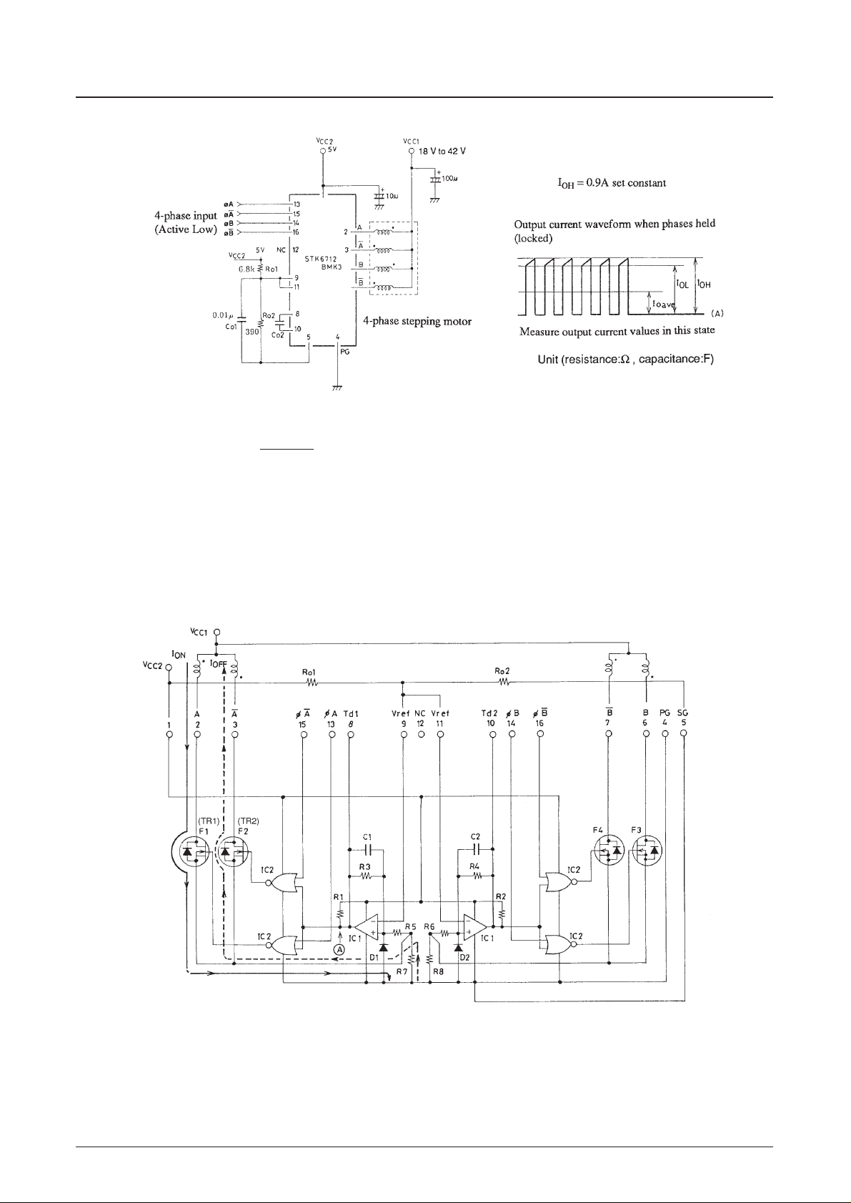
Sample Application Circuit
Note For reference, when IOH≈ 1.1 A, RO1= 6.8 kΩ and RO2= 390 Ω.
IOH= K ×
R
O2
× VCC2/R
7
RO1+R
O2
K ≈ 1.3
R7= R8≈ 0.33Ω ±3%
To reduce noise during motor hold, it is possible to mount CO1≈ 0.01 µF and CO2≈ 100 to 200 pF. Normally these are
not required.
Note Both input signals cannot be L at the same time.
STK6712BMK3 Circuit Operation
Fig. 1 STK6712BMK3 Internal Equivalent Circuit

STK6712BMK3
No. 4292-4/11
The operation for a 4-phase dual-excitation example is described below.
The STK6712BMK3 equivalent circuit is given in Fig. 1. The circuit consists of the phase drivers, the comparator, the
PWM excitation select and the current detect resistance. In Fig. 1 øA is input with low, and øA with high. When Q1
goes on, the +pin of IC1 (comparator) goes low, making IC1 output A low also. A winding current iONthrough Q1
increases as:
iON=
VCC1 – V
SAT
(1 – e
–
R
t
)·······························································································(1)
R
L
L: motor winding inductance
R: Sum of winding resistance and current detect resistance
For this reason, pin voltage VR7 at source resistor R7 increases, and when the V
RO2
voltages of pin 8 and RO2 are
equal output A goes high, and Q1 turns off. The inverse voltage VTP is as:
VTP= Vref =
R
O2
× VCC2······························································································(2)
RO1+ R
O2
In general stepping motor coils use BIFALAR windings, so the energy stored in L1 is generated by L2, at which time
the current in L2 is i
OFF
. i
OFF
conduction continues until the charges of capacitors C1 and C2 on R3 and R4 pins (EC)
equal V
R02
. When they are equal, output A inverts and becomes low. Motor winding current iONagain rises to V
RO2
level. This motor current on/off (constant current chopping) is repeated. This waveform is illustrated on the next page.
STK6712BMK3 Basic Circuit
 Loading...