How it Works
Log In / Sign Up
Buy Points
How it Works
FAQ
Contact Us
Questions and Suggestions
Users
SANYO
Loading...
S
STK4181V
STK4181X
STK4182II
STK4190K5
STK4190MK2
STK4191V
STK4191X
STK4192II
STK4199MK2
2
STK4200K5
STK4200MK2
STK4201II
STK4201V
STK4201X
STK4210K5
STK4210MK2
STK4211II
STK4211V
STK4211X
STK4220K5
STK4221II
STK4221V
STK4230K5
STK4230MK2
STK4231II
STK4231V
STK4241II
STK4241V
STK4273
STK4274
STK4332
2
STK435
STK4352
2
STK4362
STK4412
STK442-090
STK442-110
STK443-090
STK4432
STK465
STK470-070
STK490-110
STK4913
STK5321
STK5481
STK6103
STK6105
2
STK621-015
STK621-017
STK621-031
STK621-041
STK6215
STK6217
2
STK66083P
STK6711AMK4
2
STK6712AMK3
STK6712AMK4
STK6712BMK3
2
STK6712BMK4
STK6713AMK3
2
STK6713AMK4
STK6713BMK3
2
STK6713BMK4
2
STK672
STK672-010
2
STK672-020
2
STK672-040
2
STK672-050
2
STK672-080
STK672-110
STK672-120
STK673-010
2
STK6772
STK681-050
2
STK6855
STK6875
STK6877
STK730-010
STK730-020
STK730-060
STK730-080
2
STK730C
STK731B
STK732C
STK733C
stk73410
STK73410II
STK7356
STK73903
STK73904
STK73907
STK73908
STK740-441
STK740-470
STK7406
STK750-010
2
STK7560_SERIES
STK7561G
2
STK7561J
2
STK7563A
2
Loading...
Loading...
Nothing found
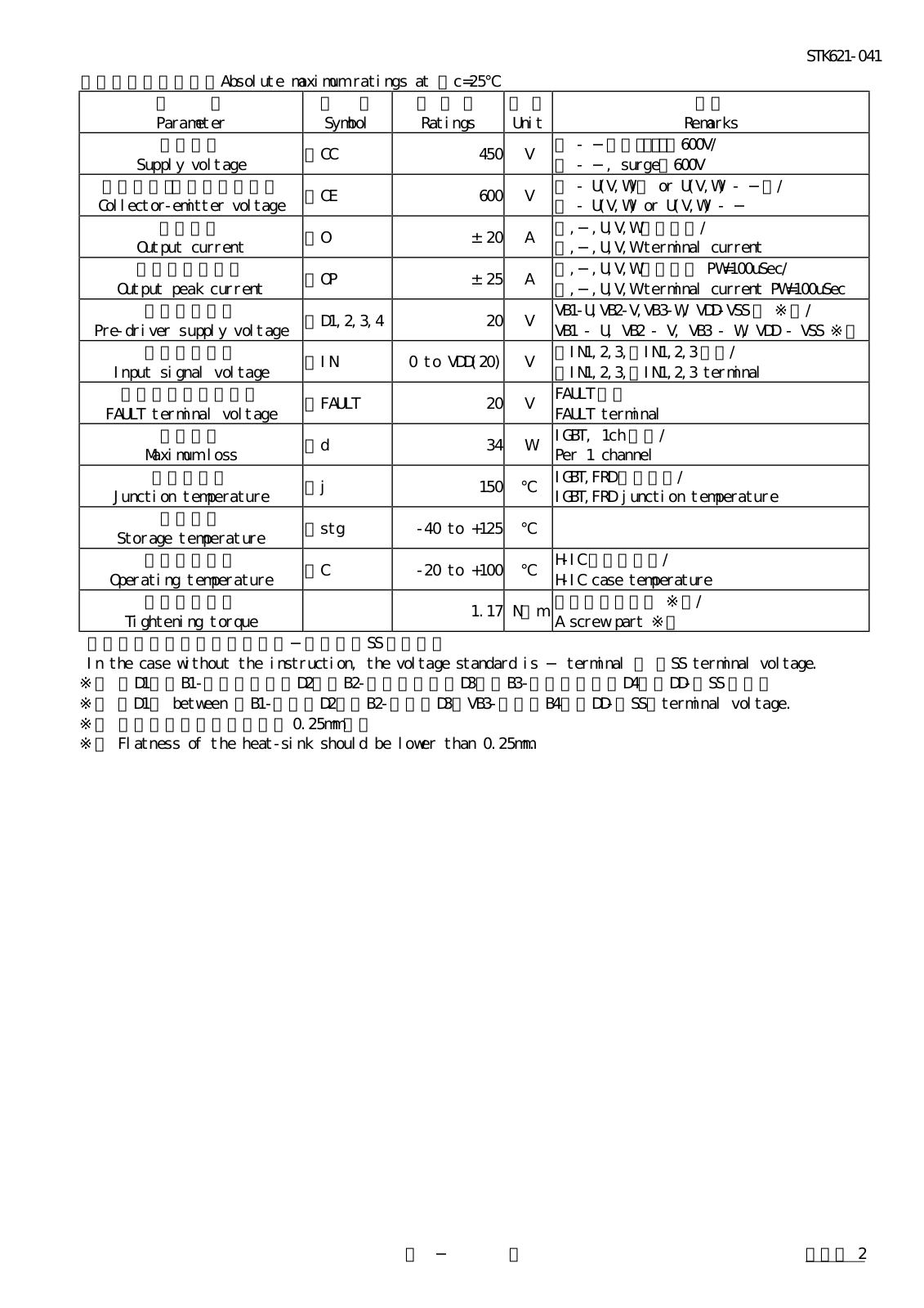
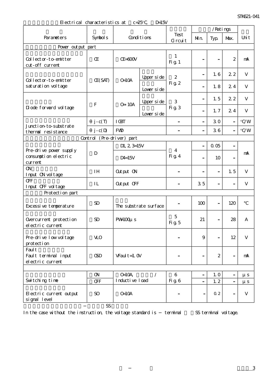
STK621-041
Service Manual
10 pgs
578.71 Kb
0
Table of contents
Loading...
SANYO STK621-041 Service Manual
...
SANYO Service Manual
Download
Specifications and Main Features
Frequently Asked Questions
User Manual
Download
Loading...
+
7
hidden pages
Unhide
You need points to download manuals.
1 point = 1 manual.
You can buy points or you can get point for every manual you upload.
Buy points
Upload your manuals
 Loading...