

Sanyo STK6105 Specifications
Overview
The STK6105 is a hybrid IC incorporating a 3-phase
brushless motor controller and driver into a single
package, on the Sanyo IMST (Insulated Metal Substrate
Technology) substrate. Revolution speed is controlled
through the DC voltage level (Vref1) external input and
PWM control of motor phase winding current. The
driver is MOSFET to minimize circuit loss and handle
high-output current (rush current) demands.
Applications
• PPC and LBP drum motors
• Air conditioner fan motors
Features
• The output driver transistor is MOSFET for low power
loss (half that of a bipolar transistor) and reliable
handling of high-output current (rush current).
• Variation in Vref1level causes the driver transistor to
switch to PWM drive for high-efficiency motor speed
variation.
• Normal and reverse revolution select function.
• Start/stop and brake functions.
• Current limiter function.
52595TH (OT) / 12793YO No. 4345-1/11
Specifications
Maximum Ratings at Ta=25°C
Allowable Operating Ranges at Ta=25°C
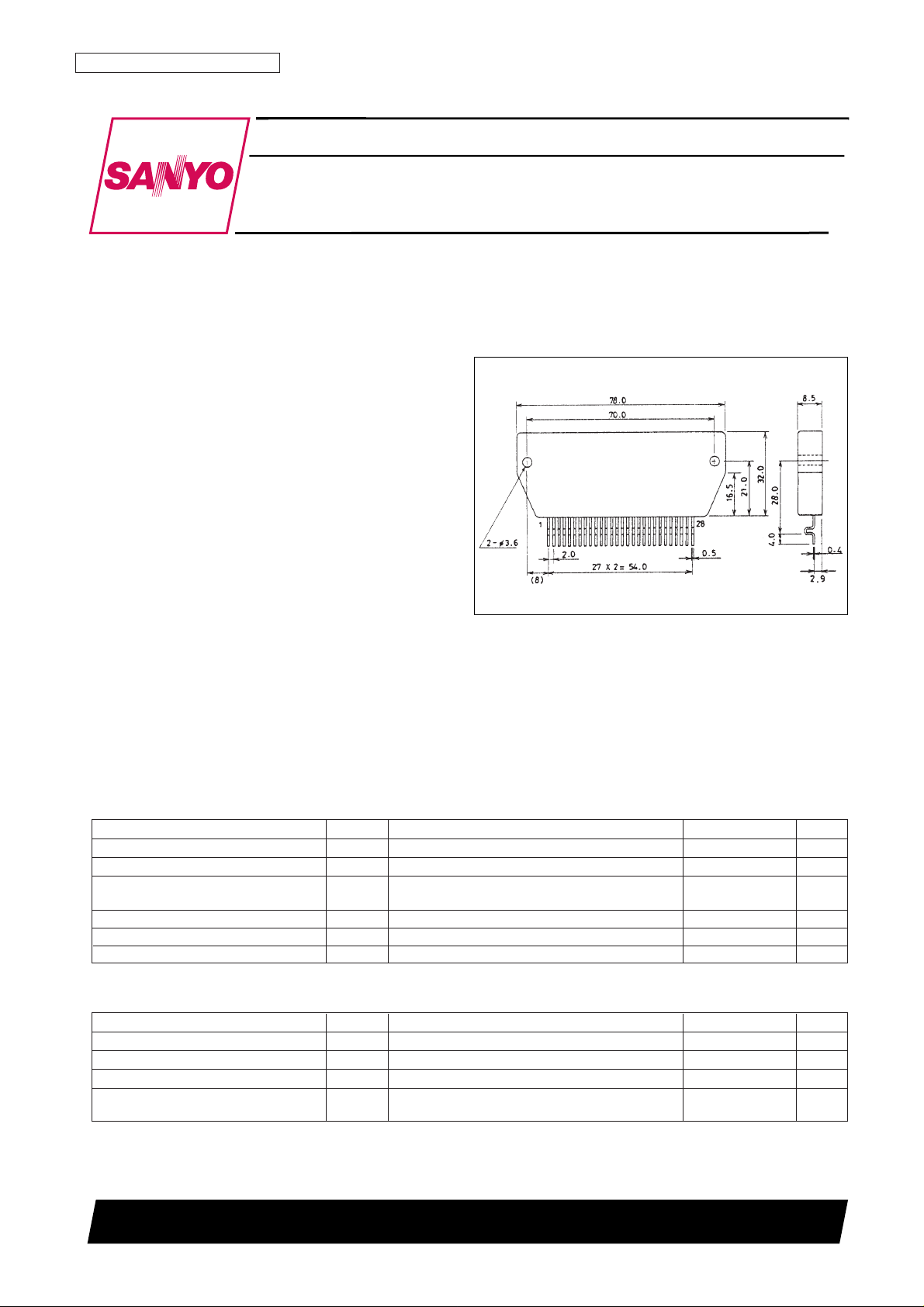
Package Dimensions
unit: mm
4130
[STK6105]
Thick Film Hybrid IC
Ordering number : EN4345A
STK6105
SANYO Electric Co.,Ltd. Semiconductor Bussiness Headquarters
TOKYO OFFICE Tokyo Bldg., 1-10, 1 Chome, Ueno, Taito-ku, TOKYO, 110-8534 JAPAN
DC 3-phase Brushless Motor Driver
(Output Current 5A)
Parameter Symbol Conditions Ratings Unit
Maximum supply voltage 1 V
CC
1 max No input signal 50 V
Maximum supply voltage 2 V
CC
2 max No input signal 7 V
Maximum output current Io max
Position detect input signal cycle = 30 ms,
8A
PWM duty = 50%, operation time 1s
Operating substrate temperature Tc max 105 °C
Junction temperature Tj max 150 °C
Storage temperature Tstg -40 to +125 °C
Parameter Symbol Conditions Ratings Unit
Supply voltage 1 V
CC
1 With input signal 16 to 42 V
Output current Io ave DC phases present 5 A
Supply voltage 2 V
CC
2 With input signal 4.75 to 6.00 V
Brake current I
OB
80 Hz full sine waves (all phases).
11 A
Operating time 0.1 s, duty = 5% (see Note 1).
Electrical Characteristics at Tc=25°C, VCC1 = 24V, VCC2 = 5.0V
Parameter Symbol Conditions
Ratings
min typ max
Unit
Supply current 1 (pin 13) I
CCO
1 CW revolution 12 20 mA
Supply current 2 (pin 13) I
CCO
2 Braking 26 38 mA
Output saturation voltage 1 Vst1 V
CC
1 sideTR, Io = 5A 0.70 0.91 V
Output saturation voltage 2 Vst2 GND sideTR, Io = 5A 0.85 1.11 V
Internal MOSFET diode forward
V
F
IF= 5A 1.0 1.5 V
voltage
PWM oscillation frequency f
C
20 25 30 kHz
Current limiter reference voltage Vref2 0.78 0.83 0.88 V
Position detect input sensitivity V
H
20 500 mV
Position detect common mode range CMRH 2.0 4.5 V
Input “L” current 1 (pins 2,3) I
IL1
V
IL1
= GND 130 200 µA
Input “L” voltage 1 (pins 2,3) V
IL1
1.0 V
Input “L” current 2 (pin 4) I
IL2
V
IL2
= GND 570 910 µA
Input “L” voltage 2 (pin 4) V
IL2
1.0 V
Vref
1
“H” voltage Vref
1H
GND side transistor not in PWM 2.82 3.20 V
Vref1“L” voltage Vref
1L
GND side transistor off 0.15 0.35 V
Zener voltage V
Z
5.7 6.2 6.7 V
FG output current I
FGH
VFG= 1.6V 80 µA
FG output “L” voltage V
FGL
IFG= 0.3mA 0.4 V
FG output pulse width t
FG
CF= 0.1µF, RF= 10kΩ 0.9 1.0 1.1 ms
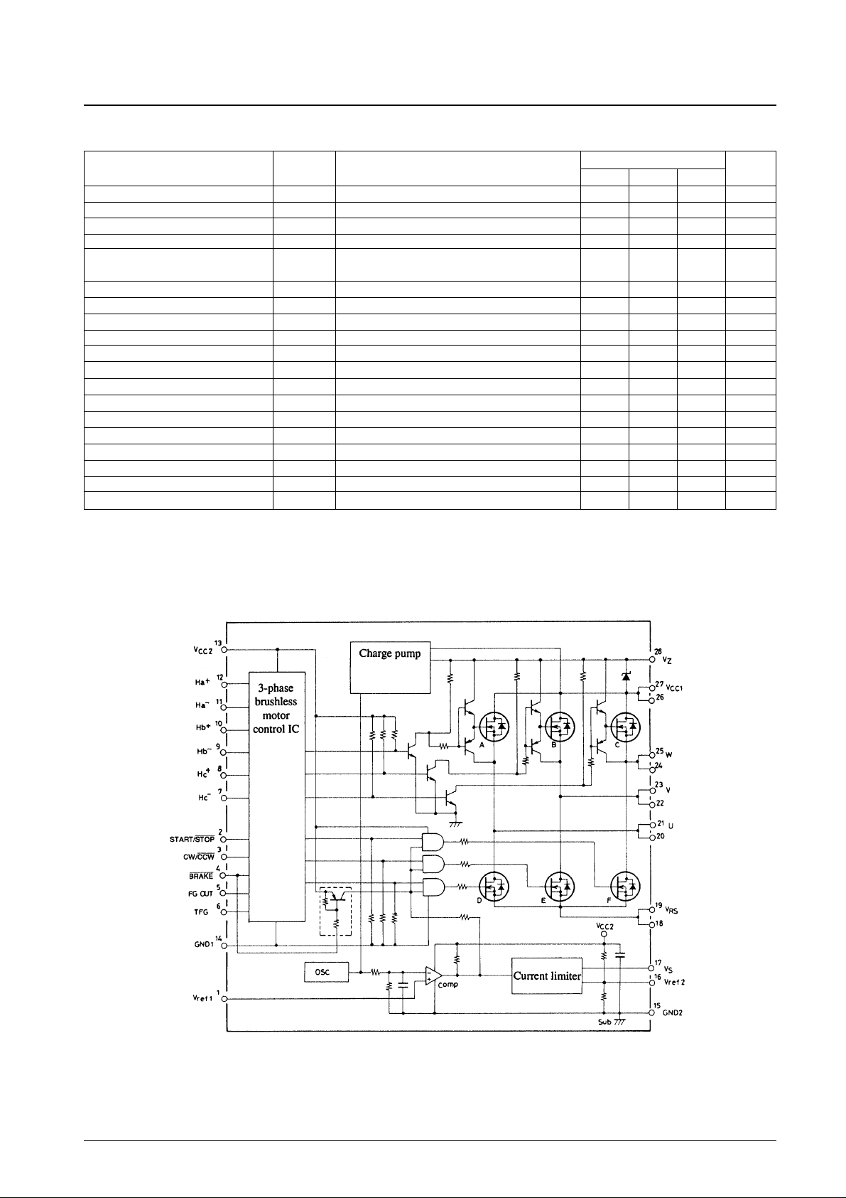
Equivalent Circuit
STK6105
No. 4345--2/11
Pin Functions
Pin No. Symbol Function
1 Vref
1
GND-side driver transistor PWM control pin; range 0.15 to 3.2V
2 START/STOP “H” = start, “L” = stop (all transistors off)
3 CW/CCW “H” = CW, “L” = CCW
4 BRAKE “H” = rotate, “L” = Only GND-side transistor on
5 FG OUT Position detect signal: output 6 pulses per cycle
6 TFG For setting FG OUT “L” level pulse width. R
F
and CFpins.
7 H
C–
Motor position detect signal input pin (to Hall device)
8 H
C+
Motor position detect signal input pin (to Hall device)
9 H
b–
Motor position detect signal input pin (to Hall device)
10 H
b+
Motor position detect signal input pin (to Hall device)
11 H
a–
Motor position detect signal input pin (to Hall device)
12 H
a+
Motor position detect signal input pin (to Hall device)
13 VCC2 Motor controller supply voltage pin
14 GND1 Motor controller IC GND pin; signal gnd (SG)
15 GND2 External R
S
GND-side connection pin; power gnd (PG)
16 Vref
2
Current limiter set pin; 0.167VCC2 when open.
17 V
S
External RScurrent limiter detect pin
18, 19 V
RS
External RSconnect pin
20, 21 U Output pin (to motor winding)
22, 23 V Output pin (to motor winding)
24, 25 W Output pin (to motor winding)
26, 27 V
CC
1 Supply voltage pin (to motor)
28 V
Z
Zener voltage (6.2V typ) for VCC1 driver transistor date source supply
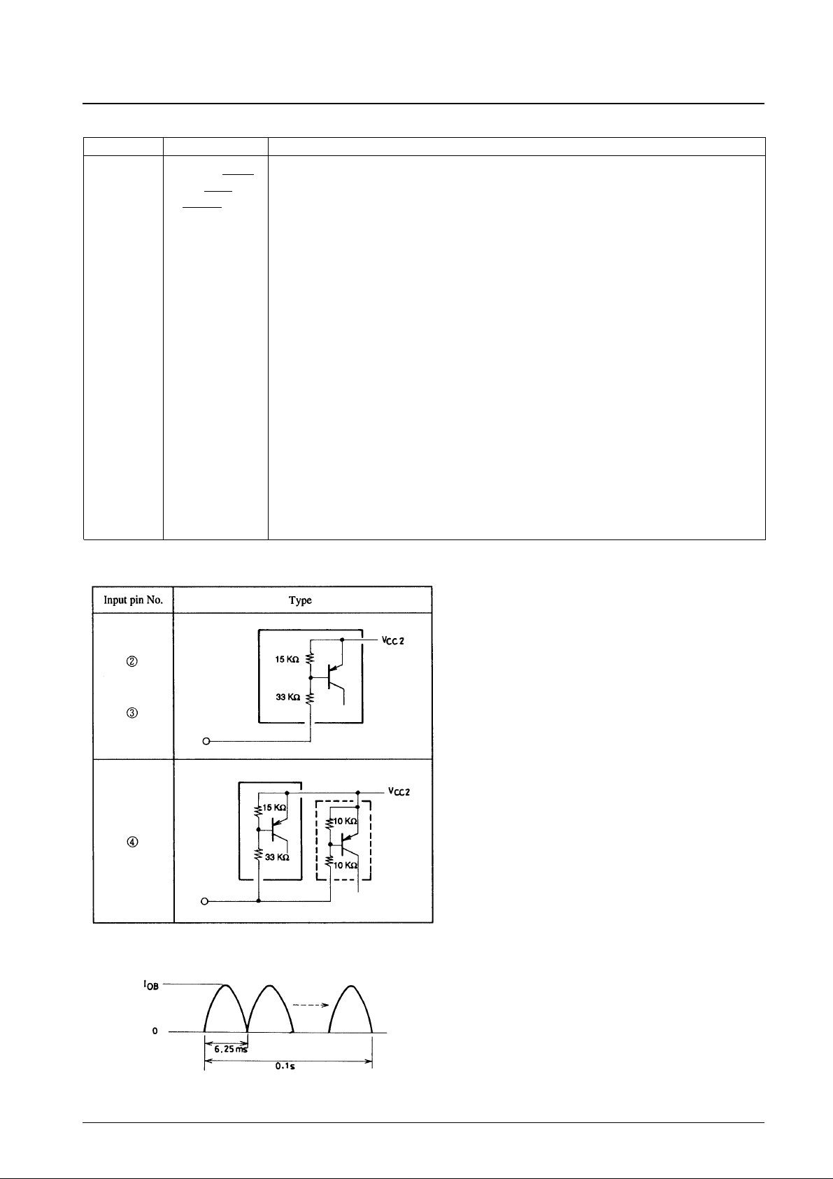
Input Type
Note 1: IOBindicates the operating current waveform peak as shown below.
STK6105
No. 4345--3/11
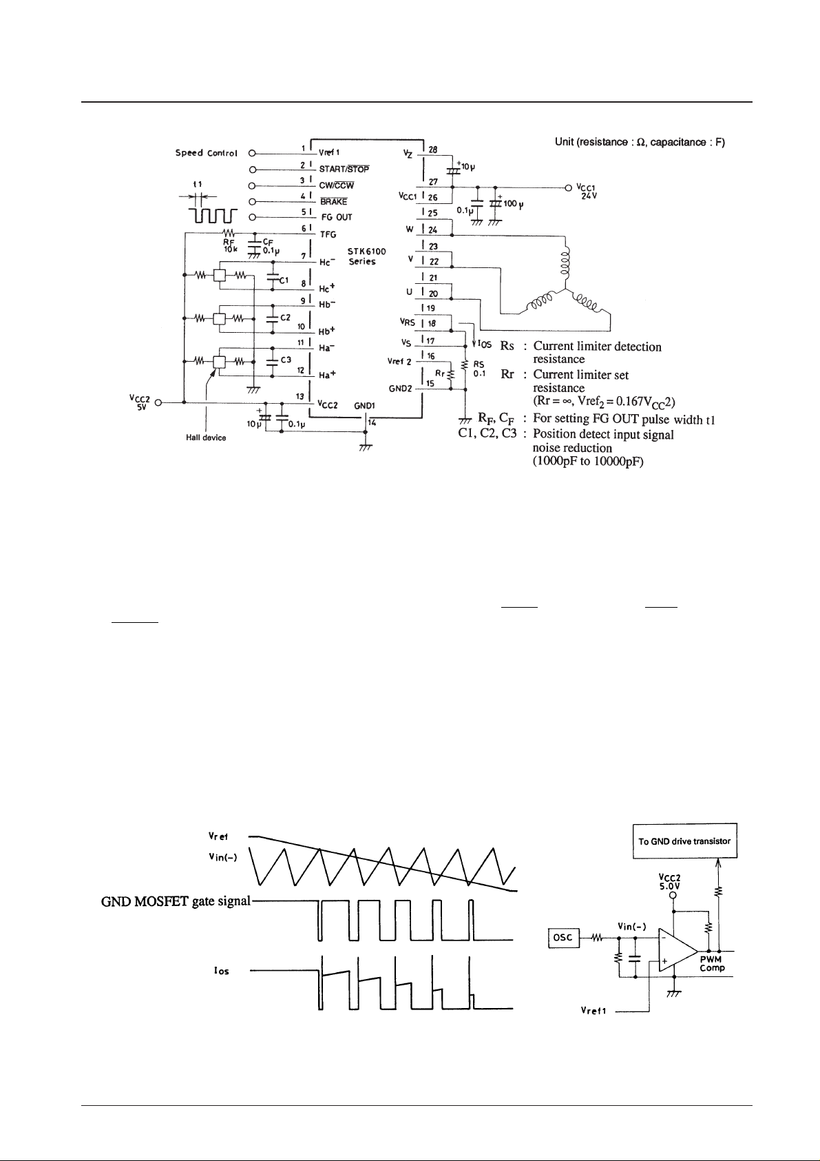
Sample Application Circuit
Description of Operation
The DC 3-phase brushless motor generally uses a permanent magnet for the rotor and places the stator coil around it.
When the rotor and stator coil are excited, magnetic force is generated between the poles, which is used for revolution
torque. For efficient revolution it is necessary to know precisely where the rotor pole is in relation to the stator pole. In
the brushless motor Hall devices and Hall ICs are widely used for this purpose, by detecting the electric power generated
along the lines of magnetic force.
(1) Motor rotating force
The block diagram for this HIC is given in Fig. 2.
The conditions before input of VCC1, with VCC2 on, are START/STOP pin H level, CW/CCW pin H level,
BRAKE pin H level and Vref1pin (speed control input) H level. The position detect signal at this time, due to the
effect of the rotor magnetic field, will be output signals from 1 or 2 devices (of the 3) so that HX+>HX–is input to
HIC pins 7-12. The signals input to pins 7-12 are input to the motor controller and converted into signals
compatible with 3-phase brushless motor revolution. When VCC1 is supplied the charge pump circuit activates,
generating VCC1 MOSFET gate voltage VZ. This outputs excitation current to the motor phase windings as
indicated in the timing chart (Fig. 3), and rotating the motor.
For revolution speed control, the Vref1pin voltage is converted and used for PWM drive to increase GND
transistor efficiency, controlling the conduction of motor current Io (Fig. 1). Control of Io means control of power
supplied to the motor, which controls motor rpm. In general motor rpm N is proportional to the PWM on duty
(when motor load is constant). The PWM on duty is proportional to the size of Vref1(see Fig. 13), and the relation
of N is as outlined below.
Ν ∝ PWM ON Duty ∝ Vref
1
Fig.1 PWM Drive Principle
STK6105
No. 4345--4/11
 Loading...