

SANYO STK4036XI Datasheet
Thick Film Hybrid IC
Ordering number : EN4620A
N3096HA (OT)/O2093YO 5-2188 No. 4620-1/5
SANYO Electric Co.,Ltd. Semiconductor Bussiness Headquarters
TOKYO OFFICE Tokyo Bldg., 1-10, 1 Chome, Ueno, Taito-ku, TOKYO, 110 JAPAN
AF Power Amplifier (Split Power Supply)
(50 W min, THD = 0.008%)
STK4036XI
Features
• Compact packaging supports slimmer set designs
• Series designed from 50 up to 150 W and pincompatibility
• Simpler heat sink design facilitates thermal design of
slim stereo sets
• Current mirror circuit, cascade circuit and purecomplimentary circuit application reduce distortion to
0.008 %
• Supports addition of electronic circuits for thermal
shutdown and load-short protection circuit as well as
pop noise muting which occurs when the power supply
switch is turned on and off.
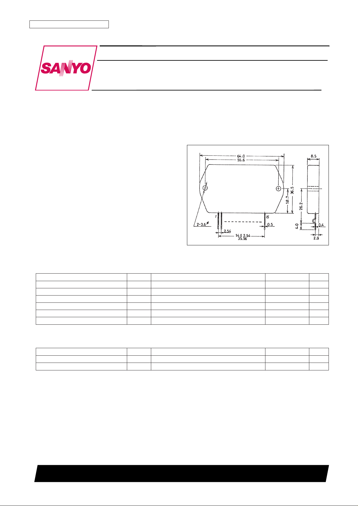
Package Dimensions
unit: mm
4075
Specifications
Maximum Ratings at Ta = 25°C
Recommended Operational Conditions at Ta = 25°C
Parameter Symbol Condition Rating Unit
Maximum supply voltage V
CC
max ± 53.5 V
Thermal resistance
θj-c 1.8 °C/W
Junction temperature Tj 150 °C
Operating substrate temperature Tc 125 °C
Storage temperature Tstg –30 to +125 °C
Available time for load shorted t
s
*1
V
CC
= ± 37 V, RL = 8 Ω, f = 50 Hz, PO = 50 W 1 s
Parameter Symbol Condition Rating Unit
Recommended supply voltage V
CC
±37 V
Load resistance R
L
8 Ω
[STK4036XI]
Operating Characteristics
at Ta = 25°C, VCC= ± 37 V, RL= 8 Ω, VG = 40 dB, Rg = 600 Ω, 100 k LPF ON, RL(non-inductive)
Note: Use rated power supply for test unless otherwise specified.
*1 When measuring permissible load short time and output noise voltage use transformer power supply indicated below.
*2 Output noise voltage represents the peak value on the rms scale (VTVM). The noise voltage waveform does not include the pulse noise.
Specified Transformer Power Supply
(MG-200 Equivalent)
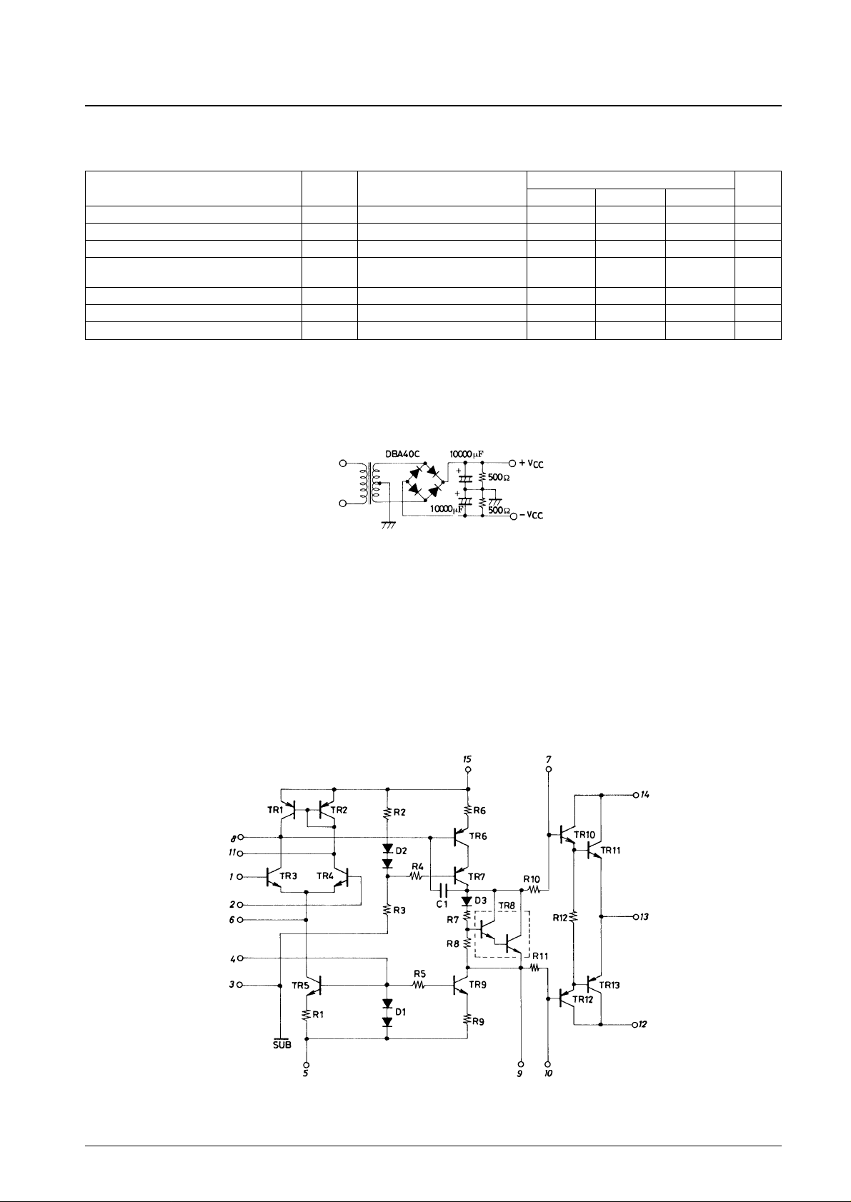
Equivalent Circuit
No. 4620-2/5
STK4036XI
Parameter Symbol Condition
Rating
Unit
min typ max
Quiescent current I
CCO
V
CC
= ± 44.5 V 15 120 mA
Output power P
O
THD = 0.008 %, f = 20 Hz to 20 kHz 50 W
Total harmonic distortion THD P
O
= 1.0 W, f = 1 kHz 0.008 %
Frequency response f
L
, f
H
PO = 1.0 W, dB 20 to 50k Hz
Input resistance r
i
PO= 1.0 W, f = 1 kHz 55 kΩ
Output noise voltage V
NO
*2
V
CC
= ± 44.5 V, Rg = 10 kΩ 1.2 mVrms
Neutral voltage V
N
VCC= ± 44.5 V –70 0 + 70 mV
+ 0
– 3
 Loading...