

SANYO STK403-430, STK403-440, STK403-450 Diagram
Ordering number : ENN7374
D2503TN (OT) No. 7374-1/8
Overview
The STK403-400 series products are audio power
amplifier hybrid ICs that consist of optimally-designed
discrete component power amplifier circuits that have
been miniaturized using SANYO's unique insulated metal
substrate technology (IMST). The adoption of a newlydeveloped low thermal resistance substrate allows this
product to integrate six power amplifier channels in a
single compact package. The adoption of a standby circuit
in this device allows it to reduce impulse noise
significantly as compared to earlier Sanyo products, in
particular, the STK402-*00 series products.
Features
• Series of pin compatible power amplifiers ranging from
30 W/ch to 45 W/ch (10%/1 kHz) devices. The same
printed circuit board can be used depending on the
output power grade.
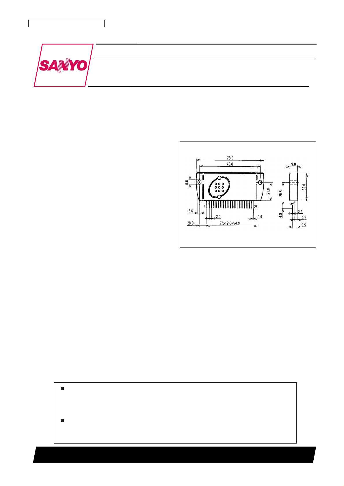
• Miniature packages
— 78.0 mm × 32.0 mm × 9.0 mm *
*: Not including the pins.
• Output load impedance: RL= 6 Ω
• Allowable load shorted time: 0.3 seconds
• Supports the use of standby and muting circuits.
Package Dimensions
unit: mm
4202-SIP28
SANYO: SIP28
[STK403-430]
STK403-430
SANYO Electric Co.,Ltd. Semiconductor Company
TOKYO OFFICE Tokyo Bldg., 1-10, 1 Chome, Ueno, Taito-ku, TOKYO, 110-8534 JAPAN
Six-Channel Class AB Audio Power Amplifier IC
20 W
× 6 Channels
Thick-Film Hybrid IC
Any and all SANYO products described or contained herein do not have specifications that can handle
applications that require extremely high levels of reliability, such as life-support systems, aircraft’s
control systems, or other applications whose failure can be reasonably expected to result in serious
physical and/or material damage. Consult with your SANYO representative nearest you before using
any SANYO products described or contained herein in such applications.
SANYO assumes no responsibility for equipment failures that result from using products at values that
exceed, even momentarily, rated values (such as maximum ratings, operating condition ranges, or other
parameters) listed in products specifications of any and all SANYO products described or contained
herein.
No. 7374-2/8
STK403-430
Item
Type No.
STK403-430 STK403-440 STK403-450
Output 1 (10%/1 kHz) 30 W × 6 ch 40 W × 6 ch 45 W × 6 ch
Output 2 (0.6%/20 Hz to 20 kHz)
20 W × 6 ch 25 W × 6 ch 30 W × 6 ch
Maximum supply voltage (No signal) ±36 V ±38 V ±40 V
Maximum supply voltage (6 Ω) ±34 V ±36 V ±38 V
Recommended supply voltage (6 Ω) ±23 V ±26 V ±28 V
Package 78.0 mm × 32.0 mm × 9.0 mm
Series Organization
Specifications
Maximum Ratings at Ta = 25°C
These products are organized as a series based on their output capacity.
Operating Characteristics at Tc = 25°C, RL= 6 Ω (noninductive load), Rg = 600 Ω, VG = 30 dB
Notes: 1. 1ch drive
2. Unless otherwise noted, use a constant-voltage supply for the power supply used during inspection.
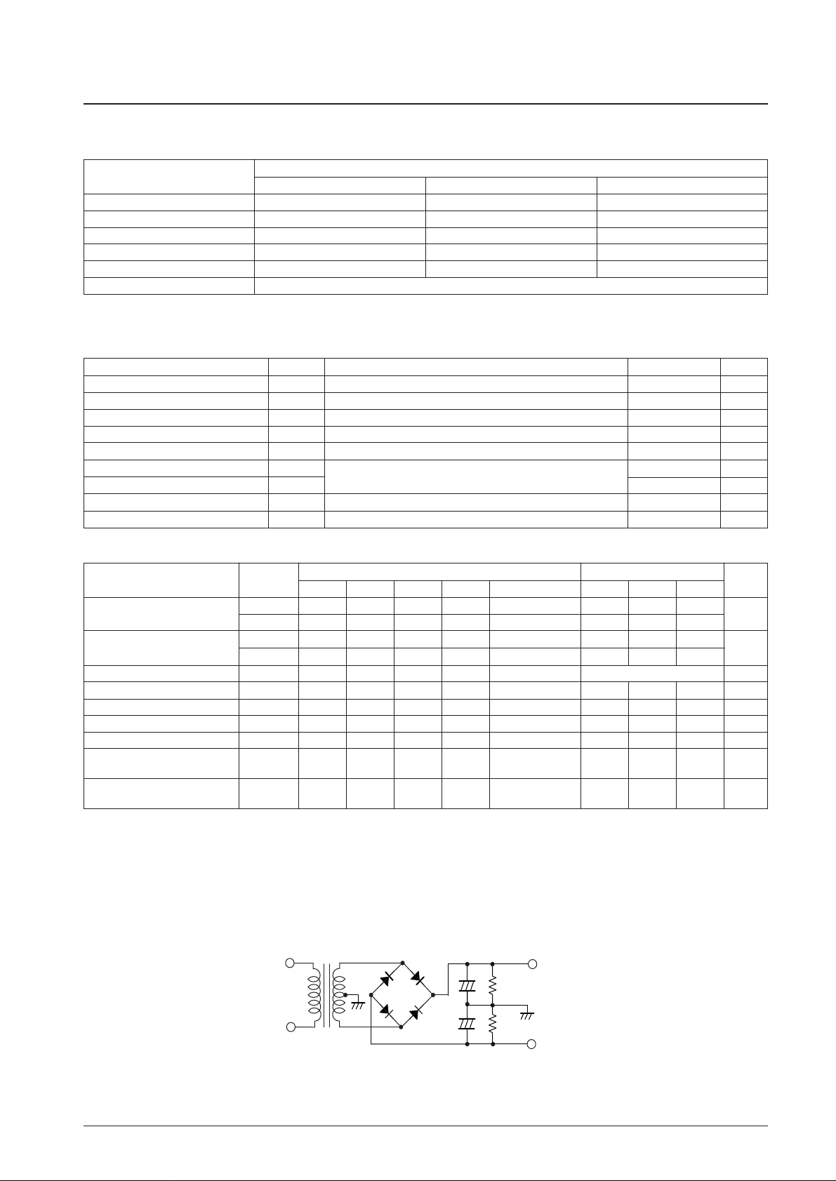
3. Use the transformer power supply circuit shown in the figure below for allowable load shorted time measurement and output noise voltage
measurement.
4. The output noise voltage values shown are peak values read with a VTVM. However, an AC stabilized (50 Hz) power supply should be used to
minimize the influence of AC primary side flicker noise on the reading.
5. Design applications so that the minus pre-V
CC
line (pin 17) is the lowest potential applied to the IC at all times.
6. A limiting resistor that assures that the maximum operating current flowing into the standby pin (pin 23) does not exceed the maximum rating must
be included in application circuits. This IC operates when a voltage higher than V
BE
(about 0.6 V) is applied to the standby pin.
4700µF
4700µF
DBA30C
500Ω
500Ω
+V
CC
--V
CC
+
+
Designated Transformer Power Supply (RP-25 equivalent)
Parameter Symbol Conditions Ratings Unit
Maximum supply voltage (No signal) V
CC
max(0) ±36 V
Maximum supply voltage V
CC
max(1) RL≥ 6 Ω ±34 V
Minimum operating supply voltage V
CC
min ±10 V
Maximum operation flow-in current (pin 23)
I
ST OFF
max 1.2 mA
Thermal resistance θ j-c Per power transistor 3.6 °C/W
Junction temperature Tj max
Both the Tj max and the Tc max conditions must be met.
150 °C
Operating IC substrate temperature Tc max 125 °C
Storage temperature Tstg –30 to +125 °C
Allowable load shorted time *
4
ts VCC= ±23.0 V, RL= 6 Ω, f = 50 Hz, PO= 20 W, 1ch drive 0.3 s
Parameter Symbol
Conditions*
1
Ratings
Unit
V
CC
(V) f (Hz) PO(W) THD (%) min typ max
P
O
(1) ±23.0 20 to 20 k 0.6 18 20
Output power *
1
PO(2) ±23.0 1 k 10 30
W
THD (1) ±23.0 20 to 20 k 5.0 VG = 30 dB 0.6
Total harmonic distortion *
1
THD (2) ±23.0 1 k 5.0 VG = 30 dB 0.03
%
Frequency characteristics f
L
, f
H
±23.0 1.0 +0 –3 dB
20 to 50 k
Hz
Input impedance ri ±23.0 1 k 1.0 55 kΩ
Output noise voltage *
2
V
NO
±28.0 Rg = 2.2 kΩ 1.0 mVrms
Quiescent current I
CCO
±28.0 No loading 60 110 180 mA
Neutral voltage V
N
±28.0 –70 0 +70 mV
Current flowing into pin 23
I
ST ON
±23.0
V23= 5 V, current Limiting
0 mA
in standby mode *
6
resistance: 6.2 kΩ
Current flowing into pin 23
I
ST OFF
±23.0 0.4 1.2 mA
in operating mode *
6
No. 7374-3/8
STK403-430
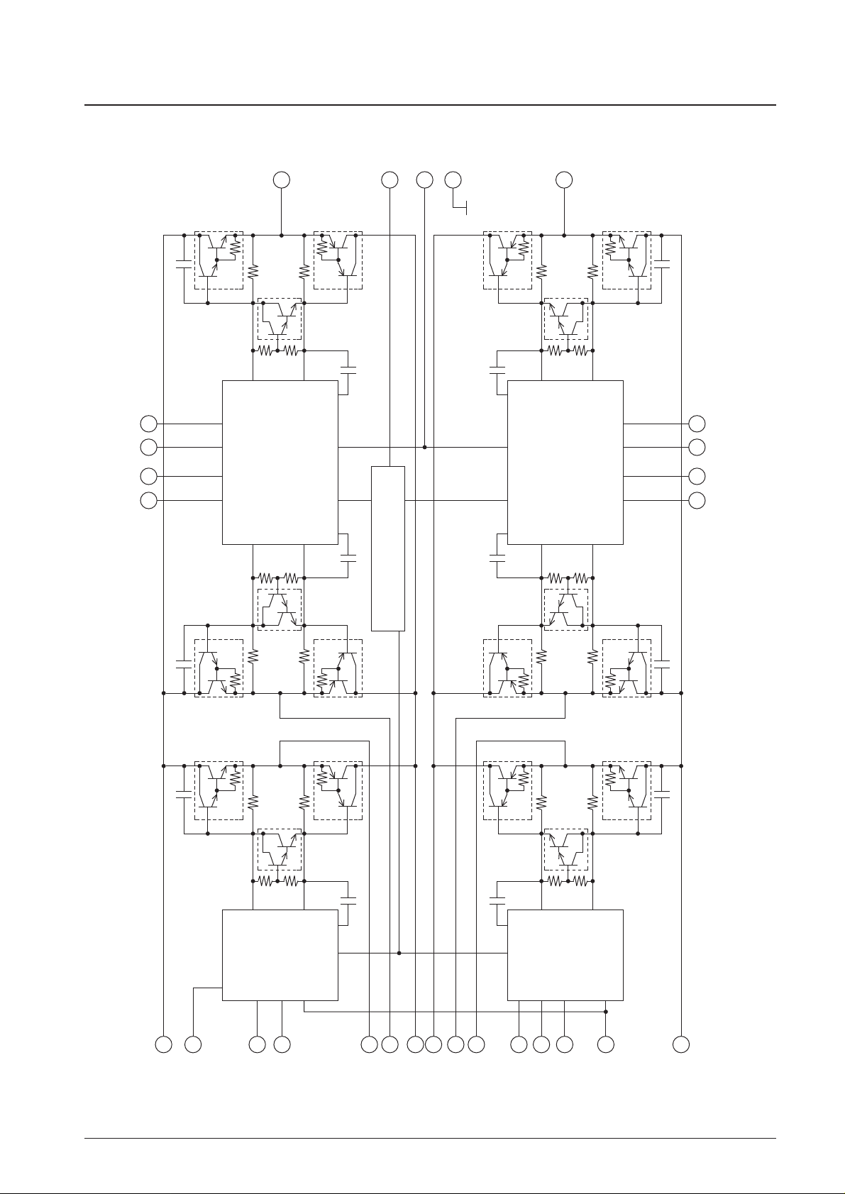
Internal Equivalent Circuit
11
5 6 7 8
9
23
19
18
2
3
4
1
10
12
13
16
15
Pre Driver IC
(CH2 / CH3)
Pre Driver IC
(CH1)
Bias Circuit
24 25 26 27
28
Pre Driver IC
(CH5 / CH6)
22
21
20
17
14
Pre Driver IC
(CH4)
ITF02247
C13
TR7
TR8
TR17
SUB
TR16
C16
C12
TR4
TR5
C15
TR13
TR14
C11
TR1
TR2
C14
TR10
TR11
TR9
R24
R25
TR6
R22
R23
TR3
R20
R21
R5
R6
R3
R4
R1
R2
TR12
R27
R26
TR15
R29
R28
TR18
R31
R30
R8
R7
R10
R9
R12
R11
C3C2
C1
C4
C5 C6
 Loading...