

Page 1
PRODUCT CODE
(ML8A) 1 122 140 00
(PL8A) 1 122 141 00
(PL8C) 1 122 141 02
(MJ8A) 1 122 136 00
(PJ8A) 1 122 137 00
(PJ8C) 1 122 137 02
REFERENCE NO. SM5110369
Chassis No. ML8-SU3200
MJ8-SU3300
NOTE: Match the Chassis No. on the unit’s
back cover with the Chassis No. in the
Service Manual.
If the Original Version Service
Manual Chassis No. does not match
the unit’s, additional Service
Literature is required.You must refer to
“Notices” to the Original Service
Manual prior to servicing the unit.
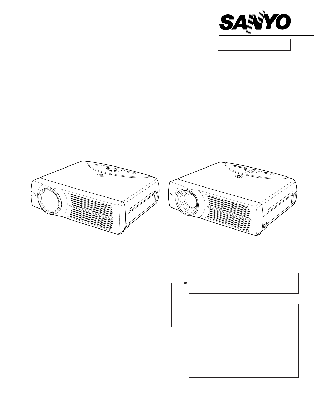
Multimedia Projector
SERVICE MANUAL
FILE NO.
Model No. PLC-SU32
PLC-SU33
U.S.A., Canada,
Europe, Asia, Africa
U.K
Original Version
PLC-SU33 PLC-SU32
Page 2

-2-
■ Contents
■ Safety instructions ________________________________________________3
■ Specifications __________________________________________________ 4
■ Adjustments after parts replacement ________________________________ 5
■ Circuit protections ______________________________________________ 6-7
● Fuse ____________________________________________________ 6
● Thermal switch ____________________________________________ 6
● Interlock switch ____________________________________________ 6
● Warning temperature and power failure protection ________________ 7
■ Mechanical disassemblies ______________________________________ 8-13
■ Optical parts disassemblies ____________________________________ 14-17
■ LCD panel/prism ass’y replacement ________________________________ 19
■ Lamp replacement ______________________________________________ 20
■ Optical adjustments __________________________________________ 21-24
● Contrast adjustment ________________________________________ 21
● Condenser lens adjustment __________________________________ 22
● Condenser lens-Out adjustment ______________________________ 23
● Relay lens-Out adjustment __________________________________ 24
■ Electric adjustments __________________________________________ 25-30
● Service adjustment menu operation ____________________________ 23
● Circuit adjustments ______________________________________ 24-29
● Service adjustment data table ______________________________ 30-33
● Test points and locations ____________________________________ 34
■ Troubleshooting ______________________________________________ 35-39
● No power ______________________________________________ 35-36
● No picture ____________________________________________ 37-38
● No sound ________________________________________________ 39
● Lens motor problems ______________________________________ 39
■ Control port functions ________________________________________ 40-43
■ Waveforms __________________________________________________ 44-45
■ Cleaning ______________________________________________________ 46
■ IC block diagrams ____________________________________________ 47-53
■ Service parts lists ____________________________________________ 54-86
● Electrical parts list ______________________________________ 54-78
● Mechanical parts list ____________________________________ 79-80
● Optical parts list ________________________________________ 81-85
Drawings & Diagrams ______________________________________ A1-A15
■ Parts description and reading in schematic diagram ____________________ A2
■ Circuit block diagram ____________________________________________ A3
■ Power supply lines ______________________________________________ A4
■ Schematic diagrams ________________________________________ A5-A11
■ Printed wiring board diagrams ________________________________ A12-A14
■ Pins description of ICs, transistors, diodes __________________________ A15
Page 3
-3-
■ Safety Instructions
WARNING:
The chassis of this projector is isolated (COLD) from AC line by using the converter transformer. Primary side of
the converter and lamp power supply unit circuit is connected to the AC line and it is hot, which hot circuit is identified with the line ( ) in the schematic diagram. For continued product safety and protection of personnel
injury, servicing should be made with qualified personnel.
The following precautions must be observed.
SAFETY PRECAUTIONS
1: An isolation transformer should be connected in the
power line between the projector and the AC line
before any service is performed on the projector.
2: Comply with all caution and safety-related notes pro-
vided on the cabinet back, cabinet bottom, inside the
cabinet or on the chassis.
3: When replacing a chassis in the cabinet, always be
certain that all the protective devices are installed
properly, such as, control knobs, adjustment covers
or shields, barriers, etc.
DO NOT OPERATE THIS PROJECTOR WITHOUT
THE PROTECTIVE SHIELD IN POSITION AND
PROPERLY SECURED.
4: Before replacing the cabinet cover, thoroughly
inspect the inside of the cabinet to see that no stray
parts or tools have been left inside.
Before returning any projector to the customer, the
service personnel must be sure it is completely safe to
operate without danger of electric shock.
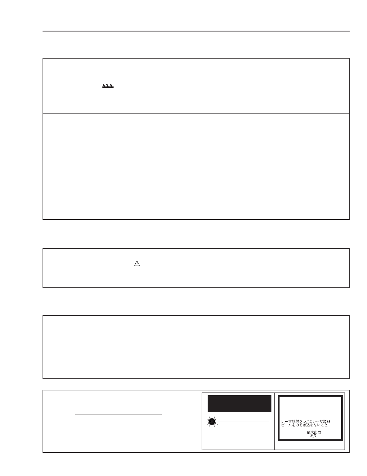
SERVICE PERSONNEL WARNING
Eye damage may result from directly viewing the light produced by the Lamp used in this equipment. Always turn
off Lamp before opening cover. The Ultraviolet radiation eye protection required during this servicing.
Never turn the power on without the lamp to avoid electric-shock or damage of the devices since the stabilizer
generates high voltages(15kV - 25kV) at its starts.
Since the lamp is very high temperature during units operation replacement of the lamp should be done at least
45 minutes after the power has been turned off, to allow the lamp cool-off.
PRODUCT SAFETY NOTICE
Product safety should be considered when a component replacement is made in any area of the projector.
Components indicated by mark in the parts list and the schematic diagram designate components in which
safety can be of special significance. It is, therefore, particularly recommended that the replacement of there parts
must be made by exactly the same parts.
DO NOT ATTEMPT TO SERVICING THE
REMOTE CONTROL UNIT.
Laser Beam may be leaked out when in disassemble
the Unit. As the Laser Beam used in this Remote control unit is harmful to the eyes.
LASER RADIATION
DO NOT STARE INTO BEAM
MAX. OUTPUT: 1mW
WAVE LENGTH: 650 ±20nm
CLASS
II LASER PRODUCT
This product is complied with 21 CFR
part 1040.10
CAUTION
LASER RADIATION
DO NOT STARE INTO BEAM
CLASS 2 LASER PRODUCT
LASER-STRAHLING
NICHT IN DEN STRAHL BLICKEN
LASER KLASSE 2
IEC60825-1, Am. 1 1997
MAX OUTPUT ( ) : 1 mW
WAVE LENGTH ( ) : 650±20nm
Page 4
-4-
Projector Type Multi-media Projector
Dimensions (W x H x D) 13.11” x 3.52” x 9.96” (333mm x 89.5mm x 253mm)
Net Weight 9.3 lbs (4.2 kg) (PLC-SU32), 9.8 lbs (4.4 kg) (PLC-SU33)
LCD Panel System 0.9” TFT Active Matrix type, 3 panels
Panel Resolution 800 x 600 dots
Number of Pixels 1,440,000 (800 x 600 x 3 panels)
Color System 6 color system (PAL, SECAM, NTSC, NTSC4.43, PAL-M and PAL-N)
High Definition TV SIgnals 480i, 480p, 575i, 575p, 720p. 1035i and 1080i
Scanning Frequency H-sync. 15 ~ 80kHz, V-sync. 50 ~ 100Hz
Projection Image Size (diagonal) Adjustable from 31” to 300” (PLC-SU32)
Adjustable from 34” to 300” (PLC-SU33)
Horizontal Resolution 800 TV lines
Projection Lens F 1.7 ~ 2.0 lens with f 37.4mm ~ 48.3mm with motor zoom and focus (PLC-SU32)
F 1.9 ~ 2.1 lens with f 21.3mm ~ 25.6mm with motor zoom and focus (PLC-SU33)
Throw Distance 5.3’ ~ 40.0’ (1.6m ~ 12.2m) (PLC-SU32)
3.0’ ~ 22.6’ (0.9m ~ 6.9m) (PLC-SU33)
Projection Lamp 200watts
Video Input Jacks RCA Type x 3 (Video/Y, Cb/Pb, Cr/Pr) and Mini DIN 4 pin x 1(S-Video)
Audio Input Jacks RCA Type x 2
Computer Input Terminal DVI-I Terminal (Digital/Analog)
Monitor Output Terminal (VGA) HDB15 Terminal x 1
Computer Audio Input Jack Mini Jack (stereo)
Control Port Connector Mini DIN 8 pin x 1
USB Connector USB Series B receptance x 1
Audio Output Jacks RCA Type x 2
Internal Audio Amp. 1.0watt RMS (monaural)
Built-in Speaker 1 speaker, 1.18” x 1.57” (30mm x 40mm)
Feet Adjustment 0˚ to 15.6˚
Voltage and AC 100 ~ 120V (3.6A Max. Ampere), 50/60Hz (The U.S.A and Canada)
Power Consumption AC 200 ~ 240V (1.8A Max. Ampere), 50/60Hz (Continental Europe and the U.K)
Operating Temperature 41˚F ~ 95˚F (5˚C ~ 35˚C)
Storage Temperature 14˚F ~ 140˚F (-10˚C ~ 60˚C)
Remote Control Transmitters Wireless Remote Control, batteries AA, UM3 or R06 Type x 2
■ Specifications
● The specifications are subject to change without notice.
This symbol on the nameplate means the product is Listed by Underwriters
Laboratories Inc. It is designed and manufactured to meet rigid U.L. safety standards against risk of fire, casualty and electrical hazards.
Page 5
-5-
Condenser lens adjustment ❍●
Condenser lens-out adjustment ❍●
Relay lens-out adjustment ❍●
Contrast Adjustment
R-Contrast adjustment ●
G-Contrast adjustment ●
B-Contrast adjustment ●
Output voltage adjustment ●
Fan voltage adjustment ●
Pedestal adjustment ●
NRS adjustment ●
Signal center adjustment ●
Black level adjustment ●
PC offset adjustment ●
PC gain adjustment ●
AV gain adjustment ●
Common center adjustment ● ●
Gamma shift adjustment ❍ ●
White balance adjustment ❍ ❍
Disassembly / Replaced Parts
LCD/
Prism
Ass’y
Condenser
Lens
Polarized glass
RGB
Optical Adjustments
Electrical Adjustments
● : Adjustment necessary ❍ : Check necessary
P. F .
Board
Main
Board
Condenser
Lens-Out
■ Adjustments after Parts Replacement
Relay
Lens-Out
Power
Board
Page 6
-6-
● Interlock switch
The interlock switch (SW904) cuts off the AC mains power supply
when the lamp cover is removed. After opening the lamp cover for
replacing the lamp ass’y, place the lamp cover correctly otherwise
the projector can not turn on.
● Thermal switch
There is the thermal switch (SW902) inside of the projector to
prevent the internal temperature from rising abnormally. When the
internal temperature reaches near 100˚C, turn off the AC main
power supply automatically.
The thermal switch is not reset to normal automatically even if the
internal temperature becomes normal. Reset the thermal switch
following procedure.
Check the resistance between terminals of thermal switch by
using the tester. If it has high impedance, thermal switch may be
in operative.
How to reset the thermal switch
1.
Remove the cabinet top following to “Mechanical
Disassemblies”.
2. Press the reset button on the thermal switch.
CAUTION:
Before press the reset button, disconnect the AC cord from the
projector.
■ Circuit Protections
This projector is equipped with the following circuit protections to operate in safety. If the abnormality occurs inside
the projector, it will automatically turn off by operating one of the following protection circuits.
● Fuse
The fuse is located inside of the projector. When either the LAMP
indicator or the READY indicator is not illuminated, fuse may be
opened. Check the fuse as following steps.
It should be used the specified fuse as follows;
How to replace the fuse
1. Remove the cabinet top following to “Mechanical
Disassemblies”.
2. Remove the fuse from fuse holder.
To install the fuse, take reversed step in the above.
Fuse Part No.: 423 022 2102
TYPE T4.0AH 250V FUSE
LITTLE FUSE INC. TYPE 215004
Fuse
Thermal switch (SW902)
Reset Button
Line Filter Board
Page 7
-7-
Circuit Protections
● Warning temperature and power failure protection
The TEMP WARNING indicator flashes red and the projector will automatically turn off when the internal temperature of the projector exceeds the normal temperature or when stopping cooling fans or when the internal power
supply lines are failed.
Check the following possible causes and wait until stopping the TEMP WARNING indicator flashing.
Possible causes
- Air filter is clogged with dust particles. Remove dust from the air filter by following instructions in the “Air filter
care and cleaning” below.
- Ventilation slots of the projector are blocked. In such an event, reposition the projector so that ventilation slots are
not obstructed.
- Check if projector is used at higher temperature place (Normal operating temperature is 5 to 35 ˚C or 41 to 95˚F)
If the TEMP WARNING indicator still continues to flash, there may be defects on cooling fans or power supply circuits. Please check fan operation and power supply lines referring to the “Power Supply Lines Chart”.
Air filter care and cleaning
The removable air filter prevents dust from accumulation on the surface of the projection lens and projection mirror.
Should the air filter become clogged with dust particles, it will reduce the cooling fan’s effectiveness and may result
in internal heat build up and reduce the life of the projector.
To clean up the air filter, follow the cleaning procedure
below:
1. Turn the power off, and disconnect the AC power cord
from the AC outlet.
2. Turn the projector up side down and remove an air filter
by pulling the latches of them upward.
3. Clean the air filter with brush or wash out the dust and
particles.
4. Replace the air filter properly. Make sure that the air fil-
ter is fully inserted.
CAUTION:
Do not operate the projector with the air filter removed. The
dust is stuck on the LCD panel and the mirror, and it may
spoil the fine picture image.
Do not put the small parts into the air intake vents. It may
result in the malfunction of the projector. The air filter is
small parts. Take care that children don’t eat or swallow it.
RECOMMENDATION
We recommend to avoid dusty, smoky place for operating the projector. Using in dusty place may cause the picture
of poor quality.
When using under the dusty or smoky conditions, dust may accumulate on the LCD panel and lens inside it, and
may resultantly be projected on the screen together with the picture.
When the above symptoms are noticed, please clean up the LCD panel and lens following to the “Cleaning
Method”.
Air filter
Page 8
-8-
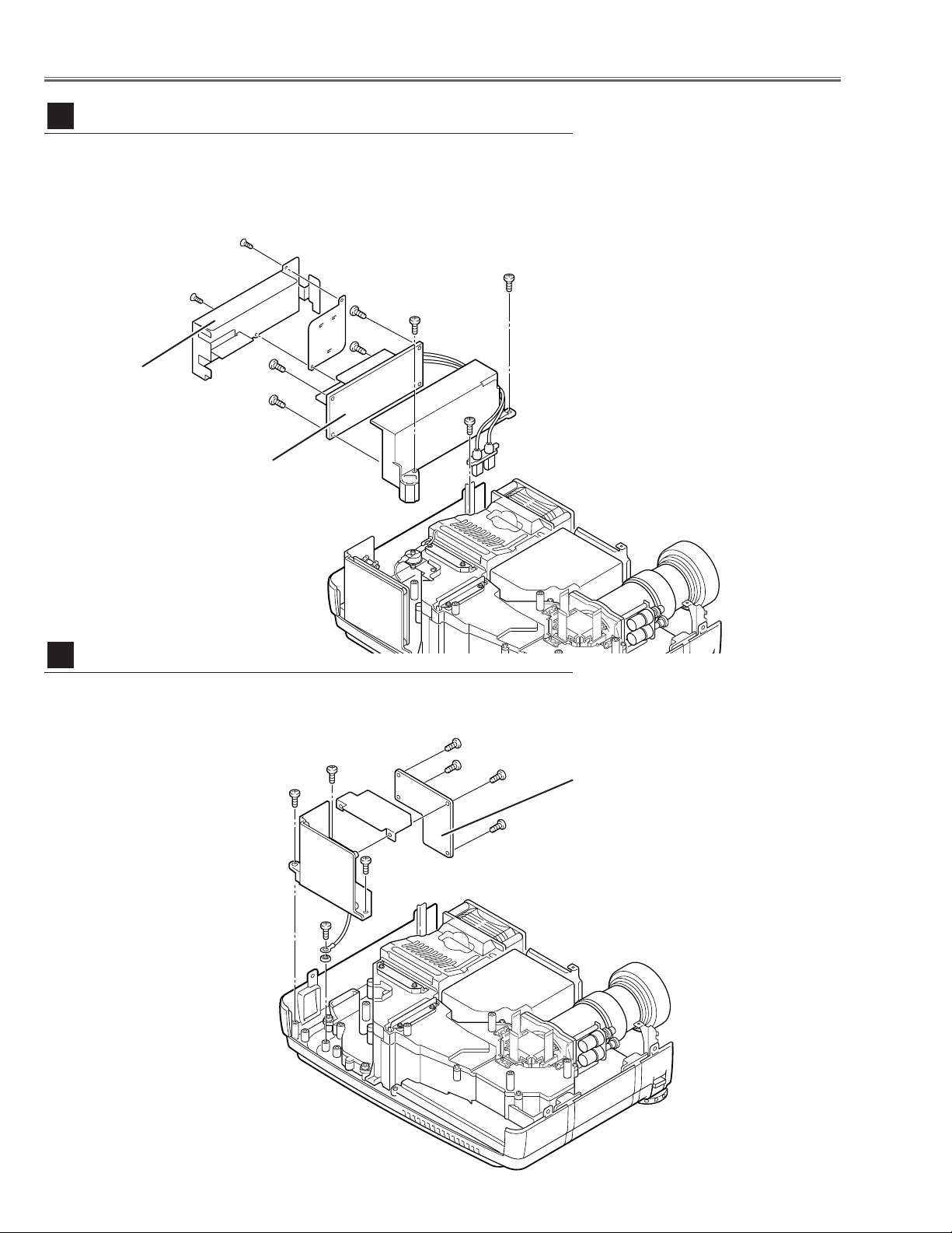
1 Remove 4 screws A to take the Cabinet Top Ass’y upward off.
2 Remove the Control Panel off from the Cabinet Top by lifting the edge of
control panel.
■ Mechanical Disassemblies
Mechanical disassemble should be made following procedures in numerical order.
Following steps show the basic procedures, therefore unnecessary step may be ignored.
Caution:
The parts and screws should be placed exactly the same position as the original otherwise it may cause loss of
performance and product safety.
Fig.1
1 Remove 8 screws to take the Main Board upward off.
Fig.2
Cabinet Top and Control Panel removal
1
Main Board removal
2
A
A
A
A
Main Board
Control panel
Cabinet top
Page 9
Temp board
-9-
Mechanical Disassemblies
1 Remove 1 screw A to release a grounding wire.
2 Pull the Rear Panel ass’y upward.
3 Remove 4 screws B and remove the AV Board.
4 Remove 4 screws C and remove the DVI Board.
5 Remove 4 screws D and remove the speaker.
6 Remove 1 screws E and remove the Temp Board..
Fig.3
Fig.4
1 Remove 4 screws A and unhook 2 hooks B at the both of left and right
side, and the take the Front Panel ass’y off.
2 Remove 1 screw C to take the R/C Board off.
AV, DVI, Temp Board and Speaker removal
3
Front Panel and R/C Board removal
4
A
B
B
B
C
A
A
A
A
B
C
DVI board
AV board
Speaker
R/C board
B
C
E
D
D
C
Page 10
-10-
Mechanical Disassemblies
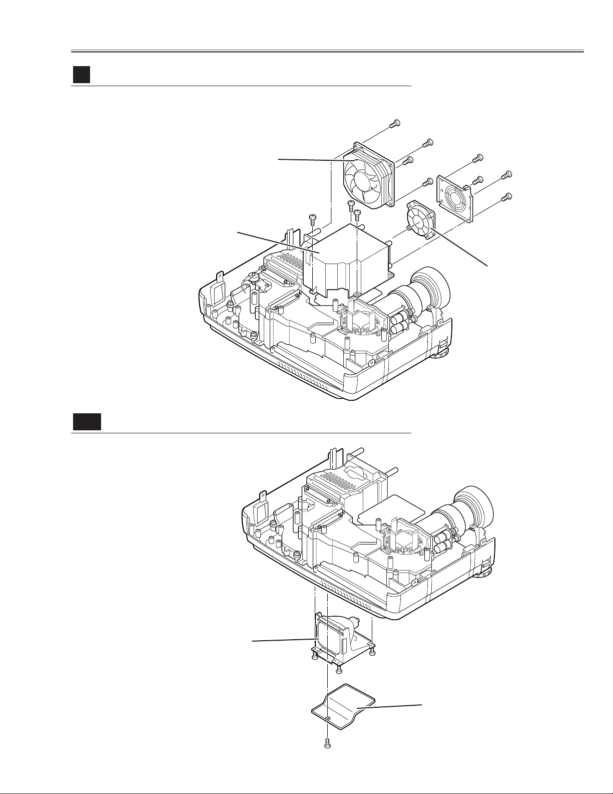
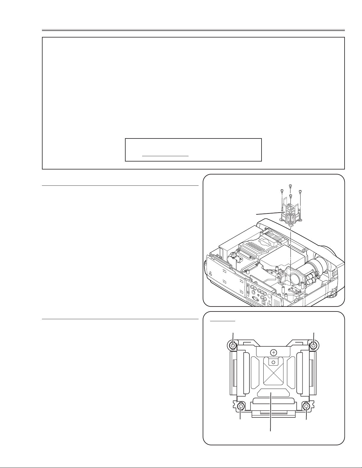
1 Remove 1 screw A and disconnect the Lamp Socket.
2 Remove 2 screws B to take the Lamp Ballast ass’y upward off.
3 Remove 2 screws C to take the isolation sheet off.
4 Remove 4 screws D to take the lamp ballast board off.
Fig.5
1
Remove 3 screws A and pull the Filter Board ass’y upward.
2 Remove 1 screw B to take the grounding lead from the cabinet bottom.
3 Remove 4 screws C to take the Filter Board off.
Fig.6
Lamp Ballast Unit removal
5
Filter Board removal
6
A
Lamp ballast board
B
B
D
D
D
D
A
A
A
B
C
C
C
C
Filter board
C
C
Isolation sheet
Page 11
-11-
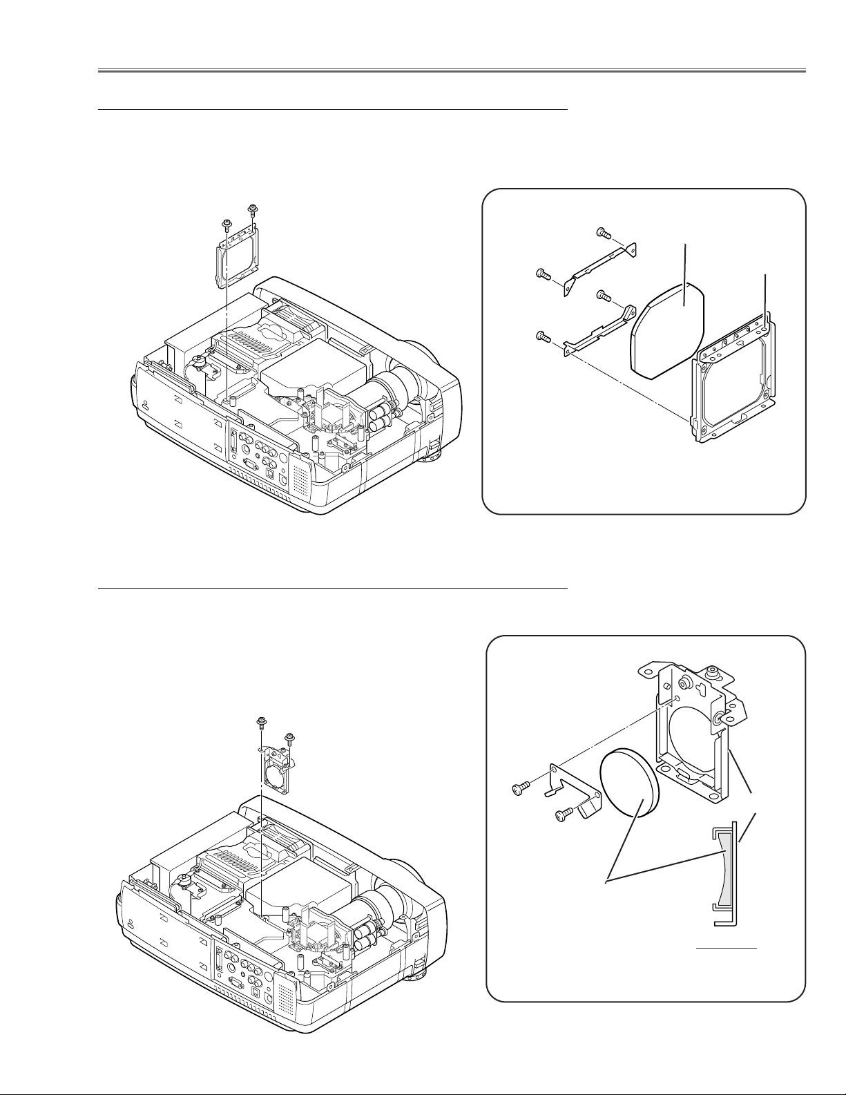
1 Remove 4 screws A to take the Fan(FN901) off.
2 Remove 4 screws B to take the Fan(FN905) off.
3 Remove 3 screws C to take the Power Box Cover upward off.
Mechanical Disassemblies
1 Remove 1 screw A to take the Lamp Cover off.
2 Loosen 3 screws B to take the Lamp assembly by
pulling the handle.
Step to next procedure.
Fig.8-1
Fig.7
Power Box Cover and Fans(FN901, FN906) removal
7
Optical Unit removal
8
-1
A
A
A
A
B
BB
B
C
C
C
FN901
FN906
Power box cover
Lamp cover
Lamp ass’y
A
B
B
B
Page 12
-12-
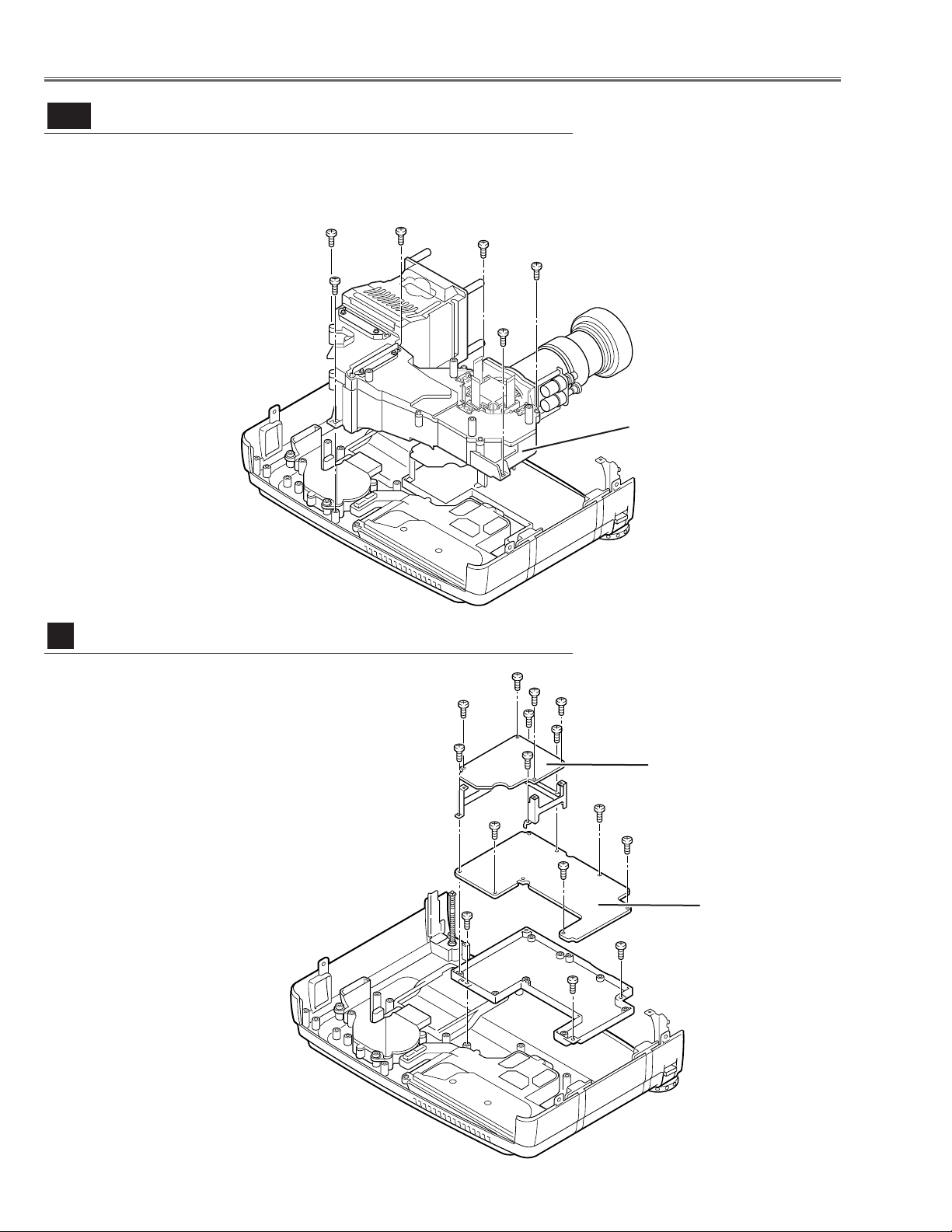
Step from previous procedure.
3 Remove 6 screws C to take the Optical Unit upward upward off.
To mount optical unit, mount optical unit first then mount the Lamp assembly
and Lamp Cover.
Mechanical Disassemblies
1 Remove 8 screws A to take the Power Board ass’y
upward off.
2 Remove 4 screws B to take the P. F. Board from the
Power Board.
3 Remove 3 screws C to take the Power Board holder
from the Cabinet Bottom.
Fig.9
Power and P.F. Board removal
9
A
Power board
A
A
A
A
A
A
A
B
B
B
B
C
C
C
P. F. board
Fig.8-2
Optical Unit removal
8
-2
Optical unit
C
C
C
C
C
C
Page 13
-13-
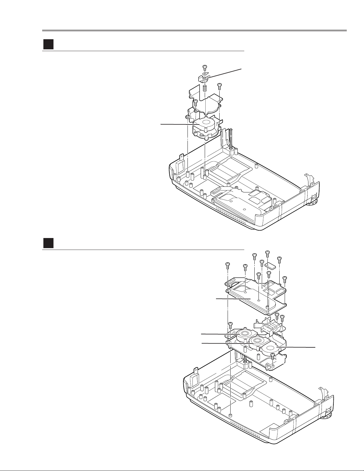
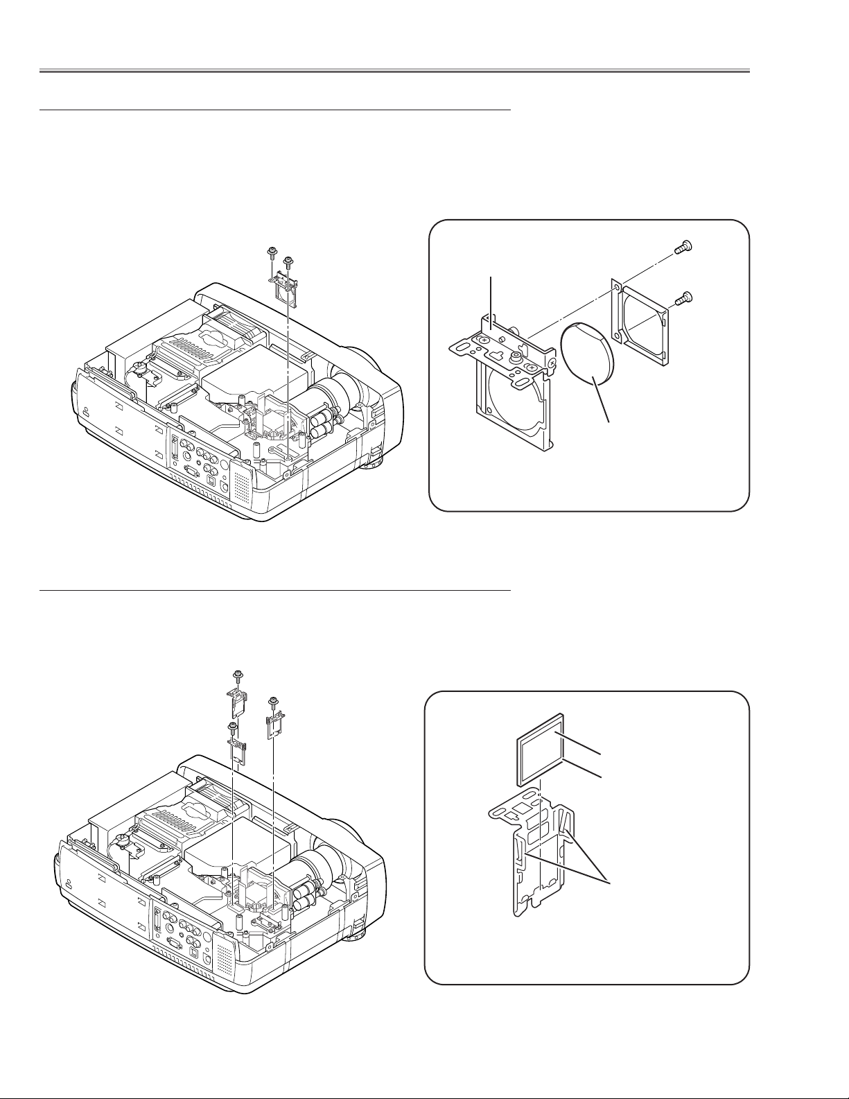
1 Remove 1 screw A and take a Washer, Spring and
Interlock Switch lever.
2 Pull the Fan and duct ass’y upward, then remove the
2 screws B to take the Fan (FN906) off.
Mechanical Disassemblies
Fig.10
1 Remove 8 screws B and to take the Fan Duct
Top off and remove the Fans (FN902, FN903,
FN904).
2 Remove 4 screws C to take the Fan Duct Bottom
off from the Cabinet Bottom.
Fig.11
Fan (FN905) removal
10
Fans (FN902, FN903, FN904) removal
11
Interlock switch lever
A
B
B
FN905
A
B
B
B
B
B
B
B
C
C
C
C
FN904
FN903
FN902
Fan duct top
Page 14
-14-
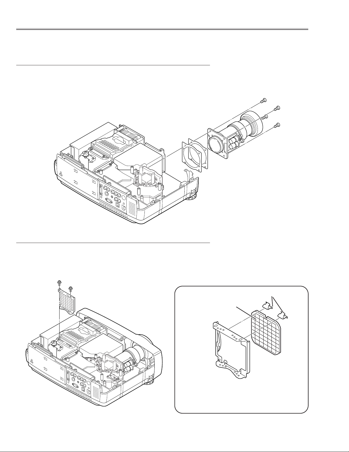
1 Remove the Front Panel following to “Front Panel Removal” on “Mechanical
Disassemblies”.
2 Remove 4 screws to take the Projection Lens ass’y off.
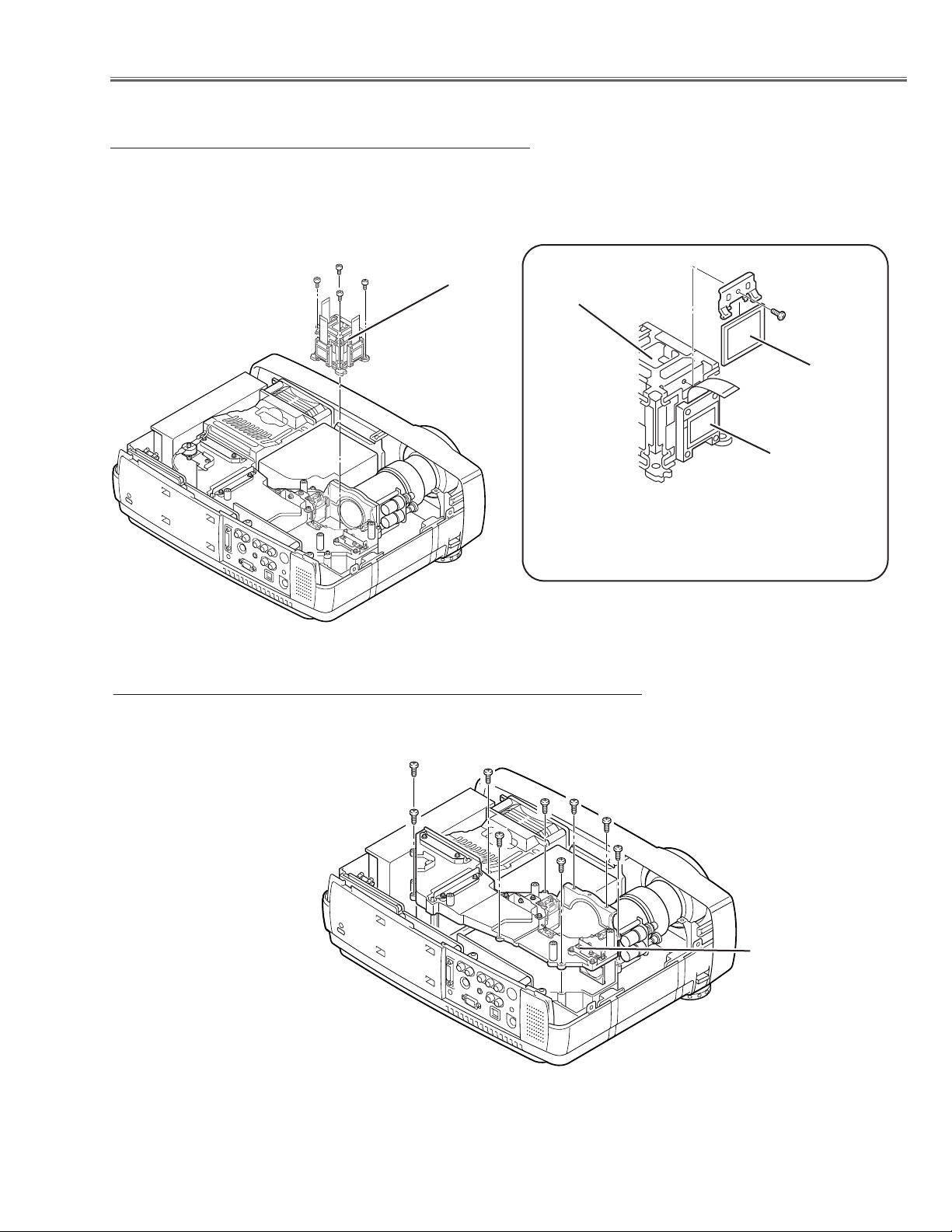
1 Remove 2 screws A and pull the Integrator Lens-In ass’y upward.
2 Remove 1 stoppers B and then take the Lens off from the holder.
Fig.1
■ Optical Parts Disassemblies
Before taking this procedure, remove Cabinet Top and Main Board following to the “Mechanical Disassemblies”.
Disassembly requires a 2.0mm hex wrench and a screwdriver.
Integrator Lens
* Lens should be placed as the
rugged surface side comes to
the holder side.
Fig.2-
1
Fig.2-2
Projection Lens removal
Integrator Lens-In disassembly
Stopper B
A
A
Page 15
-15-
1 Remove 2 screws A and pull the Condenser Lens ass’y upward.
2 Remove 4 screws B to take the Lens off from the holder.
1 Remove 2 screws A and pull the Condenser Lens-Out ass’y upward.
2 Remove 2 screws B to take the Lens off from the holder.
Note:
Should be place the lens as shown in the figure.
A
Optical Pats Disassemblies
B
Condenser Lens
Fig.3-2
Fig.3-1
* Lens should be placed as the flat
surface side comes to the holder
side.
Holder
A
A
Fig.4-2
Fig.4-1
B
B
Holder
Condenser Lens-Out
A
Condenser lens disassembly
Condenser Lens-Out disassembly
B
B
B
Side View
Page 16
-16-
Optical Parts Disassemblies
1 Remove 2 screws A and pull the Relay Lens-Out ass’y upward.
2 Remove 2 screws B to take the Lens off from the holder.
Note:
There is no mounting direction of the lens.
1 Remove each screw and pull the Polarized Glass-In ass’y upward.
2 Unhook the stoppers and take the glass off upward.
Hooks
Polarized Glass-In
Fig.6-2
Fig.6-1
* Glass should be placed as the
film attached side comes to the
prism side.
Phase Sheet
A
Fig.5-2
Fig.5-1
B
B
Holder
Relay Lens-Out
A
Relay Lens-Out disassembly
Polarized Glass-In removal
Page 17
-17-
1 Remove 4 screws A and take the LCD/Prism ass’y off
upward from the optical unit.
2 Remove each screw B and take the glass off upward.
LCD Panel/
Prism Ass’y
Note:
Do not replace the LCD panel
separately otherwise it can
not obtain proper picture.
1 Remove 9 screws to take the Optical Unit Top off upward.
Fig.7-1
Fig.8
Polarized Glass-Out/Pre-Polarized Glass
removal
Optical Unit Top removal
Optical Parts Disassemblies
A
A
A
Optical Unit Top
Polarized
Glass-Out
LCD Panel/Prism
Ass’y
Fig.7-
2
* Glasses should be placed as the
film attached side comes to the
LCD panel side.
LCD Panel
B
Page 18
-18-
Optical Parts Disassemblies
When mounting or assembling the optical parts in the optical unit, the
parts must be mounted in the specified location and direction as
shown in figure below.
5
8
9
Fig.9
2
4
1
The printed marker
comes this side.
13
3
7
10
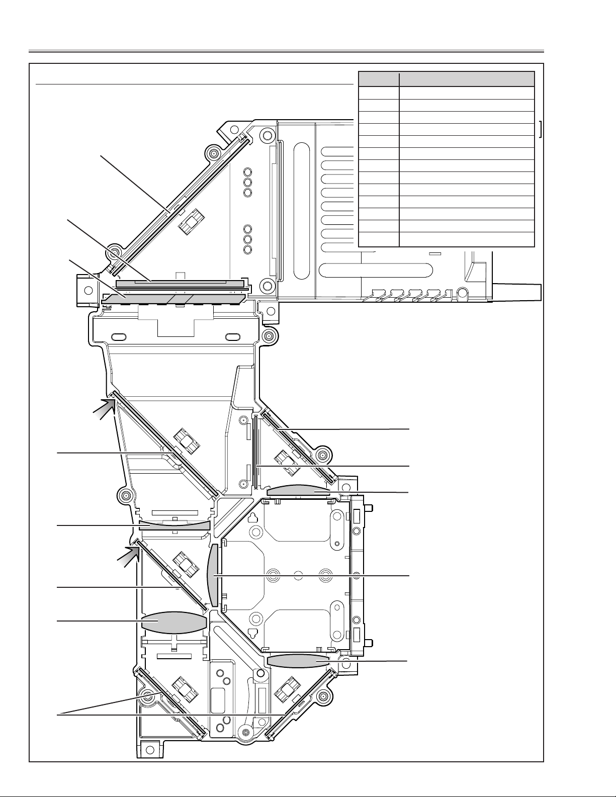
Locations and Directions
6
12
1 Mirror (W)
2 Integrator lens (OUT)
3 Prism beam splitter (PBS)
4 Dichroic mirror (B)
5 Condenser lens (OUT)
6 Dichroic mirror (G)
7 Relay lens (IN)
8 Mirror (R)
9 Condenser lens (R)
10 Condenser lens
11 Condenser lens (B)
12 Optical filter (UV cut)
13 Mirror (B)
Key No. Description
The printed marker
comes this side.
11
Page 19
-19-
■ LCD Panel/Prism Ass’y Replacement
1 Remove the cabinet top and main board following to
“Mechanical Disassemblies”.
2 Remove 4 screws by using the 2.0 mm hex driver and
take the LCD Panel/Prism ass’y off upward from the
optical unit.
LCD Panel/Prism
Ass’y
After replacing or installing the LCD Panel/Prism ass'y,
please make sure to obtain the best focus in both TELE
and WIDE zoom. If the focus adjustment is required,
please adjust the positioning of LCD Panel/Prism Ass’y by
following below procedure.
Mounting Procedure:
1 Loosen 4 screws A on the LCD Panel/Prism ass'y with
2.0 mm hex driver.
2 Turn the projector on and project the image with WIDE
zoom, and adjust the FOCUS control to obtain the best
focus.
3 Turn the ZOOM control to the TELE position.
4 Move the LCD Panel/Prism Ass’y backward or forward
(about 0mm ~ 0.8mm) to obtain the proper focus.
Confirm the focus at TELE and WIDE zoom.
5 Tighten 4 screws A to fix the LCD Panel/Prism ass'y.
T
op View
A
A
A
A
LCD Panel/Prism Ass’y
Note:
Do not replace the LCD
panel separately otherwise
it can not obtain proper picture.
IMPORTANT NOTICE on LCD Panel/Prism Ass'y Replacement
LCD panels used for this model can not be replaced separately. Do not disassemble the LCD Panel/Prism Ass’y.
These LCD panels are installed with precision at the factory. When replacing the LCD panel, should be replaced
whole of the LCD panels and prism ass’y at once.
After replacing LCD Panel/Prism ass’y, please check the following adjustments.
- Check the “Condenser Lens Adjustment” , “Condenser Lens-Out Adjustment” and “Relay Lens-Out
Adjustment” following to chapter “Optical Adjustment”.
- Check the “White Balance Adjustment” , “Common Center Adjustment” and “Gamma Shift Adjustment”
following to chapter “Electrical Adjustment”.
- Check the white uniformity on the screen.
If you find the color shading, please adjust the white uniformity by using the proper computer and
“Color Shading Correction” software supplied separately. The software can be ordered as follows;
COLOR SHADING CORRECTION
Service Parts No. 645 051 2308
LCD Panel/Prism Ass’y removal
Note on LCD Panel/Prism Ass’y Mounting
Page 20
-20-
WARNING:
- For continued safety, replace with a lamp assembly of the same type.
- Allow the projector to cool for at least 45 minutes before you open the
lamp cover. The inside of the projector can become very hot.
- Do not drop the lamp module or touch the glass bulb! The glass can
shatter and cause injury.
Procedure
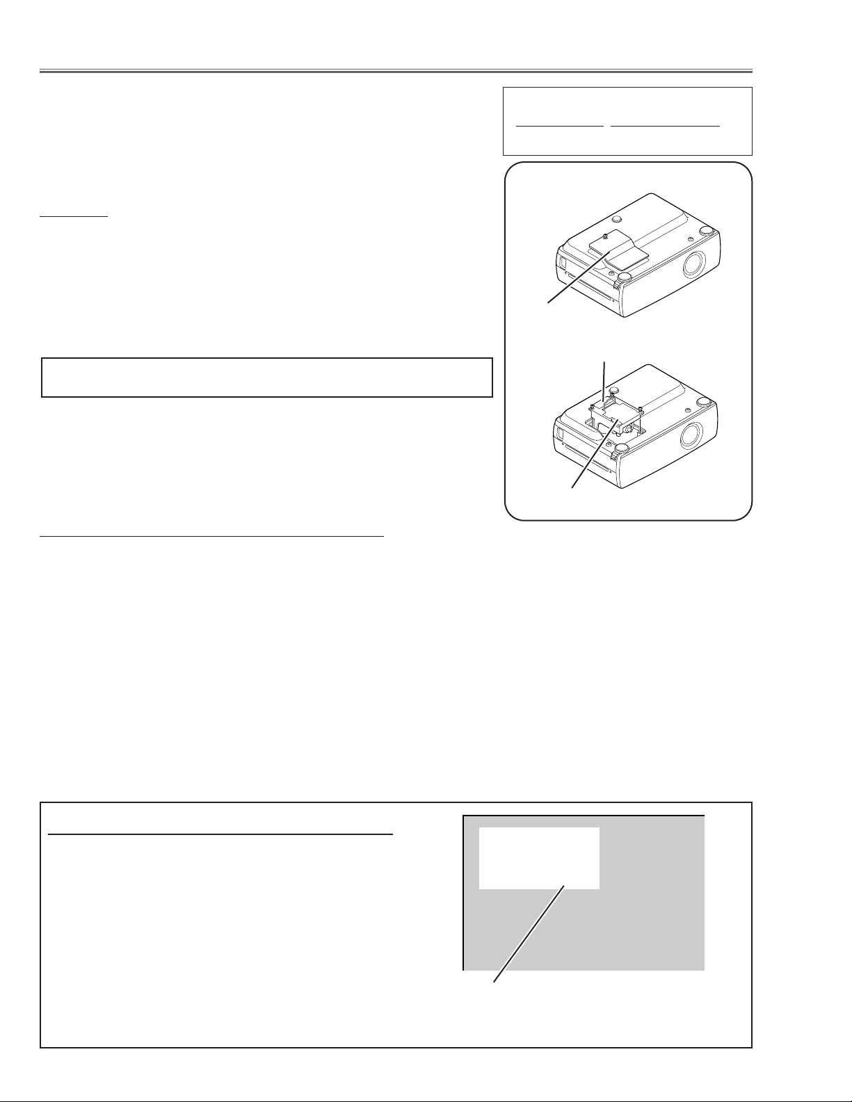
1 Turn off the projector and disconnect the AC cord. Allow the projector to
cool for at least 45 minutes.
2 Remove a screw with a screwdriver and remove the lamp cover.
3 Remove 2 screws and pull out the lamp assembly by grasping the han-
dle.
4 Replace the lamp assembly securely and tighten 3 screws.
5 Place the lamp cover and tighten a screw.
6 Connect the AC cord to the projector and turn on.
Note:
- Do not reset the Lamp Replace Counter, except after lamp is replaced.
- The projector can not be turned-on with lamp cover removed, because
when the lamp cover is removed, the interlock switch is also released to
switch off the mains power for safety.
7 Reset the Lamp Replace Counter, see below explanation.
■ Lamp Replacement
1 Turn the projector on, and press the MENU button
and the on-screen menu will appear. Press the POINT
LEFT/RIGHT buttons to move a red frame pointer to
SETTING menu icon.
2 Press the POINT DOWN button to move a red frame
pointer to “Lamp counter reset” and then press the
SELECT button.The message “Lamp replace counter
reset?” is displayed. Move the pointer to [Yes] and the
press the SELECT button.
3 Another confirmation dialog box appears and select
[Yes] to reset Lamp Replace Counter .
Please refer to the owners manual for further information.
Recommendation
Should the air filter become clogged with dust particles,
it will reduce the cooling fan’s effectiveness and may
result in internal heat build up and short lamp life. We
recommend cleaning the air filter after the projection
lamp is replaced.
Refer to “Air Filter Cleaning”.
Lamp cover
Lamp Assembly
Handle
ORDER REPLACEMENT LAMP
T
ype No.
Service Parts No.
POA-LMP35 610 293 2751
How to reset Lamp Replace Counter
The LAMP REPLACEMENT indicator will illuminate
when the Lamp Replace Counter reaches 1500
hours. This is to indicate that lamp replacement is
required.
You can check the lamp replace counter following to
below procedure.
1 Press and hold the pointer UP on the projector for
more than 20 seconds.
2 The Lamp replace Counter is displayed on upper
left corner of the screen briefly.
* This model does not have Eco mode.
Lamp replace counter data
How to check Lamp Replace Counter
Normal 123 h
Eco 0 h
Total 123 h
Page 21
-21-
[Before Adjustment]
- Input a 100% of black raster signal.
[R/G/B-CONTRAST ADJUSTMENT]
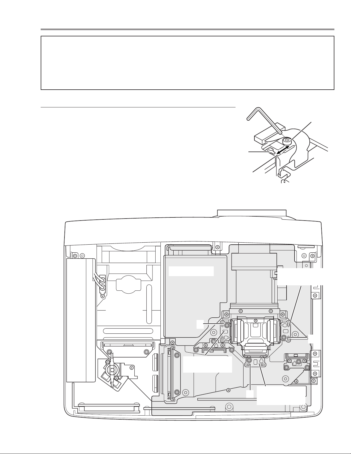
1 Loosen a screw A (Fig.1-1/1-2) on the polarized glass mounting
base which you intend to adjust.
2 Turn the polarized glass mounting base as shown in Fig.1-1 to
obtain the darkest brightness on the screen.
3 Tighten the screw A to fix the polarized glass mounting base.
Repeat steps 1 to 3 for remaining polarized glasses.
B-Polarized Glass
Mounting Base
R-Polarized Glass
Mounting Base
G-Polarized Glass
Mounting Base
A
A
A
Slot B
Fig.1-2
Fig.1-1
Polarized glass
mounting base
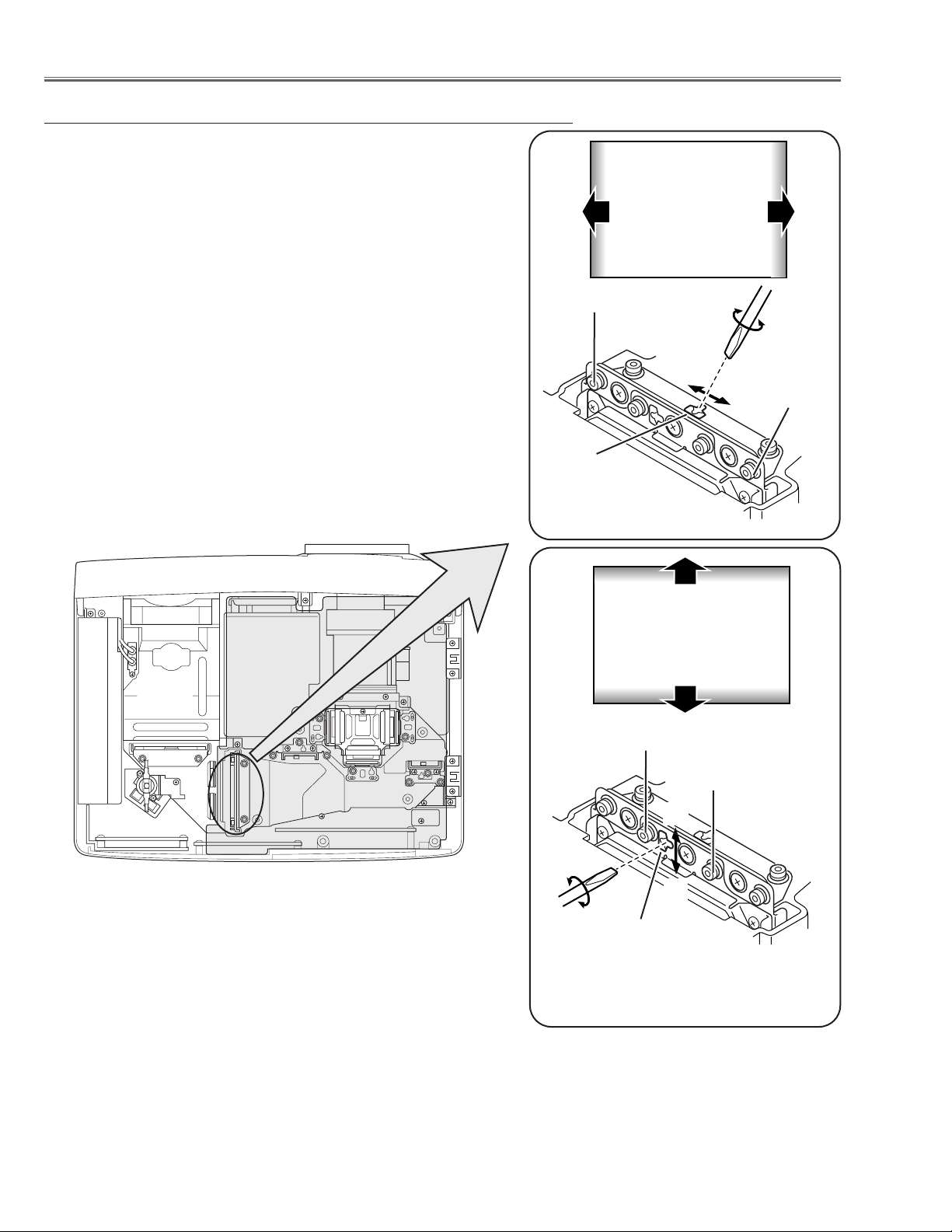
■ Optical Adjustments
Main Board
A
Contrast adjustment
Before taking optical adjustments below, remove the Cabinet Top and Main Board following to the “Mechanical
Disassemblies”
Adjustments require a 2.0mm hex wrench and a slot screwdriver. When you adjust Condenser lens, Condenser
lens-out or Relay lens adjustment, you need to disconnect some connectors and FPC cables of LCD panels on the
main board.
Note: Do not disconnect connectors K8N, K8P, K8H, K8R and K8S on the main board, because the projector can
not turn on due to operate the power failure protection.
Page 22
-22-
Optical Adjustments
Fig.2-2
1 Turn the projector on by a state of without FPC cables.
2 Project only green light on the screen.
3 Adjust the adjustment base of condenser lens assy to make color
uniformity in green.
1) If the shading appears on the left or right of the screen as
shown in Fig.2-1, loosen 2 screws A with the 2.0mm hex driver, and adjust the slot B to make color uniformity in green by
using a slot screwdriver.
2) If the shading appears on the top or bottom of the screen as
shown in Fig.2-2, loosen 2 screw C with the 2.0mm hex driver,
and adjust the slot D to make color uniformity in green by using
a slot screwdriver
4 Tighten screws A and C to fix the Condenser lens unit.
Note:
The relay lens adjustment must be carried out after completing this
adjustment.
y
x
Moving of Slot D
Slot D
C
a
b
a
b
Moving of slot B
Fig.2-1
Slot B
A
C
y
x
Green
Green
Condenser Lens adjustment
A
Page 23
-23-
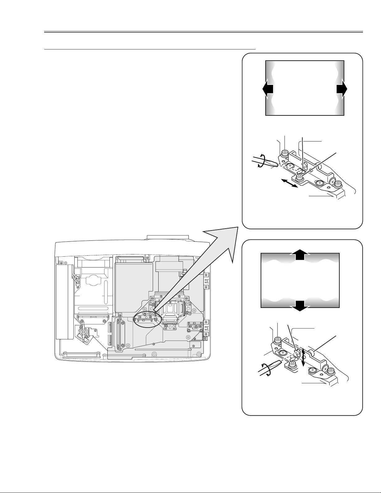
1 Turn the projector on by a state of without FPC cables.
2 Project green and blue lights on the screen.
3 Adjust the adjustment base of condenser lens-out assy to make
color uniformity in cyan.
1) If the shading appears on the left or right of the screen as shown
in Fig.3-1, loosen 1 screw A with the 2.0mm hex driver, and
adjust the slot B to make color uniformity in cyan by using a slot
screwdriver.
2) If the shading appears on the top or bottom of the screen as
shown in Fig.3-2, loosen 1 screw C with the 2.0mm hex driver,
and adjust the slot D to make color uniformity in cyan by using a
slot screw driver.
4 Tighten the screw A and C to fix the relay lens unit.
Fig.3-1
A
Slot B
Optical Adjustments
a
b
b
Moving of slot B
a
Cyan
Fig.3-2
D
Moving of slot D
y
x
C
Condenser Lens-Out adjustment
y
x
Cyan
Page 24
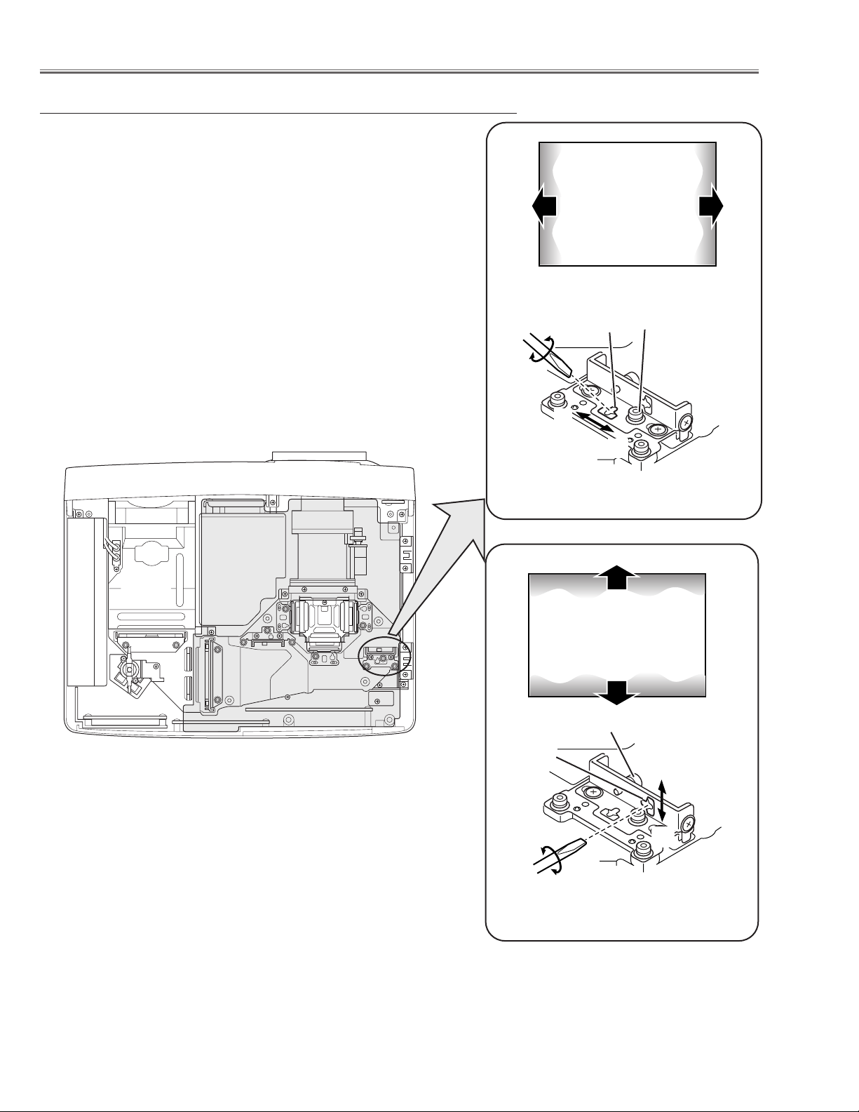
-24-
1 Turn the projector on by a state of without FPC cables.
2 Project all of lights on the screen.
3 Adjust the adjustment base of relay lens assy to make color unifor-
mity in white.
1) If the shading appears on the left or right of the screen as shown
in Fig.4-1, loosen 1 screw A with the 2.0mm hex driver, and
adjust the slot B to make color uniformity in white by using a slot
screwdriver.
2) If the shading appears on the top or bottom of the screen as
shown in Fig.4-2, loosen 1 screw C with the 2.0mm hex driver,
and adjust the slot D to make color uniformity in white by using
a slot screwdriver.
4 Tighten the screws A and C to fix the relay lens unit.
Fig.4-1
A
Slot B
a
b
b
Moving of slot B
a
White
Fig.4-2
Slot D
Moving of slot D
y
x
C
Optical Adjustments
y
x
Relay lens-Out adjustment
White
Page 25
-25-
■ Electrical Adjustments
To enter the service mode
To enter the “Service Mode”, press and hold the MENU and IMAGE button on the projector at the same time for
more than 3 seconds. The service menu appears on the screen as follows.
To adjust service data
Select the adjustment group no. by pressing the MENU (+) or IMAGE (-) button, and select the adjustment item
no. by pressing the pointer UP or DOWN button, and change the data value by pressing the VOLUME – or VOL-
UME + button. Refer to the “Service Adjustment Data Table” for further description of adjustment group no., item
no. and data value.
To exit the service mode
To exit the service mode, press the POWER ON-OFF button on the projector or remote control unit.
● Service Adjustment Menu Operation
IC1801 on the main board stores the data for the service adjustments, and should not be replaced except for
the case of defective device.
If replaced, it should be performed the re-adjustments
following to the “Electrical Adjustments”.
The data of lamp replacement monitor timer is stored
in the IC1801.
Please note that the lamp replace counter is reset
when the memory IC (IC1801) is replaced.
(Lamp replace counter can not be set to the previous
value.)
● Caution to memory IC replacement
When IC1801 is replaced with new one, the CPU
writes down the default data of the service adjustments
to the replaced IC, refer to the service adjustment
table. As these data are not the same data as factory
shipped data, it should be required to perform the re-
adjustments following to the “Electrical Adjustments”.
Please note that the lamp replace counter is reset.
● Caution of Main Board replacement (in the case
IC1801 is not defective)
When the main board is replaced, IC1801 should be
replaced with the one on previous main board. After
replacement, it should be required to perform the readjustments following to the “Electrical Adjustments”.
In this case, the lamp replace counter can be kept the
v
alue as before.
● Memory IC Replacement
Group No.
Data value
Item No.
Service Mode
Input Video
Group No. Data
0032
Ver. 1 .00
Page 26

-26-
After replacing the Power Board, PF.C. Board, readjust
the Output voltage adjustment as follows.
1. Connect a digital voltmeter to pins 1 (+) and 3 (-) of
K6D.
2. Adjust the voltage by using VR611 as following.
A
C Input Reading
230V 370V ±2V
or 120V 340V ±2V
Caution:
Be sure to connect the lamp when taking this adjustment.
● Circuit Adjustments
CAUTION: The each circuit has been made by the fine adjustment at factory. Do not attempt to adjust the follow-
ing adjustments except requiring the readjustments in servicing otherwise it may cause loss of performance and product safety.
[Adjustment Condition]
● Input signal
Video signal .......................... 1.0Vp-p/75Ω terminated, 16 steps gray scale (Composite video signal)
Computer signal...................... 0.7Vp-p/75Ω terminated, 16 steps gray scale pattern (SVGA)
● Picture control mode ...................... “STANDARD” mode unless otherwise noted.
Note:
* Please refer to “Service Adjustment Menu Operation” for entering to the service mode and adjusting the service
data.
Electrical Adjustments
Output Voltage adjustment
1. Enter the service mode and select group no. “11” and
item no. “0”. Set data value to “1”.
2. Connect a digital voltmeter to test point “TP12V1” (+)
and chassis ground (-). Select item no. “1” and change
data value to adjust voltage to be 7.5 ±0.1V.
3. Connect a digital voltmeter to test point “TP12V2” (+)
and chassis ground (-). Select item no. “2” and
change data value to adjust voltage to be 9.0 ±0.1V.
4. Select group no. “11” and item no. “0” and set data
value to “3”.
5. Connect a digital voltmeter to test point “TP12V1” (+)
and chassis ground (-). Select item no. “3” and change
data value to adjust voltage to be 13.5 ±0.1V.
6. Connect a digital voltmeter to test point “TP12V2” (+)
and chassis ground (-). Select item no. “4” and change
data value to adjust voltage to be 13.5 ±0.1V.
Fan Voltage adjustment
Page 27
-27-
Electrical Adjustments
1. Receive the 16-step grey scale computer signal.
2. Set to COMPUTER mode.
3. Enter the service mode.
[R-SIGNAL CENTER ADJUSTMENT]
4. Connect a digital voltmeter to test point “TP25R1” (+)
and chassis ground (-).
5. Select group no. “3”, item no. “0” and change data
value to adjust the voltage to be 7.30 ±0.05V.
[G-SIGNAL CENTER ADJUSTMENT]
6. Connect a digital voltmeter to test point “TP25G1” (+)
and chassis ground (-).
7. Select group no. “3”, item no. “1” and change data
value to adjust the voltage to be 7.30 ±0.05V.
[B-SIGNAL CENTER ADJUSTMENT]
8. Connect a digital voltmeter to test point “TP25B1” (+)
and chassis ground (-).
9. Select group no. “3”, item no. “2” and change data
value to adjust the voltage to be 7.30 ±0.05V.
1. Receive the 16-step grey scale computer signal.
2. Set to COMPUTER mode.
3. Connect an oscilloscope to test point “TP3551” (+)
and chassis ground (-).
4. Enter the service mode, select group no. “3”, item no.
“7” and change data value to adjust amplitude “a” to
be 4.8 ±0.1V.
Signal Center adjustment
NRS adjustment
1. Receive the 16-step grey scale computer signal.
2. Set to COMPUTER mode.
3. Enter the service mode.
[R-BLACK ADJUSTMENT]
4. Connect an oscilloscope to test point “TP25R1” (+)
and chassis ground (-).
5. Select group no. “3”, item no. “3” and change data
value to adjust amplitude “a” to be 10.0 ±0.1V.
[R-BLACK ADJUSTMENT-]
6. Connect an oscilloscope to test point “TP25G1” (+)
and chassis ground (-).
7. Select group no. “3”, item no. “4” and change data
value to adjust amplitude “a” to be 10.0 ±0.1V.
[R-BLACK ADJUSTMENT-]
8. Connect an oscilloscope to test point “TP25B1” (+)
and chassis ground (-).
9. Select group no. “3”, item no. “5” and change data
value to adjust amplitude “a” to be 10.0 ±0.1V.
Black Level adjustment
1. Receive the 16-step grey scale video signal.
2. Set to VIDEO mode.
3. Enter the service mode.
[R-PEDESTAL ADJUSTMENT]
4. Connect an oscilloscope to test point “TP201R” (+)
and chassis ground (-).
5. Select group no. “3”, item no. “14” and change data
value to adjust the pedestal level and black level to be
the same level.
[G-PEDESTAL ADJUSTMENT]
6. Connect an oscilloscope to test point “TP201G” (+)
and chassis ground (-).
7. Select group no. “3”, item no. “15” and change data
value to adjust the pedestal level and black level to be
the same level.
[B-PEDESTAL ADJUSTMENT]
8. Connect an oscilloscope to test point “TP201B” (+)
and chassis ground (-).
9. Select group no. “3”, item no. “16” and change data
value to adjust the pedestal level and black level to be
the same level.
Pedestal adjustment
(a)
Pedestal level = Black level
(a)
black level
(a)
black level
Page 28
-28-
Electrical Adjustments
1. Receive the 16-step gray scale computer signal.
2. Set to COMPUTER mode.
3. Enter the service mode.
[R-GAIN ADJUSTMENT]
4. Connect an oscilloscope to test point “TP25R1” (+)
and chassis ground (-).
5. Select group no. “2”, item no. “3” and change data
value to adjust waveform “a” to be minimum amplitude.
[G-GAIN ADJUSTMENT]
6. Connect an oscilloscope to test point “TP25G1” (+)
and chassis ground (-).
7. Select group no. “2”, item no. “4” and change data
value to adjust waveform “a” to be minimum amplitude.
[B-GAIN ADJUSTMENT]
8. Connect an oscilloscope to test point “TP25B1” (+)
and chassis ground (-).
9. Select group no. “2”, item no. “5” and change data
value to adjust waveform “a” to be minimum amplitude.
PC Gain adjustment
1. Receive the 16-step gray scale computer signal.
2. Set to COMPUTER mode.
3. Enter the service mode.
[R-OFFSET ADJUSTMENT]
4. Connect an oscilloscope to test point “TP25R1” (+)
and chassis ground (-).
5. Select group no. “3”, item no. “11” and change data
value to adjust the waveform “a” (black portion ) to
be maximum amplitude.
[G-OFFSET ADJUSTMENT]
6. Connect an oscilloscope to test point “TP25G1” (+)
and chassis ground (-).
7. Select group no. “3”, item no. “12” and change data
value to adjust the waveform “a” (black portion ) to
be maximum amplitude.
[B-OFFSET ADJUSTMENT]
8. Connect an oscilloscope to test point “TP25B1” (+)
and chassis ground (-).
9. Select group no. “3”, item no. “13” and change data
value to adjust the waveform “a” (black portion ) to
be maximum amplitude.
PC Offset adjustment
Black Level
(a)
White Level
(a)
Page 29
-29-
Electrical Adjustments
[PC-GAMMA OFF ADJUSTMENT]
1. Receive the 16-step gray scale computer signal.
2. Set to COMPUTER mode.
3. Enter the service mode, select group no. “2”, item
no. “6” and change data value to reproduce the proper gray scale picture on the screen.
[AV-GAMMA OFF ADJUSTMENT]
4. Receive the 16-step gray scale video signal.
5. Set to VIDEO mode.
6. Enter the service mode, select group no. “2”, item
no. “6” and change data value to reproduce the proper gray scale picture on the screen.
1. Receive the 1 dot black & white pattern computer signal.
2. Set to COMPUTER mode.
3. Enter the service mode.
[G-COMMON CENTER ADJUSTMENT]
4. Project only green light component to the screen.
5. Select group no. “3”, item no. “8” and change data
value to obtain the minimum flicker on the screen.
[B-COMMON CENTER ADJUSTMENT]
6. Project only blue light component to the screen.
7. Select group no. “3”, item no. “9” and change data
value to obtain the minimum flicker on the screen.
[R-COMMON CENTER ADJUSTMENT]
8. Project only red light component to the screen.
9. Select group no. “3”, item no. “10” and change data
value to obtain the minimum flicker on the screen.
Gamma Shift adjustment
Common Center adjustment
1. Receive the 16-step gray scale video signal.
2. Set to VIDEO mode.
3. Enter the service mode.
[R-GAIN ADJUSTMENT]
4. Connect an oscilloscope to test point “TP25R1” (+)
and chassis ground (-).
5. Select group no. “2”, item no. “3” and change data
value to adjust waveform “a” to be minimum amplitude.
[G-GAIN ADJUSTMENT]
6. Connect an oscilloscope to test point “TP25G1” (+)
and chassis ground (-).
7. Select group no. “2”, item no. “4” and change data
value to adjust waveform “a” to be minimum amplitude.
[B-GAIN ADJUSTMENT]
8. Connect an oscilloscope to test point “TP25B1” (+)
and chassis ground (-).
9. Select group no. “2”, item no. “5” and change data
value to adjust waveform “a” to be minimum amplitude.
AV Gain adjustment
[PC WHITE BALANCE ADJUSTMENT]
1. Receive the 16-step gray scale computer signal.
2. Set to COMPUTER mode.
3. Enter the service mode, select group no. “2”, item no.
“7” (Red) or “8” (Blue), and change data values
respectively to make a proper white balance.
[AV WHITE BALANCE ADJUSTMENT]
4. Receive the 16-step grey scale video signal.
5. Set to VIDEO mode.
6. Enter the service mode, select group no. “2”, item no.
“7” (Red) or “8” (Blue), and change data values
respectively to make a proper white balance.
Confirm that the same white balance is obtained in
video and computer input.
White Balance adjustment
If you find the color shading on the screen, please
adjust the white uniformity by using the proper computer and “Color Shading Correction” software supplied
separately. The software can be ordered as follows;
COLOR SHADING CORRECTION
Service Parts No. 645 051 2308
NOTE ON WHITE UNIFORMITY
ADJUSTMENT
(a)
White Level
Page 30
-30-
Group: 0 TB1274
0 TINT 32 0 ~ 63
1 SHP_EQ 2 0 ~ 3
2 SHP_FO 1 0 ~ 3
NTSC,PAL SECAM,NT4.43 S-Video Y,Cb,Cr
3 SHP_GAIN 8 8 9 9 0 ~ 15
NTSC NT4.43 PAL SECAM
4 Y_OUT_LEVEL 30 30 31 31 0 ~ 63
S-Video NTSC S-Video PAL S-Video SECAM Y,Cb,Cr
30 31 31 31
NTSC NT4.43 PAL SECAM
5 C_OUT_LEVEL 32 32 32 32 0 ~ 63
S-Video NTSC S-Video PAL S-Video SECAM Y,Cb,Cr
32 32 32 32
NTSC PAL SECAM NT4.43 PAL 60
6 Y_DELAY 6 6 3 4 4 0 ~ 15
S-Video NTSC S-Video PAL S-Video SECAM S-Video NT4.43 S-Video PAL60
443 34
7 COL_SYS - -
8 X’TAL - -
9 NOISE_DET - -
10 V_FREQ - - Read only
11 Vert. Std - -
12 CID - -
13 V_SIG - -
NTSC,PAL SECAM,NT4.43 S-Video YCbCr
14 Cinema SHP_GAIN 7 7 8 8 0 ~ 15 For cinema mode
Group: 1 CXA2101
0 PICTURE 30 0 ~ 63
1 BRIGHT 31 0 ~ 63
2 R_DRIVE 31 0 ~ 63
3 G_DRIVE 31 0 ~ 63
4 B_DRIVE 31 0 ~ 63
5 HSEP_SEL 1 0 ~ 1
6 CR_OFFSET1 15kHz: 7 Others: 10 0 ~ 15
7 CB_OFFSET1 15kHz: 7 Others: 10 0 ~ 15
8 BLK_BOTTOM 15 0 ~ 15
NTSC PAL, SECAM 1035i Y,Cb,Cr *1 *1 Y, Cb, Cr and Y, Pb, Pr except 1035i
9 R-Y/R 6 13 6 6 0 ~ 15
10 R-Y/B 5 15 5 5 0 ~ 15
11 G-Y/R 8 8 8 8 0 ~ 15
12 G-Y/B 10 4 10 10 0 ~ 15
13 MAT_OUT 0 0 0 1 0 ~ 3
15kHz 480i, 575i 480p, 575p 1080i, 1035i, 720p
14 SYSTEM 0 1 2 0 ~ 3
15 V_TC 3 3 3 0 ~ 3
16 H_WIDTH 3 2 0 0 ~ 3
17 HS_MASK 0 1 1 0 ~ 1
Video, S-Video 480i, 575i 480p, 575p 1080i, 1035i, 720p
18 CTI_LEVEL 2 2 2 2 0 ~ 3
15kHz 480i, 575i 480p, 575p 1080i, 1035i, 720p
19 SUB_SHP 2 2 2 0 ~ 3
20 SHP_FO 0 2 3 0 ~ 3
21 PRE_OVER 2 2 3 0 ~ 3
22 LTI_LEVEL 0 1 1 0 ~ 3
23 D_PIC 0 0 0 0 ~ 3
24 HUE 31 0 ~ 63 Only adjustable for PAL,SECAM
NTSC PAL,SECAM 525i,480p 625i,575p 1035i Others
25 SUB_COL 5 5 12 12 6 9 0 ~ 15
26 SUB_HUE 7 7 8 7 9 6 0 ~ 15
27 Cinema CTI_LEVEL 2 0 ~ 3 Set this value at Cinema Mode
28 Cinema LTI_LEVEL 0 0 ~ 3 Set this value at Cinema Mode
Electrical Adjustments
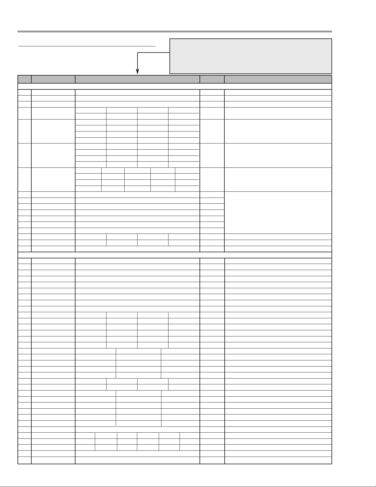
● Service Adjustment Data Table
These initial values are the reference data written from the CPU
ROM to memory IC when replaced new memory IC. The adjustment items indicated with “✻” are required to readjust following
to the “Electrical adjustments”. Other items should be used with
the initial data value.
No. Adjustment Item Initial Value Range Description
Page 31

-31-
Group: 2 L3E07050 (Digital Gamma, Color Shading & Timing Controller)
PC DVI,AV
0 R_SUB_BRT 0 0 0 ~ 1023
1 G_SUB_BRT 0 0 0 ~ 1023
2 B_SUB_BRT 0 0 0 ~ 1023
PC AV DVI
3 R_SUB_GAIN 573 573 492 0 ~ 1023 ✻ Red PC/AV gain adjustment
4 G_SUB_GAIN 573 573 492 0 ~ 1023 ✻ Green PC/AV gain adjustment
5 B_SUB_GAIN 573 573 492 0 ~ 1023 ✻ Blue PC/AV gain adjustment
PC, DVI Standard AV Standard
6 Standard G GAMMA SHIFT 415 415 Note1 ✻ Gamma shift adjustment
7 Standard R GAMMA SHIFT 415 415 Note1 ✻ White balance adjustment
8 Standard B GAMMA SHIFT 415 415 Note1 ✻ White balance adjustment
9 Standard GAMMA 0 0 0 0 ~ 1023
10 Standard GAMMA 1 210 166 0 ~ 1023
11 Standard GAMMA 2 340 290 0 ~ 1023
12 Standard GAMMA 3 436 406 0 ~ 1023
13 Standard GAMMA 4 511 496 0 ~ 1023
14 Standard GAMMA 5 574 560 0 ~ 1023
15 Standard GAMMA 6 633 626 0 ~ 1023
16 Standard GAMMA 7 674 672 0 ~ 1023
17 Standard GAMMA 8 709 709 0 ~ 1023
18 Standard GAMMA 9 740 740 0 ~ 1023
19 Standard GAMMA 10 770 770 0 ~ 1023
20 Standard GAMMA 11 800 800 0 ~ 1023
21 Standard GAMMA 12 832 838 0 ~ 1023
22 Standard GAMMA 13 884 877 0 ~ 1023
23 Standard GAMMA 14 950 940 0 ~ 1023
24 Standard GAMMA 15 1023 1023 0 ~ 1023
PC, DVI Real AV Cinema (Different value to Standard)
25 Real/Cinema G GAMMA SHIFT 506 507 Note1 Note1:
26
Real/Cinema R GAMMA SHIFT 512 512 Note1
27
Real/Cinema B GAMMA SHIFT 504 504 Note1
28 Real/Cinema GAMMA 0 512 512 0 ~ 1023
29 Real/Cinema GAMMA 1 492 538 0 ~ 1023
30 Real/Cinema GAMMA 2 497 524 0 ~ 1023
31 Real/Cinema GAMMA 3 502 519 0 ~ 1023
32 Real/Cinema GAMMA 4 507 516 0 ~ 1023
33 Real/Cinema GAMMA 5 509 515 0 ~ 1023
34 Real/Cinema GAMMA 6 510 512 0 ~ 1023
35 Real/Cinema GAMMA 7 510 511 0 ~ 1023
36 Real/Cinema GAMMA 8 510 510 0 ~ 1023
37 Real/Cinema GAMMA 9 510 510 0 ~ 1023
38 Real/Cinema GAMMA 10 510 510 0 ~ 1023
39 Real/Cinema GAMMA 11 509 510 0 ~ 1023
40 Real/Cinema GAMMA 12 508 510 0 ~ 1023
41 Real/Cinema GAMMA 13 506 509 0 ~ 1023
42 Real/Cinema GAMMA 14 502 502 0 ~ 1023
43 Real/Cinema GAMMA 15 512 512 0 ~ 1023
44 R 2 127 0 ~ 255 R Correction value of vertical line
45 G 2 127 0 ~ 255 G Correction value of vertical line
46 B 2 127 0 ~ 255 B Correction value of vertical line
47 Red MID2 Level 453 0 ~ 1023
48 Red MID1 Level 500 0 ~ 1023
49 Red MAX Level 576 0 ~ 1023
50 Green MID2 Level 453 0 ~ 1023 Gray scale level adjustment
51 Green MID1 Level 500 0 ~ 1023
52 Green MAX Level 575 0 ~ 1023
53 Blue MID2 Level 418 0 ~ 1023
54 Blue MID1 Level 465 0 ~ 1023
55 Blue MAX Level 541 0 ~ 1023
56 DVI std G GAMMA SHIFT 512 0 ~ 1023
57 DVI std R GAMMA SHIFT 512 0 ~ 1023
58 DVI std B GAMMA SHIFT 512 0 ~ 1023
Group: 3 DAC
0 R_VIDEO_CENTER 113 0 ~ 255 ✻ Red Signal center adjustment
1 G_VIDEO_CENTER 113 0 ~ 255 ✻ Green Signal center adjustment
2 B_VIDEO_CENTER 113 0 ~ 255 ✻ Blue Signal center adjustment
3 REF_R 148 0 ~ 255
✻ Red white-black level adjustment
Electrical Adjustments
No. Adjustment Item Initial Value Range Description
Page 32

-32-
4 REF_G 148 0 ~ 255 ✻ Green white-black level adjustment
5 REF_B 148 0 ~ 255 ✻ Blue white-black level adjustment
6 NRS_B 128 0 ~ 255 ✻ NRS adjustment
7 NRS_A 135 0 ~ 255 ✻ NRS adjustment
8 G_V_COM 140 0 ~ 255 ✻ Green common center adjustment
9 B_V_COM 140 0 ~ 255 ✻ Blue common center adjustment
10 R_V_COM 140 0 ~ 255 ✻ Red common center adjustment
11 R_CLMP 63 0 ~ 255 ✻ Red PC offset adjustment
12 G_CLMP 63 0 ~ 255 ✻ Green PC offset adjustment
13 B_CLMP 63 0 ~ 255 ✻ blue PC offset adjustment
14 R_BLK_DC 76 0 ~ 255 ✻ Red pedestal adjustment
15 G_BLK_DC 76 0 ~ 255 ✻ Green pedestal adjustment
16 B_BLK_DC 76 0 ~ 255 ✻ blue pedestal adjustment
Group: 4 TA1318
15kHz 31kHz 33kHz 45kHz
0 SEP_LEV 0 0 0 0 0 ~ 3
1080i 720p 480p 575i,PAL,SECAM 480i,NTSC
1 HD_PHASE 36 38 36 32 32 0 ~ 63
2 V_FREQ - - Read only
3 H_FREQ - -
4 HD_IN - -
Group: 5 LP05 (Turbo)
0 LP05_R_GAIN 128 0 ~ 255
1 LP05_G_GAIN 128 0 ~ 255
2 LP05_B_GAIN 128 0 ~ 255
3 TURBO_GAIN 19 0 ~ 255
Group: 10 Option
0 Lamp Time Monitor - - Read only
1 RS232C Baudrate 0 0 ~ 1 0: 19200bps 1: 9600bps
2 Shootout Mode 0 0 ~ 2
1:Mode-1(Change when no signal input) 2:Mode-2(Priority of AV) 0: Disable
3 Cooling Time 3 0 ~ 15
Set cooling time period 1:30 sec. 3:90 sec. 15:450 sec. 0:On conti.
4 High-Land SW 0 0 ~ 1 0:Nor mal mode(Normal operation) 1:Highland mode(max speed in normal)
5 V-Sync SW 0 0 ~ 1 0:Vertical-synchronized 1:No vertical-synchronized
6 Color Shading SW 1 0 ~ 1
Color correction 0: No 1:Yes, adjustable but does no store the value
7 MCI Output Auto 1 0 ~ 1 Auto: 1, Fixed: 0
8 Keystone Option 0 0 ~ 1 Fixed limitation : 0, Change limitation to the input:1
9 Syukka SW 0 0 ~ 10 Reset the all of user control data to the factory ship data when data changes to 10.
Group: 11 Fan Control ✻ Fan voltage adjustment
0 Fan Speed Mode 0 0 ~ 3 0: Fan control 1:Min., 2: Mid., 3: Max. it can not be memorized.
1 Fan-1 Min Data 44 0 ~ 127 Minimum output data when controlling Fans ✻
2 Fan-2 Min Data 63 0 ~ 127 Minimum output data when controlling Fans ✻
3 Fan-1 Max Data 217 128 ~ 255 Maximum output data when controlling Fans ✻
4 Fan-2 Max Data 236 128 ~ 255 Maximum output data when controlling Fans ✻
5 Temp Low 37 10 ~ 80 Decides output data of DAC for temperature
6 Temp High 45 30 ~ 80 Decides output data of DAC for temperature
7 Fan-1 Temp Error 61 30 ~ 80 Temperature which CPU judges the abnormal temperature
(optical unit temperature, on Main board)
8 Fan-2 Temp Error 51 30 ~ 80 Temperature which CPU judges the abnormal temperature
(outside temperature, on Temp board)
9 Fan-1 Speed Monitor - 0 ~ 255 Read only, displays DAC output data
10 Fan-2 Speed Monitor - 0 ~ 255 Read only, displays DAC output data
11 Temp Monitor - 0 ~ 9999 Read only ( Upper 2 byte indicates for Fan-1.
Lower 2 byte indicates Fan-2)
12 Eco mode Fan-1 Min Data 44 0 ~ 127 decides minimum output data at Eco mode.
13 Eco mode Fan-2 Min Data 63 0 ~ 127 decides minimum output data at Eco mode.
14
Eco mode Fan-1 Max Data 217 128 ~ 255 decides maximum output data at Eco mode.
15 Eco mode Fan-2 Max Data 236 128 ~ 255 decides maximum output data at Eco mode.
Group: 12 PC Real / AV Cinema
0 PC Real Contrast 32 0 ~ 63
1 PC Real Brightness 32 0 ~ 63
2 PC Real Red 32 0 ~ 63
3 PC Real Green 32 0 ~ 63
4 PC Real Blue 32 0 ~ 63
5 PC Real Gamma 8 0 ~ 15
6 AV Cinema Contrast 32 0 ~ 63
7 AV Cinema Brightness 32 0 ~ 63
8 AV Cinema Color 32 0 ~ 63
9 AV Cinema Tint 32 0 ~ 63
10 AV Cinema Red 32 0 ~ 63
Electrical Adjustments
No. Adjustment Item Initial Value Range Description
Page 33

-33-
11 AV Cinema Green 32 0 ~ 63
12 AV Cinema Blue 32 0 ~ 63
13 AV Cinema Sharpness 15 0 ~ 31
14 AV Cinema Gamma 8 0 ~ 15
Group: 500 ADC
0 ADC R-OFFSET 128 0 ~ 255
1 ADC G-OFFSET 128 0 ~ 255
2 ADC B-OFFSET 128 0 ~ 255
3 ADC R-GAIN 254 0 ~ 255
4 ADC G-GAIN 254 0 ~ 255
5 ADC B-GAIN 254 0 ~ 255
6 ADC BandWidth PC 3 0 ~ 3
7 ADC BandWidth AV 3 0 ~ 3
Group: 510 NTSC Gakaku
0 NTSC TOTAL DOTS 2054 0 ~ 2047
1 NTSC DISP DOTS 800 0 ~ 2047
2 NTSC H BACK PORCH 180 0 ~ 2047
3 NTSC V BACK PORCH 46 0 ~ 2047
4 NTSC DISP LINE 456 0 ~ 2047
5 NTSC CLAMP 4 0 ~ 2047
Group: 511 PAL Gakaku
0 PAL TOTAL DOTS 2102 0 ~ 2047
1 PAL DISP DOTS 800 0 ~ 2047
2 PAL H BACK PORCH 207 0 ~ 2047
3 PAL V BACK PORCH 62 0 ~ 2047
4 PAL DISP LINE 533 0 ~ 2047
5 PAL CLAMP 4 0 ~ 2047
Group: 512 HDTV 1080i-60 Gakaku
0 TOTAL DOTS 942 0 ~ 2047
1 DISP DOTS 800 0 ~ 2047
2 H BACK PORCH 115 0 ~ 2047
3 V BACK PORCH 52 0 ~ 2047
4 DISP LINE 1048 0 ~ 2047
5 CLAMP 5 0 ~ 2047
Group: 513 HDTV 1080i-50 Gakaku
0 TOTAL DOTS 1130 0 ~ 2047
1 DISP DOTS 800 0 ~ 2047
2 H BACK PORCH 113 0 ~ 2047
3 V BACK PORCH 64 0 ~ 2047
4 DISP LINE 1044 0 ~ 2047
5 CLAMP 5 0 ~ 2047
Group: 514 HDTV 1035i Gakaku
0 TOTAL DOTS 942 0 ~ 2047
1 DISP DOTS 800 0 ~ 2047
2 H BACK PORCH 115 0 ~ 2047
3 V BACK PORCH 90 0 ~ 2047
4 DISP LINE 1006 0 ~ 2047
5 CLAMP 5 0 ~ 2047
Group: 515 HDTV 720p Gakaku
0 TOTAL DOTS 1060 0 ~ 2047
1 DISP DOTS 800 0 ~ 2047
2 H BACK PORCH 206 0 ~ 2047
3 V BACK PORCH 36 0 ~ 2047
4 DISP LINE 698 0 ~ 2047
5 CLAMP 5 0 ~ 2047
Group: 516 HDTV 575p Gakaku
0 TOTAL DOTS 1052 0 ~ 2047
1 DISP DOTS 800 0 ~ 2047
2 H BACK PORCH 188 0 ~ 2047
3 V BACK PORCH 60 0 ~ 2047
4 DISP LINE 524 0 ~ 2047
5 CLAMP 0 0 ~ 2047
Group: 517 HDTV 480p Gakaku
0 TOTAL DOTS 1006 0 ~ 2047
1 DISP DOTS 800 0 ~ 2047
2 H BACK PORCH 167 0 ~ 2047
3 V BACK PORCH 46 0 ~ 2047
4 DISP LINE 451 0 ~ 2047
5 CLAMP 0 0 ~ 2047
No. Adjustment Item Initial Value Range Description
Electrical Adjustments
Page 34

-34-
Electrical Adjustments
● MAIN BOARD
Test Points and Locations
TP3551
TP25R1
TP11SC
K25R
TP25R2
TP11SY
TP25G1
TP25G2
TP11CV
K25G
TP11PB
TP11PR
TP62V
IC4101
TP25B1
TP62H
K25B
TP52R
TP201G
TP25B2
TP52G
TP52B
TP201B
TP201R
TP205
IC301
TP12V2
TP12V1
TPDCLK
TPDVS
TPDHS
TP3581
IC401
IC801
K8P
Page 35

-35-
■ Troubleshooting
No Power
The possible causes of No Power are listed below. Please
check following and refer to power supply and protection circuits diagram in the figure opposite.
1. Stop the operation of power supply circuit due
to detection of abnormality
.
- Detected the abnormality on the secondary power supply
lines.
Power failure detection diodes detect an abnormal voltage on the power supply. Check the shortage of secondary circuits, ICs, condensers, etc.
- Detected the operation stop of cooling fans.
Power failure detection diodes detect the fan operation
stop. Check Fans FN901, FN902, FN903, FN904, FN905
and FN906
Check fan's power supply lines and detection diodes and
transistors D69A, D69B, D69C and Q69A
- Detected the abnormal temperature rise inside the projec-
tor.
Temperature sensor ICs detect abnormal temperature.
Check peripheral circuits and sensor ICs IC4881 and
IC2881.
Thermal switch (TSW611) detects abnormal temperature.
Check peripheral circuits and TSW611.
TSW611.................... open in normal
TSW611 shorts when the peripheral temperature is over
90°C.
Thermal switch (SW902) detects abnormal temperature.
Check peripheral circuits and SW902.
SW902...................... short in normal
SW902 opens when peripheral temperature is over
100°C.
- Detected the abnormality on the lamp ballast unit.
The lamp ballast unit outputs error signal (LAMP_ERR)
to pin 47 of IC801.
LAMP_ERR .............. High in abnormal
- Detected the over load/over voltage on power supply circuit.
Feedback circuits detect over load or over voltages.
Check PC641, PC642 and peripheral circuits.
- Operated the mechanical protect on the Interlock switch
(SW904). Check lamp cover fixed correctly.
- Fuse (F601) open.
2. Abnormality occurs on drive signals for power
or lamp circuit.
- Abnormality on power starter signals (POWER, 5V_SW).
POWER signal is output from pin 1 of IC801 and sent to
pin 17 of IC1881, and output from pin 3 by the name of
5V_SW signal. 5V_SW signal drives 15.5V and 9VMCI
power supply circuits on the power board.
POWER/5V_SW ............ High in power on
Check POWER and 5V_SW signals, 9V regulator circuit
Q65A, Q65B, Q65C, IC65A and peripheral circuit, 15.5V
switch circuit Q661, Q662 and peripheral circuit on the
Power Board.
- Abnormality on lamp ballast drive signal (BALLAST_AC).
BALLAST_AC signal is output from pin 39 of IC801 and
sent to pin 11 of IC1881, and output from pin 9 by the
name of BALLAST_AC1 signal. BALLAST_SW1 signal
drives the lamp ballast unit.
Check BALLAST_AC and BALLAST_AC1 signals and
lamp ballast unit.
- Abnormality on fan drive signal (FAN DRIVE).
FAN DRIVE signal is output from pin 41 of IC801 and
sent to pin 15 of IC1881, and output from pin 5 by the
name of FAN DRIVE1 signal. FAN DRIVE1 signal drives
fan supply voltages (12V/12V1) on the power board.
FAN DRIVE/
FAN DRIVE1 .............. High in power on
Check FAN DRIVE/FAN DRIVE1 signals, 12V regulator
circuits IC681, Q681, Q682, Q66A, IC671, Q671, Q672
and peripheral circuits.
- Abnormality on power drive signal (LAMP_BST_SW).
LAMP_BST_SW signal is output from pin 82 of IC801
and sent to pin 2 of IC1871, and output from pin 18 by
the name of LAMP_BST_SW1 signal. LAMP_BST_SW1
signal drives the power factor control IC on the P.F. board
through the Power board.
LAMP_BST_SW/
LAMP_BST_SW1 ............ High in power on
Check LAMP_BST_SW and LAMP_BST_SW1 signal,
photo-coupler PC643, transistors Q651, Q641 and
peripheral circuits.
3. Abnormality occurs on the power circuit.
- Abnormality on power primary circuit
Check Line filters, L601, L602, D614, L611, IC631, D632,
etc.
- Abnormality on power secondary circuit
Check D651, D652, D653, IC651, etc.
Page 36

-36-
Troubleshooting
Power supply drive and protection diagrams and locations
SW902
F601
SW904
IC2881
IC4881
AC IN
FN901FN902
FN903
Powe r
Oscillator
Circuit
15.5V
P.F BOARD
K6D
K6E
147
4
1
TSW611
7
K6F
K6S K8S
LAMP_BST_SW1
On: High
K6S K8S
On: High
On: High
37-38
13-14
9-10
15-16
11-12
IC611
P.F.CONTROL
Failure: Low Failure: Low
1
2
1
2
FN904
F601
Fuse
K6J
K6K
K6M
K6L
SW902
Thermal sw.
Fan Control
IC681IC671
Interlock sw.
15.5V
6V
-6V
Q661
SW904
POWER BOARD MAIN BOARD
LAMP BALLAST UNIT
11
CB1
3
3
CB2
1 3
1
K8B
LAMP_BST_SW1
LAMP
LAMP_SW1
BALAST_AC1
5V_SW5V_SW
FAN DRIVE1FAN DRIVE1
3
LAMP_ERR
FN905
FN906
1 2
K8N
K8P
P-FAILP-FAIL
BUFFER
BUFFER
IC1871
18 2
IC1881
12
9
3
LAMP Ass'y
Failure: High
On: High
On: Low
8
11
On: High
17
On: High
15
47 80 81
48
82
3
39
1
415
TEMP. SENS.
3
5
K48E
TEMP. SENSOR
53
K8E
SCL
SDA
TEMP.SENSOR
IC801
SUB CPU
IC4881
1
2
BOARD
IC2881
1
2
Page 37

-37-
The possible causes of No Picture are listed below. Please
check following and refer to video signal processing diagrams in the figure opposite.
1. No picture from Video source
Composite Video Input
Check composite video signal at pins 45 and 46 of K10U
on the AV Board and K3U on the Main Board.
Check Y, C signals at pins 7 and 9 of IC2101.
Check Y, C signals at pins 5 and 7 of IC1101
S-Video Input
Check S-video signals at pins 39, 40 (Y), 41, 42 (C) of
K10U and K3U.
Check Y, C signals at test points TP11SC and TP11SY.
Check Y, C signals at pins 43 and 44 of IC1101.
Component Input
Check component signals at pins 49, 50(Pb), 51, 52 (Pr)
of K10U and K3U.
Check component signals (Y, Pr, Pb) at test points
TP11CV, TP11PB and TP11PR.
All of video signals
Check component signals (Y, Cr, Cb) at pins 21, 22 and
23 of IC1101.
Check component signals (Y, Cr, Cb) at pins 67, 68 and
69 of IC4101.
Check component signals (Y, Pr, Pb) at pins 73, 74 and
75 of IC4101.
Check Sync signals (AV_HSYNC, AV_VSYNC) at pins 4
and 9 of IC1101.
Check Sync signals (AV_HSYNC, AV_VSYNC) at pins 65
and 66 of IC4101.
Check RGB signals at pin 35, 37 and 39 of IC4101.
Check RGB signals at pins 14, 4 and 15 of IC3101.
Check blanking signal at pin 9, 10, 11 of IC3101.
Check RGB signals at pins 1, 3 and 5 of IC5241.
Check Sync signals (AV_HSYNC, AV_VSYNC) at pins 2
and 12 of IC6261.
Check AV/PC switching signal at pin 22 of IC5241 and
pins 10 and 11 of IC6261.
AV : Low, PC : High
2.
No picture from Computer source [Analog]
Check RGB signals at pins 35-36, 37-38 and 39-40 of
K10V on the DVI Board and K3V on the Main Board.
Check Sync signals (IN_H, IN_V) at pins 5-6 and 3-4) of
K10W on the DVI Board and K3W on the Main Board.
Check RGB signals at pins 1, 3 and 5 of IC5211.
Check RGB signals at pins 12, 10 and 8 of IC5241.
Check Sync signals at pins 13 and 11 of IC6241.
Check Sync signals at pins 1 and 13 of IC6261.
Check AV/PC switching signal at pin 22 of IC5241 and
pins 10 and 11 of IC6261.
AV : Low, PC : High
3. No picture fr
om DVI source.
Check power supply voltages on the DVI board.
5VDVI on pins 39-40, 5VS on pins 35-36, 3.3VS on pins
31-32, 9VMCI on pins 35-8, 5VD on pins 21-22 of K10W
and K3Ws.
Check Sync signal at pins 16 and 18 of IC8081.
Check ICs IC8001, IC7021, IC7031 and peripheral circuits.
4. No picture from both of Video and Computer
sources.
Check RGB signals at test points TP52R, TP52G and
TP52B.
Check RGB signals at test points TP201R, TP5201G and
TP201B.
Check HSYNC signal at test point TP205.
Check Sync signals at test points at TP62H and TP62V.
5.
No picture from all of sources
Check RGB S&H signals at test points TP25B1, TP25G1
and TP25R1.
Check NRS signals at test points TP3551 and TP3581.
Check power supply circuit 15.5V and 15VL and peripheral circuit.
Check ICs IC501, IC531, IC561, IC3561, IC801, IC301,
IC401and peripheral circuits.
Troubleshooting
No Picture
SIGNAL K10W/K3W
V-Sync 3-4
H-Sync 5-6
SIGNAL K10V/K3V
B 35-36
G 37-38
R 39-40
SIGNAL K10U/K3U
Video 45-46
S-C 41-42
S-Y 39-40
PB 49-50
PR 51-52
Page 38

-38-
Troubleshooting
Video Signal processing diagrams
10|77
K3V
K10V
DIGITAL/ANALOG
TP25B1
D_RE0-7
D_R00-7
D_GE0-7
D_G00-7
D_BE0-7
D_B00-7
IC8001
80|90
PX+-, CLK, DATA
|
9
DVI
K25B
GHS
GVS
16
18
246
48|46
I/F
DVI
ANALOG SYNC
ANALOG RGB
3|6
40
B-LCD
PAN E L
IC501
S&H_B
B
TP201R
IC8081
BUFFER
TP52R
IC5241
8
AV/PC-RGB-SW
R
IC5211
1
CG1/CG2 RGB-SW
K3W
K10W
MONITOR
DVI BOARD
34
133
R
IC5271
G
3
DBB0-9
7
TP52G
20
12
10
B
20
5
3
|
12
RGB
TP25G1
IC401
GB00-7
15
TP201G
G
IC5281
18
18
15
K25G
DGB0-9
COLOR
DIGITAL
DGB0-9
DGA0-9
IC1401
DIGITAL
DB0-9
DG0-9
GBE0-7
GG00-7
IC201
22
TP201B
B
IC5291
TP52B
16
315
R
G
16
16
H-SYNC
IC531
GGE0-7
19
V-S YN C
G-LCD
PAN E L
IC3531
G_LEVEL
S&H_G
G
TIMING
CONTROL
UNIFORMITY
CORRECTION
DRA0-9
9,1
5,4
CONTROL
BRIGHTER
DR0-9
IC301
SCAN
SYSTEM
CONVERTER
GR00-7
GRE0-7
A/D
40
HSYNC
TP205
IC251
HAFC
16
DET
AFC
IC6171
PC : H
AV : L
22
B
CG1/CG2
22
K3T
20
K10T
TP3551
22
SHIFT
DRB0-9
6,7 13
TPDHS
TPDVS
CONTROL
IC6271
AV/PC
IC5251
2
1
21 22
IC6251
AV/ PC
IC6241
IC6201
NRS
IC3551
6
3
TP25R1
IC561
R
DHS/DVS
TPCLK
244
323
34
V
H
HS
TP62H
TP62V
3
2
BUFFER
15
2
1
SYNC-SW
V
H
12
1
INVERTER
V
H
13
2
3
5
SYNC DET.
8
5
11 9
SYNC SW
VSYNC
HSYNC
K25R
S&H_R
TURBO_1
DCLK
240
133
VS
6
5
14
13
12
8
5
11
16
R-LCD
PAN E L
IC3561
R_LEVEL
10 11
CG1/CG2
22
SHIFT
RGT
DWN
|
14
2
D/A
IC1581
PC : H
AV/ PC
MAIN BOARD
AV BOARD
TP3581
7
3
NRS
IC3581
SUB
D/A
Y
CPU
IC801
79,78
SCL2_5
SDA2_5
I/O
IC2181
2
9,18,19
BLKC_DC
11
C_SWIN
3
12
S_SW
15
13
8
7
4,5,6
7
8
AV/P C
PC : H
AV : L
SYNC_SW
S-In: H
Component-In: H
DIGITAL
2
COMB
FILTER
C_SWIN
7
9
IC2101
CV
353633
34
IC5161
Cb_SW
45
46
Cr_SW
VIDEO/Y
NRS
VCOM
5
7
|
19
3
AV : L
H
IC2571
VIDEO_RGB
V
D/A
12
13
2
3
BLANK_SW
Pr
515249
IC2161
Pb
C
Y
50
IC6101
INVERTER
AV_HSYNC
TP11SC
IC3101
BLANKING
R
55 56
66
6529286968
HD_VSYNC
HD_HSYNC
4
8
12
10
1
5
13
11
AV_VSYNC
9
4
13 14
4344171819
Y/C
TP11SY
TP11PR
K3U
39
41
RGB
IC3121
15
1
3
G
393735
RGB
IC4101
HS_OUT
VS_OUT
Y
VIDEO
IC1101
Cr
Cb
TP11PB
IC2131
IC3141
4
14
9,10
13
2512
B
75
73 74
MATRIX
67
Cr
Cb
212223
7
5
DECODER
CV/Y
TP11CV
K10U
Y/C
S_SW
Pr/Cr
S-VIDEO
Pb/Cb
Page 39

-39-
1. No drive signals supplied at motors
Check drive signals at pins 1 to 4 of K6U on Power Board.
Check ICs IC5501, IC5551 and peripheral circuits. Check
motor drive power supply (9VMCI).
2. No drive signals supplied at motor drive ICs.
Check drive signals at pins 3-4 (ZOOM), 5-6 (FOCUS) of
k6S. Check IC801.
3. No drive signals output from CPU.
Check drive signals at pins 29,30, 33, 34 of IC801(SUB
CPU). Check IC801.
4. No key switch signals input to CPU.
Check signals at pins 50 to 52 of IC801 when pressing the
key buttons. Check key buttons.
Troubleshooting
Logic Table of IC5501/IC5551
Input Output Operation
45 71
H L L H Forward drive
L H H L Reverse drive
H H L L Braking
L L - - Stand by
Lens Motor Problems
No Sound
1. No audio signals at AV input circuit.
Check audio signals at pins14 and 15 of IC5011 on the AV
Board. Check IC5011 and peripheral circuits.
2. Incorrect operation of VIDEO/COMPUTER mode
switching.
Check AV/PC switching signal at pins 10 and 11 of IC5011.
Check IC5011, IC801 and switching signal.
AV : Low, PC : High
3. No audio output signal at speaker.
Check audio signal at pins 1 and 3 of K8F on the Main
Board.
Check MUTE signal at pin 1 of IC001.
Mute On : Low
Check MUTE signal at pin 7 of IC1831, pins 7 and 13 of
IC1881, and peripheral circuit.
Mute On : High
Check sound volume signal at pin 4 of IC001, and pin 14
of IC1831.Check IC IC001, IC1831 and peripheral circuit.
Volume Min.: Low
4. No power suppl
y at audio circuit.
Check 6V(6V AUDIO) power supply line.
AV BOARD MAIN BOARD
COMPUTER
AUDIO IN
VIDEO
AUDIO IN
MONITOR
AUDIO OUT
SPEAKER
PC_L/R
AV_L/R
IC5011
AUDIO-SW
10
11
1
13
15
14
2
12
Q5051
Q5061
Q5072
Q5081
Q5082
AV/PC
Q5031
Q5041
Q011
MUTE
IC001
AUDIO
CONTROL
2
1
MUTE On: H
K3UK10U
PC: H
AV : L
29
30
27
4
28
21
6
|
8
24
MUTE
31
32
K8F
1,3
IC2161
D/A
AV/PC
IC1881
BUFFER
7
7
7
8
VOLUME
13
MUTE On: H
2
3
AUDIO MUTE
IC1831
D/A
14
7
Q1816
Q1817
SCL2_5
SDA2_5
2
SCL1_5
3
SDA1_5
Q1818
Q1819
79,78
80,81
IC801
SUB
CPU
Power
Supply
Circuit
ON: H
5V_SW
4 52
5
4
5
FOCUS
MOTOR
M
ZOOM
MOTOR
M
15V
Q65A
Q65B Q65C
9V MCI
K6U K6S K8S
1
2
3
4
IC5551
FOCUS
MOTOR DRIVE
3
1
7
IC5501
ZOOM
MOTOR DRIVE
3
1
7
POWER BOARD
LEVEL +
IC801
SUB CPU
LEVEL -
345
345
51
50
KEY SW BOARD
IC1881
BUFFER
15
3
16
FOCUS +
6
FOCUS -
5
ZOOM +
4
ZOOM -
3
POWER
ON: H
1
33
34
29
30
17
FOCUS
ZOOM
K68A
K8A
MAIN BOARD
Page 40

-40-
● System Control & I/O Port Table (IC801)
■ Control Port Functions
1 PE5/D5 POWER_SW Power_SW O H: On
2 PE6/D6 SYS SW Peripheral IC power supply SW O L: on
3 PE7/D7 LAMP_SW Lamp LED O H: On
4 PD0/D8 DATA0 Data Bus 0 I/O 5 PD1/D9 DATA1 Data Bus 1 I/O 6 PD2/D10 DATA2 Data Bus 2 I/O 7 PD3/D11 DATA3 Data Bus 3 I/O 8 PD4/D12 DATA4 Data Bus 4 I/O 9 PD5/D13 DATA5 Data Bus 5 I/O -
10 PD6/D14 DATA6 Data Bus 6 I/O -
11 PD7/D15 DATA7 Data Bus 7 I/O 12 CVCC CVCC Power supply - 13 PC0/A0 ADDRESS0 Address Bus 0 O 14 VSS VSS Vss - 15 PC1/A1 ADDRESS1 Address Bus 1 O 16 PC2/A2 ADDRESS2 Address Bus 2 O 17 PC3/A3 ADDRESS3 Address Bus 3 O 18 PC4/A4 ADDRESS4 Address Bus 4 O 19 PC5/A5 ADDRESS5 Address Bus 5 O 20 PC6/A6 ADDRESS6 Address Bus 6 O 21 PC7/A7 ADDRESS7 Address Bus 7 O 22 PB0/A8/TIOCA3 ADDRESS8 Address Bus 8 O 23 PB1/A9/TIOCB3 ADDRESS9 Address Bus 9 O 24 PB2/A10/TIOCC3 ADDRESS10 Address Bus 10 O 25 PB3/A11/TIOCD3 ADDRESS11 Address Bus 11 O 26 PB4/A12/TIOCA4 ADDRESS12 Address Bus 12 O 27 PB5/A13/TIOCB4 ADDRESS13 Address Bus 13 O 28 PB6/A14/TIOCA5 ADDRESS14 Address Bus 14 O 29 PB7/A15/TIOCB5 ZOOM + Zoom + O L: Zoom +
30 PA0/A16 ZOOM - Zoom - O L: Zoom 31 PA1/A17/TxD2 Tx RS232C TxD O L: active
32 PA2/A18/RxD2 Rx RS232C RxD I L: active
33 PA3/A19/SCK2 FOCUS + Focus + O L: Focus +
34 P10/TIOCA0/A20 FOCUS - Focus - O L: Focus 35 P11/TIOCB0/A21 R/C Remote control signal input I L: active
36 P12/TIOCC0/TCLKA/A22 USB_RESET USB Reset signal output O L: active
37 P13/TIOCD0/TCLKB/A23 USB_BRST USB_BRST O L: On”
38 P14/TIOCA1/IRQ0 SCLK Serial clock output O H: active
39 P15/TIOCB1/TCLKC BLAST_AC Lamp Ballast control signal O H: on
40 P16/TIOCA2/IRQ1 TXD_SW TXD_SW O H: PW-Main CPU
41 P17/TIOCB2/TCLKD FAN ON/OFF Fan Drive output O H: on
42 AVSS Avss A/D ground - 43 P97/DA1 PIXEL WRITE PIXEL write I L: PW write
44 P96/DA0 TEMP_DET TEMP DET I L: Temperature abnormal
45 P47/AN7 OPT2 Option input I L: XGA H: SVGA
46 P46/AN6 Not used I
47 P45/AN5 LAMP_ERR Lamp Error I H: Lamp not lit
48 P44/AN4 POWER_FAIL Power Fail (Abnormal less than 2V) I Abnormal less that 1V
49 P43/AN3 OPT1 Destination option I
50 P42/AN2 KEY3 Key Input3 (A/D Input) I
51 P41/AN1 KEY2 Key Input2 (A/D Input) I
52 P40/AN0 KEY1 Key Input1 (A/D Input) I
53 Vref Vref Reference voltage for analog - 54 AVCC AVCC A/D power supply - 55 MD0 MD0 Operation mode control 0 I Fixed L
56 MD1 MD1 Operation mode control 1 I Fixed H
57 OSC2 OSC2 Sub-clock output (Not used) O open
58 OSC1 OSC1 Sub-clock output (Not used) I Connected to GND
59 RES RESET Reset input I Reset L to H
60 NMI NMI Non-maskable input (not used) I Fixed H
61 STBY STBY Stand-by I 62 VCC VCC Vcc - 63 XTAL XTAL Oscillator input I 64 VSS VSS GND - 65 EXTAL EXTAL Oscillator output O 66 FWE FEW Write enable input for Flash ROM I H: Enable
Pin No. Name Function Name Function I/O Action
Page 41

-41-
67 MD2 MD2 Operation mode control 2 I Fixed H
68 PF7/¢ ¢ ¢ output O 69 PF6/AS AS AS output O 70 PF5/RD RD Read signal O Control for SRAM
71 PF4/HWR HWR Write signal (upper 8 bit) O Control for SRAM
72 PF3/LWR/ADTRG/IRQ3 IRO_CS Color uniformity correction (E7050) Chip Select O L: active
73 PF2/WAIT TURBO_CS Turbo gate array Chip Select O H: active
74 PF1/BACK/BUZZ SDA 4 IIC Bus 4 SDA I/O L: active
75 PF0/BREQ/IRQ2 FLASH_MODE FWE control O
76 P30/TxD0 PW TX PW365 TxD O L: active
77 P31/RxD0 PW RX PW365 RxD I L: active
78 P32/SCK0/SDA1/IRQ4 SDA 2 IIC Bus 2 SDA I/O L: active
79 P33/TxD1/SCL1 SCL 2 IIC Bus 2 SCL O L: active
80 P34/RxD1/SDA0 SDA 1 IIC Bus 1 SDA (EEPROM,DAC-1) I/O L: active
81 P35/SCK1/SCL0/IRQ5 SCL 1 IIC Bus 1 SCL (EEPROM,DAC-1) O L: active
82 P36 BLAST_SW Lamp ballast 400VON/OFF O H: on
83 P77/TXD3 MCI TX Viewer TxD O L: active
84 P76/RXD3 MCI RX Viewer RxD I L: active
85 P75/TMO3/SCK3 SCL 4 IIC Bus 4 SCL O L: active
86 P74/TMO2/MRES M-RESET Manual reset I L: reset
87 P73/TMO1/CS7 PW_IN0 PW365 data input 0 I
88 P72/TMO0/CS6 PW_IN1 PW365 data input 1 I
89 P71/TMRI23/TMCI23/CS5 OPT_ECO Eco Mode Option I
90 P70/TMRI01/TMCI01/CS4 OPT_DVI DVI Option I
91 PG0/IRQ6 SDATA Serial data output O L: active
92 PG1/CS3/IRQ7 USB_INTR USB interrupt signal input I L active
93 PG2/CS2 CS 2 SRAM Chip Select O L: active
94 PG3/CS1 CS 1 USB Chip Select O L: active
95 PG4/CS0 CS 0 Not used O Fixed L
96 PE0/D0 SDA 3 IIC Bus 3 SDA I/O L: active
97 PE1/D1 SCL 3 IIC Bus 3 SCL O L: active
98 PE2/D2 PW_OUT0 PW365 Data output 0 O
99 PE3/D3 PW_OUT1 PW365 Data output 1 O
100 PE4/D4 PW_RESET PW365 Reset output O Reset L -> H -> L
Pin No. Name Function Name Function I/O Action
Control Port Functions
Page 42

-42-
1 S Reset Open 2 SCL IIC SCL Active “L” 3 SDA IIC SDA Active “L” 4 D0 CARD_IN L: CARD H: No CARD IN
5 D1 VIEWER_ON L: VIEWER Unit exist IN
6 D2 SCDT1 DVI Sync. detection H: DVI IN
7 D3 TURBO_LED H: on L: off OUT
8 VSS GND - -
9 D4 WARNING_LED H: on L: off OUT
10 D5 LAMPREP_LED H: on L: off OUT
11 D6 READY_LED H: on L: off OUT
12 D7 Not used Fixed “L”OUT
13 VDD 5 V Vcc 14 CS2 Chip Select 2 Fixed “L”15 CS1 Chip Select 1 Fixed “L”16 CS0 Chip Select 0 Fixed “H” -
Pin No. Name Function Action I/O
● IIC Bus I/O Expander (IC1851) Port Functions
● IIC Bus I/O Expander (IC2181) Port Functions
1 R Reset Fixed “H”
2 SCL IIC SCL Active “L”
3 SDA IIC SDA Active “L”
4 AO7 FAN_CONT_1 0xFFh:Min 0x00h:Max
5 AO8 FAN_CONT_2 0xFFh:Min 0x00h:Max
6 AO9 EDIDEN L: H8 side H: PC side
7 AO10 AUDIOMUTE L: Mute Off H: Mute On
8 AO11 PWRDN0 AD Power down (L:DVI/MCI H:PC)
9 AO12 DCOM_OFF Digital Comb Filter Usage L: at composite SECAM, NTSC4.43, PAL60
10 VrefL D/A converter lower ref. voltage Connect to GND
11 VrefU1 D/A converter upper ref. voltage (CH7~CH12) Vcc
12 GND GND GND
13 VrefU2 D/A converter upper ref. voltage (CH1~CH6) Vcc
14 AO1 VOL_CNT Control sound output volume, L: minimum
15 AO2 CG1_CG2 L: CG1, H: CG2
16 AO3 MOUSE Air mouse On/Off H: On L: Off
17 AO4 MOUSE_RESET Air mouse CPU reset Reset start: H->L->H
18 AO5 TURBO + Turbo motor control (+) L: On
19 AO6 TURBO - Turbo motor control (-) L: On
20 Vcc Digital power supply
21 Vdd Analog power supply
22 CS2 Chip Select 2 Fixed “H”
23 CS1 Chip Select 1 Fixed “H”
24 CS0 Chip Select 0 Fixed “L”
Pin No. Name Function Action
● IIC Bus DA Converter (IC1831) Port Functions
Control Port Functions
1 S Reset Open -
2 SCL IIC SCL Active “L”-
3 SDA IIC SDA Active “L”-
4 D0 MOD 2 Composite NTSC4.43, PAL60: H else: L OUT
5 D1 MOD 1 Fixed “L”OUT
6 D2 PNR NTSC, NTSC4.43: L else: H OUT
7 D3 NTPL 2 PAL-M, PAL-N: H else: L OUT
8 VSS GND - -
9 D4 NTPL 1 PAL, PAL-N: H else: L IN
10 D5 4.43 TRAP Composite SECAM, NTSC4.43, PAL60: L, else: H OUT
11 D6 C -SWIN Component signal detection (L: Component) IN
12 D7 S _ SW S signal detection (L: S-Input) IN
13 VDD 5 V Vcc(5V) 14 CS2 Chip Select 2 Fixed “L”15 CS1 Chip Select 1 Fixed “L”16 CS0 Chip Select 0 Fixed “L”-
Pin No. Name Function Action I/O
Page 43

-43-
1 R Reset Fixed “H”
2 SCL IIC SCL Active “L”
3 SDA IIC SDA Active “L”
4 AO7 RCLP R Signal clamp reference voltage
5 AO8 GCLP G Signal clamp reference voltage
6 AO9 BCLP B Signal clamp reference voltage
7 AO10 AV/PC AV/PC switch (L: AV H: PC)
8 AO11 SYNC_SW Fixed “H”
9 AO12 G_BLK_DC Video G signal pedestal voltage
10 VrefL D/A converter lower ref. voltage Connected to GND
11 VrefU1 D/A converter upper ref. voltage (CH7~CH12) Vcc(5V)
12 GND GND GND
13 VrefU2 D/A converter upper ref. voltage(CH1~CH6) Vcc(5V)
14 AO1 SCP SW Sandcastle pulse SW Video/S-Video/480i/575i: L else: H
15 AO2 BLANK SW H Blank width SW 1080i/1035i/720p/480p/575p: H else: L
16 AO3 MACRO H: PC, AV(1080i50Hz) L: AV
17 AO4 CBAL_SW Color uniformity correction SW
18 AO5 B_BLK_DC Video B signal pedestal voltage
19 Ao6 R_BLK_DC Video R signal pedestal voltage
20 Vcc Digital power supply Vcc(5V)
21 Vdd Analo gpower supply Vcc(5V)
22 CS2 Chip Select 2 Fixed “L”
23 CS1 Chip Select 1 Fixed “H”
24 CS0 Chip Select 0 Fixed “H”
Pin No. Name Function Action
● IIC Bus DA Converter (IC2161) Port Functions
Control Port Functions
1 R Reset Fixed “H”
2 SCL IIC SCL Active “L”
3 SDA IIC SDA Active “L”
4 AO7 REF_B D/A reference voltage
5 AO8 REF_G D/A reference voltage
6 AO9 REF_R D/A reference voltage
7 AO10 Not used 0V fixed
8 AO11 Not used 0V fixed
9 AO12 Not used 0V fixed
10 VrefL D/A converter lower ref. voltage Connected to GND
11 VrefU1 D/A converter upper ref. voltage (CH7~CH12) Vcc(5V)
12 GND GND GND
13 VrefU2 D/A converter upper ref. voltage (CH1~CH6) Vcc(5V)
14 AO1 B-CENT Video center voltage
15 AO2 G-CENT Video center voltage
16 AO3 R-CENT Video center voltage
17 AO4 DWN Panel control signal
18 AO5 RGT Panel control signal
19 AO6 XRGT Panel control signal
20 Vcc Digital power supply Vcc(5V)
21 Vdd Analog power supply Vcc(5V)
22 CS2 Chip Select 2 Fixed “L”
23 CS1 Chip Select 1 Fixed “L”
24 CS0 Chip Select 0 Fixed “L”
Pin No. Name Function Action
● IIC Bus DA Converter (IC1581) Port Functions
1 R Reset Fixed “H”
2 SCL IIC SCL Active “L”
3 SDA IIC SDA Active “L”
4 AO5 Not used
5 AO6 VCOMR
6 AO7 VCOMG
7 AO8 VCOMB
8 VrefL D/A converter lower ref. voltage Connected to GND
9 VrefU1 D/A converter upper ref. voltage (CH5~CH8) Connected to Vcc
10 GND GND GND
11 VrefU2 D/A converter upper ref. voltage (CH1~CH4) Connected to Vcc
12 AO1 NRSB
13 AO2 NRSA
14 AO3 Not used
15 AO4 Not used
16 Vcc 5 V Vcc(5V)
17 Vdd 5 V Vdd(5V)
18 CS2 Chip Select 2 Fixed “L”
19 CS1 Chip Select 1 Fixed “L”
20 CS0 Chip Select 0 Fixed “H”
Pin No. Name Function Action
● IIC Bus DA Converter (IC2571) Port Functions
Page 44

-44-
■ Waveforms
VIDEO-IN Y-IN <IC1101-5>
C-IN <IC1101-7>
Y-OUT <IC1101-21> CB-OUT <IC1101-22>
CR-OUT <IC1101-23>
H-SYNC OUT <IC1101-9> V-SYNC OUT <IC1101-4>
R-OUT <IC4101-35> G-OUT <IC4101-37>
B-OUT <IC1101-7>
R-DRIVE <TP52R/TP201R> G-DRIVE <TP52G/TP201G>
B-DRIVE <TP52B/TP201G>
Page 45

H-SYNC OUT <IC4101-29> V-SYNC OUT <IC4101-28>
H-SYNC IN <TP205>
H-SYNC DRIVE <TP62H> V-SYNC DRIVE <TP62V>
DHS <TPDHS>
DVS <TPDVS> NRS <TP3551/TP3581>
R-S&H OUT <TP25R1/TP25R2> G-S&H OUT <TP25G1/TP25G2>
B-S&H OUT <TP25B1/TP25B2>
BALLAST SW <TP28L>
Waveforms
-45-
Page 46

-46-
■ Cleaning
Cleaning with air spray
1. Remove the cabinet top following to “Mechanical
Disassemblies”.
2. Clean up the LCD panel and polarizing plate by using
the air spray from the cabinet top opening.
Caution:
Use a commercial (inert gas) air spray designed for
cleaning camera and computer equipment. Use a resinbased nozzle only. Be vary careful not to damage optical parts with the nozzle tip. Never use any kind of
cleanser on the unit. Also, never use abrasive materials
on the unit as this may cause irreparable damage.
After long periods of use, dust and other particles will accumulate on the LCD panel, prism, mirror, polarized glass,
lens, etc., causing the picture to darken or color to blur. If this occurs, clean the inside of optical unit.
Remove dust and other particles using air spray. If dirt cannot be removed by air spray, disassemble and clean
the optical unit.
Disassembly Cleaning
Disassembly cleaning method should only be performed when the unit is considerable dirty and cannot
be sufficiently cleaned by air spraying alone.
Be sure to readjust the optical system after performing disassembly cleaning.
1. Remove the cabinet top and main units following to
“Mechanical Disassemblies”.
2. Remove the optical base top following to “Optical Unit
Disassemblies”. If the LCD panel needs cleaning,
remove the LCD panel unit following to “LCD panel
replacement”.
3. Clean the optical parts with a soft cloth. Clean
extremely dirty areas using a cloth moistened with
alcohol.
Caution:
The surface of the optical components consists of multiple dielectric layers with varying degrees of refraction.
Never use organic solvents (thinner, etc.) or any kind of
cleanser on these components.
Since the LCD panel is equipped with an electronic circuit, never use any liquids (water, etc.) to clean the unit.
Use of liquid may cause the unit to malfunction.
Page 47

-47-
■ IC Block Diagrams
● AD8183ARU, AD8185ARU <Selector, IC5241, IC5211>
● BA6287F <Motor Drive IC5501, IC5551>
Page 48

-48-
● CXA2101AQ <RGB Matrix, IC4101>
IC Block Diagrams
● BA7078AF <Selector, IC6241>
Page 49

-49-
● CXD2064Q <Digital Comb Filter, IC2101>
● L3E01031 <Level Shift, IC3531, IC3561>
IC Block Diagrams
Page 50

-50-
● L3E06070 <D/A-Sample & Hold, IC501, IC531, IC561>
● L3E07050 <Color, Gamma Correction & Timing Controller , IC401>
IC Block Diagrams
Page 51

-51-
● ML60851 <USB I/F, IC9801>
● M62393 <D/A, IC2571>
IC Block Diagrams
Page 52

-52-
● TA1318N <AFC Detector, IC6171>
● TB1274AF <Video Decoder, IC1101>
IC Block Diagrams
Page 53

-53-
● FA7612CA <PWC Controller, IC65A, IC671, IC681>
IC Block Diagrams
● STR-Z2156 <Switching Controller, IC631>
Page 54

-19-
■ LCD Panel/Prism Ass’y Replacement
1 Remove the cabinet top and main board following to
“Mechanical Disassemblies”.
2 Remove 4 screws by using the 2.0 mm hex driver and
take the LCD Panel/Prism ass’y off upward from the
optical unit.
LCD Panel/Prism
Ass’y
After replacing or installing the LCD Panel/Prism ass'y,
please make sure to obtain the best focus in both TELE
and WIDE zoom. If the focus adjustment is required,
please adjust the positioning of LCD Panel/Prism Ass’y by
following below procedure.
Mounting Procedure:
1 Loosen 4 screws A on the LCD Panel/Prism ass'y with
2.0 mm hex driver.
2 Turn the projector on and project the image with WIDE
zoom, and adjust the FOCUS control to obtain the best
focus.
3 Turn the ZOOM control to the TELE position.
4 Move the LCD Panel/Prism Ass’y backward or forward
(about 0mm ~ 0.8mm) to obtain the proper focus.
Confirm the focus at TELE and WIDE zoom.
5 Tighten 4 screws A to fix the LCD Panel/Prism ass'y.
T
op View
A
A
A
A
LCD Panel/Prism Ass’y
Note:
Do not replace the LCD
panel separately otherwise
it can not obtain proper picture.
IMPORTANT NOTICE on LCD Panel/Prism Ass'y Replacement
LCD panels used for this model can not be replaced separately. Do not disassemble the LCD Panel/Prism Ass’y.
These LCD panels are installed with precision at the factory. When replacing the LCD panel, should be replaced
whole of the LCD panels and prism ass’y at once.
After replacing LCD Panel/Prism ass’y, please check the following adjustments.
- Check the “Condenser Lens Adjustment” , “Condenser Lens-Out Adjustment” and “Relay Lens-Out
Adjustment” following to chapter “Optical Adjustment”.
- Check the “White Balance Adjustment” , “Common Center Adjustment” and “Gamma Shift Adjustment”
following to chapter “Electrical Adjustment”.
- Check the white uniformity on the screen.
If you find the color shading, please adjust the white uniformity by using the proper computer and
“Color Shading Correction” software supplied separately. The software can be ordered as follows;
COLOR SHADING CORRECTION
Service Parts No. 645 051 2308
LCD Panel/Prism Ass’y removal
Note on LCD Panel/Prism Ass’y Mounting
Page 55

-20-
WARNING:
- For continued safety, replace with a lamp assembly of the same type.
- Allow the projector to cool for at least 45 minutes before you open the
lamp cover. The inside of the projector can become very hot.
- Do not drop the lamp module or touch the glass bulb! The glass can
shatter and cause injury.
Procedure
1 Turn off the projector and disconnect the AC cord. Allow the projector to
cool for at least 45 minutes.
2 Remove a screw with a screwdriver and remove the lamp cover.
3 Remove 2 screws and pull out the lamp assembly by grasping the han-
dle.
4 Replace the lamp assembly securely and tighten 3 screws.
5 Place the lamp cover and tighten a screw.
6 Connect the AC cord to the projector and turn on.
Note:
- Do not reset the Lamp Replace Counter, except after lamp is replaced.
- The projector can not be turned-on with lamp cover removed, because
when the lamp cover is removed, the interlock switch is also released to
switch off the mains power for safety.
7 Reset the Lamp Replace Counter, see below explanation.
■ Lamp Replacement
1 Turn the projector on, and press the MENU button
and the on-screen menu will appear. Press the POINT
LEFT/RIGHT buttons to move a red frame pointer to
SETTING menu icon.
2 Press the POINT DOWN button to move a red frame
pointer to “Lamp counter reset” and then press the
SELECT button.The message “Lamp replace counter
reset?” is displayed. Move the pointer to [Yes] and the
press the SELECT button.
3 Another confirmation dialog box appears and select
[Yes] to reset Lamp Replace Counter .
Please refer to the owners manual for further information.
Recommendation
Should the air filter become clogged with dust particles,
it will reduce the cooling fan’s effectiveness and may
result in internal heat build up and short lamp life. We
recommend cleaning the air filter after the projection
lamp is replaced.
Refer to “Air Filter Cleaning”.
Lamp cover
Lamp Assembly
Handle
ORDER REPLACEMENT LAMP
T
ype No.
Service Parts No.
POA-LMP35 610 293 2751
How to reset Lamp Replace Counter
The LAMP REPLACEMENT indicator will illuminate
when the Lamp Replace Counter reaches 1500
hours. This is to indicate that lamp replacement is
required.
You can check the lamp replace counter following to
below procedure.
1 Press and hold the pointer UP on the projector for
more than 20 seconds.
2 The Lamp replace Counter is displayed on upper
left corner of the screen briefly.
* This model does not have Eco mode.
Lamp replace counter data
How to check Lamp Replace Counter
Normal 123 h
Eco 0 h
Total 123 h
Page 56

-21-
[Before Adjustment]
- Input a 100% of black raster signal.
[R/G/B-CONTRAST ADJUSTMENT]
1 Loosen a screw A (Fig.1-1/1-2) on the polarized glass mounting
base which you intend to adjust.
2 Turn the polarized glass mounting base as shown in Fig.1-1 to
obtain the darkest brightness on the screen.
3 Tighten the screw A to fix the polarized glass mounting base.
Repeat steps 1 to 3 for remaining polarized glasses.
B-Polarized Glass
Mounting Base
R-Polarized Glass
Mounting Base
G-Polarized Glass
Mounting Base
A
A
A
Slot B
Fig.1-2
Fig.1-1
Polarized glass
mounting base
■ Optical Adjustments
Main Board
A
Contrast adjustment
Before taking optical adjustments below, remove the Cabinet Top and Main Board following to the “Mechanical
Disassemblies”
Adjustments require a 2.0mm hex wrench and a slot screwdriver. When you adjust Condenser lens, Condenser
lens-out or Relay lens adjustment, you need to disconnect some connectors and FPC cables of LCD panels on the
main board.
Note: Do not disconnect connectors K8N, K8P, K8H, K8R and K8S on the main board, because the projector can
not turn on due to operate the power failure protection.
Page 57

-22-
Optical Adjustments
Fig.2-2
1 Turn the projector on by a state of without FPC cables.
2 Project only green light on the screen.
3 Adjust the adjustment base of condenser lens assy to make color
uniformity in green.
1) If the shading appears on the left or right of the screen as
shown in Fig.2-1, loosen 2 screws A with the 2.0mm hex driver, and adjust the slot B to make color uniformity in green by
using a slot screwdriver.
2) If the shading appears on the top or bottom of the screen as
shown in Fig.2-2, loosen 2 screw C with the 2.0mm hex driver,
and adjust the slot D to make color uniformity in green by using
a slot screwdriver
4 Tighten screws A and C to fix the Condenser lens unit.
Note:
The relay lens adjustment must be carried out after completing this
adjustment.
y
x
Moving of Slot D
Slot D
C
a
b
a
b
Moving of slot B
Fig.2-1
Slot B
A
C
y
x
Green
Green
Condenser Lens adjustment
A
Page 58

-23-
1 Turn the projector on by a state of without FPC cables.
2 Project green and blue lights on the screen.
3 Adjust the adjustment base of condenser lens-out assy to make
color uniformity in cyan.
1) If the shading appears on the left or right of the screen as shown
in Fig.3-1, loosen 1 screw A with the 2.0mm hex driver, and
adjust the slot B to make color uniformity in cyan by using a slot
screwdriver.
2) If the shading appears on the top or bottom of the screen as
shown in Fig.3-2, loosen 1 screw C with the 2.0mm hex driver,
and adjust the slot D to make color uniformity in cyan by using a
slot screw driver.
4 Tighten the screw A and C to fix the relay lens unit.
Fig.3-1
A
Slot B
Optical Adjustments
a
b
b
Moving of slot B
a
Cyan
Fig.3-2
D
Moving of slot D
y
x
C
Condenser Lens-Out adjustment
y
x
Cyan
Page 59

-24-
1 Turn the projector on by a state of without FPC cables.
2 Project all of lights on the screen.
3 Adjust the adjustment base of relay lens assy to make color unifor-
mity in white.
1) If the shading appears on the left or right of the screen as shown
in Fig.4-1, loosen 1 screw A with the 2.0mm hex driver, and
adjust the slot B to make color uniformity in white by using a slot
screwdriver.
2) If the shading appears on the top or bottom of the screen as
shown in Fig.4-2, loosen 1 screw C with the 2.0mm hex driver,
and adjust the slot D to make color uniformity in white by using
a slot screwdriver.
4 Tighten the screws A and C to fix the relay lens unit.
Fig.4-1
A
Slot B
a
b
b
Moving of slot B
a
White
Fig.4-2
Slot D
Moving of slot D
y
x
C
Optical Adjustments
y
x
Relay lens-Out adjustment
White
Page 60

-25-
■ Electrical Adjustments
To enter the service mode
To enter the “Service Mode”, press and hold the MENU and IMAGE button on the projector at the same time for
more than 3 seconds. The service menu appears on the screen as follows.
To adjust service data
Select the adjustment group no. by pressing the MENU (+) or IMAGE (-) button, and select the adjustment item
no. by pressing the pointer UP or DOWN button, and change the data value by pressing the VOLUME – or VOL-
UME + button. Refer to the “Service Adjustment Data Table” for further description of adjustment group no., item
no. and data value.
To exit the service mode
To exit the service mode, press the POWER ON-OFF button on the projector or remote control unit.
● Service Adjustment Menu Operation
IC1801 on the main board stores the data for the service adjustments, and should not be replaced except for
the case of defective device.
If replaced, it should be performed the re-adjustments
following to the “Electrical Adjustments”.
The data of lamp replacement monitor timer is stored
in the IC1801.
Please note that the lamp replace counter is reset
when the memory IC (IC1801) is replaced.
(Lamp replace counter can not be set to the previous
value.)
● Caution to memory IC replacement
When IC1801 is replaced with new one, the CPU
writes down the default data of the service adjustments
to the replaced IC, refer to the service adjustment
table. As these data are not the same data as factory
shipped data, it should be required to perform the re-
adjustments following to the “Electrical Adjustments”.
Please note that the lamp replace counter is reset.
● Caution of Main Board replacement (in the case
IC1801 is not defective)
When the main board is replaced, IC1801 should be
replaced with the one on previous main board. After
replacement, it should be required to perform the readjustments following to the “Electrical Adjustments”.
In this case, the lamp replace counter can be kept the
v
alue as before.
● Memory IC Replacement
Group No.
Data value
Item No.
Service Mode
Input Video
Group No. Data
0032
Ver. 1 .00
Page 61

-26-
After replacing the Power Board, PF.C. Board, readjust
the Output voltage adjustment as follows.
1. Connect a digital voltmeter to pins 1 (+) and 3 (-) of
K6D.
2. Adjust the voltage by using VR611 as following.
A
C Input Reading
230V 370V ±2V
or 120V 340V ±2V
Caution:
Be sure to connect the lamp when taking this adjustment.
● Circuit Adjustments
CAUTION: The each circuit has been made by the fine adjustment at factory. Do not attempt to adjust the follow-
ing adjustments except requiring the readjustments in servicing otherwise it may cause loss of performance and product safety.
[Adjustment Condition]
● Input signal
Video signal .......................... 1.0Vp-p/75Ω terminated, 16 steps gray scale (Composite video signal)
Computer signal...................... 0.7Vp-p/75Ω terminated, 16 steps gray scale pattern (SVGA)
● Picture control mode ...................... “STANDARD” mode unless otherwise noted.
Note:
* Please refer to “Service Adjustment Menu Operation” for entering to the service mode and adjusting the service
data.
Electrical Adjustments
Output Voltage adjustment
1. Enter the service mode and select group no. “11” and
item no. “0”. Set data value to “1”.
2. Connect a digital voltmeter to test point “TP12V1” (+)
and chassis ground (-). Select item no. “1” and change
data value to adjust voltage to be 7.5 ±0.1V.
3. Connect a digital voltmeter to test point “TP12V2” (+)
and chassis ground (-). Select item no. “2” and
change data value to adjust voltage to be 9.0 ±0.1V.
4. Select group no. “11” and item no. “0” and set data
value to “3”.
5. Connect a digital voltmeter to test point “TP12V1” (+)
and chassis ground (-). Select item no. “3” and change
data value to adjust voltage to be 13.5 ±0.1V.
6. Connect a digital voltmeter to test point “TP12V2” (+)
and chassis ground (-). Select item no. “4” and change
data value to adjust voltage to be 13.5 ±0.1V.
Fan Voltage adjustment
Page 62

-27-
Electrical Adjustments
1. Receive the 16-step grey scale computer signal.
2. Set to COMPUTER mode.
3. Enter the service mode.
[R-SIGNAL CENTER ADJUSTMENT]
4. Connect a digital voltmeter to test point “TP25R1” (+)
and chassis ground (-).
5. Select group no. “3”, item no. “0” and change data
value to adjust the voltage to be 7.30 ±0.05V.
[G-SIGNAL CENTER ADJUSTMENT]
6. Connect a digital voltmeter to test point “TP25G1” (+)
and chassis ground (-).
7. Select group no. “3”, item no. “1” and change data
value to adjust the voltage to be 7.30 ±0.05V.
[B-SIGNAL CENTER ADJUSTMENT]
8. Connect a digital voltmeter to test point “TP25B1” (+)
and chassis ground (-).
9. Select group no. “3”, item no. “2” and change data
value to adjust the voltage to be 7.30 ±0.05V.
1. Receive the 16-step grey scale computer signal.
2. Set to COMPUTER mode.
3. Connect an oscilloscope to test point “TP3551” (+)
and chassis ground (-).
4. Enter the service mode, select group no. “3”, item no.
“7” and change data value to adjust amplitude “a” to
be 4.8 ±0.1V.
Signal Center adjustment
NRS adjustment
1. Receive the 16-step grey scale computer signal.
2. Set to COMPUTER mode.
3. Enter the service mode.
[R-BLACK ADJUSTMENT]
4. Connect an oscilloscope to test point “TP25R1” (+)
and chassis ground (-).
5. Select group no. “3”, item no. “3” and change data
value to adjust amplitude “a” to be 10.0 ±0.1V.
[R-BLACK ADJUSTMENT-]
6. Connect an oscilloscope to test point “TP25G1” (+)
and chassis ground (-).
7. Select group no. “3”, item no. “4” and change data
value to adjust amplitude “a” to be 10.0 ±0.1V.
[R-BLACK ADJUSTMENT-]
8. Connect an oscilloscope to test point “TP25B1” (+)
and chassis ground (-).
9. Select group no. “3”, item no. “5” and change data
value to adjust amplitude “a” to be 10.0 ±0.1V.
Black Level adjustment
1. Receive the 16-step grey scale video signal.
2. Set to VIDEO mode.
3. Enter the service mode.
[R-PEDESTAL ADJUSTMENT]
4. Connect an oscilloscope to test point “TP201R” (+)
and chassis ground (-).
5. Select group no. “3”, item no. “14” and change data
value to adjust the pedestal level and black level to be
the same level.
[G-PEDESTAL ADJUSTMENT]
6. Connect an oscilloscope to test point “TP201G” (+)
and chassis ground (-).
7. Select group no. “3”, item no. “15” and change data
value to adjust the pedestal level and black level to be
the same level.
[B-PEDESTAL ADJUSTMENT]
8. Connect an oscilloscope to test point “TP201B” (+)
and chassis ground (-).
9. Select group no. “3”, item no. “16” and change data
value to adjust the pedestal level and black level to be
the same level.
Pedestal adjustment
(a)
Pedestal level = Black level
(a)
black level
(a)
black level
Page 63

-28-
Electrical Adjustments
1. Receive the 16-step gray scale computer signal.
2. Set to COMPUTER mode.
3. Enter the service mode.
[R-GAIN ADJUSTMENT]
4. Connect an oscilloscope to test point “TP25R1” (+)
and chassis ground (-).
5. Select group no. “2”, item no. “3” and change data
value to adjust waveform “a” to be minimum amplitude.
[G-GAIN ADJUSTMENT]
6. Connect an oscilloscope to test point “TP25G1” (+)
and chassis ground (-).
7. Select group no. “2”, item no. “4” and change data
value to adjust waveform “a” to be minimum amplitude.
[B-GAIN ADJUSTMENT]
8. Connect an oscilloscope to test point “TP25B1” (+)
and chassis ground (-).
9. Select group no. “2”, item no. “5” and change data
value to adjust waveform “a” to be minimum amplitude.
PC Gain adjustment
1. Receive the 16-step gray scale computer signal.
2. Set to COMPUTER mode.
3. Enter the service mode.
[R-OFFSET ADJUSTMENT]
4. Connect an oscilloscope to test point “TP25R1” (+)
and chassis ground (-).
5. Select group no. “3”, item no. “11” and change data
value to adjust the waveform “a” (black portion ) to
be maximum amplitude.
[G-OFFSET ADJUSTMENT]
6. Connect an oscilloscope to test point “TP25G1” (+)
and chassis ground (-).
7. Select group no. “3”, item no. “12” and change data
value to adjust the waveform “a” (black portion ) to
be maximum amplitude.
[B-OFFSET ADJUSTMENT]
8. Connect an oscilloscope to test point “TP25B1” (+)
and chassis ground (-).
9. Select group no. “3”, item no. “13” and change data
value to adjust the waveform “a” (black portion ) to
be maximum amplitude.
PC Offset adjustment
Black Level
(a)
White Level
(a)
Page 64

-29-
Electrical Adjustments
[PC-GAMMA OFF ADJUSTMENT]
1. Receive the 16-step gray scale computer signal.
2. Set to COMPUTER mode.
3. Enter the service mode, select group no. “2”, item
no. “6” and change data value to reproduce the proper gray scale picture on the screen.
[AV-GAMMA OFF ADJUSTMENT]
4. Receive the 16-step gray scale video signal.
5. Set to VIDEO mode.
6. Enter the service mode, select group no. “2”, item
no. “6” and change data value to reproduce the proper gray scale picture on the screen.
1. Receive the 1 dot black & white pattern computer signal.
2. Set to COMPUTER mode.
3. Enter the service mode.
[G-COMMON CENTER ADJUSTMENT]
4. Project only green light component to the screen.
5. Select group no. “3”, item no. “8” and change data
value to obtain the minimum flicker on the screen.
[B-COMMON CENTER ADJUSTMENT]
6. Project only blue light component to the screen.
7. Select group no. “3”, item no. “9” and change data
value to obtain the minimum flicker on the screen.
[R-COMMON CENTER ADJUSTMENT]
8. Project only red light component to the screen.
9. Select group no. “3”, item no. “10” and change data
value to obtain the minimum flicker on the screen.
Gamma Shift adjustment
Common Center adjustment
1. Receive the 16-step gray scale video signal.
2. Set to VIDEO mode.
3. Enter the service mode.
[R-GAIN ADJUSTMENT]
4. Connect an oscilloscope to test point “TP25R1” (+)
and chassis ground (-).
5. Select group no. “2”, item no. “3” and change data
value to adjust waveform “a” to be minimum amplitude.
[G-GAIN ADJUSTMENT]
6. Connect an oscilloscope to test point “TP25G1” (+)
and chassis ground (-).
7. Select group no. “2”, item no. “4” and change data
value to adjust waveform “a” to be minimum amplitude.
[B-GAIN ADJUSTMENT]
8. Connect an oscilloscope to test point “TP25B1” (+)
and chassis ground (-).
9. Select group no. “2”, item no. “5” and change data
value to adjust waveform “a” to be minimum amplitude.
AV Gain adjustment
[PC WHITE BALANCE ADJUSTMENT]
1. Receive the 16-step gray scale computer signal.
2. Set to COMPUTER mode.
3. Enter the service mode, select group no. “2”, item no.
“7” (Red) or “8” (Blue), and change data values
respectively to make a proper white balance.
[AV WHITE BALANCE ADJUSTMENT]
4. Receive the 16-step grey scale video signal.
5. Set to VIDEO mode.
6. Enter the service mode, select group no. “2”, item no.
“7” (Red) or “8” (Blue), and change data values
respectively to make a proper white balance.
Confirm that the same white balance is obtained in
video and computer input.
White Balance adjustment
If you find the color shading on the screen, please
adjust the white uniformity by using the proper computer and “Color Shading Correction” software supplied
separately. The software can be ordered as follows;
COLOR SHADING CORRECTION
Service Parts No. 645 051 2308
NOTE ON WHITE UNIFORMITY
ADJUSTMENT
(a)
White Level
Page 65

-30-
Group: 0 TB1274
0 TINT 32 0 ~ 63
1 SHP_EQ 2 0 ~ 3
2 SHP_FO 1 0 ~ 3
NTSC,PAL SECAM,NT4.43 S-Video Y,Cb,Cr
3 SHP_GAIN 8 8 9 9 0 ~ 15
NTSC NT4.43 PAL SECAM
4 Y_OUT_LEVEL 30 30 31 31 0 ~ 63
S-Video NTSC S-Video PAL S-Video SECAM Y,Cb,Cr
30 31 31 31
NTSC NT4.43 PAL SECAM
5 C_OUT_LEVEL 32 32 32 32 0 ~ 63
S-Video NTSC S-Video PAL S-Video SECAM Y,Cb,Cr
32 32 32 32
NTSC PAL SECAM NT4.43 PAL 60
6 Y_DELAY 6 6 3 4 4 0 ~ 15
S-Video NTSC S-Video PAL S-Video SECAM S-Video NT4.43 S-Video PAL60
443 34
7 COL_SYS - -
8 X’TAL - -
9 NOISE_DET - -
10 V_FREQ - - Read only
11 Vert. Std - -
12 CID - -
13 V_SIG - -
NTSC,PAL SECAM,NT4.43 S-Video YCbCr
14 Cinema SHP_GAIN 7 7 8 8 0 ~ 15 For cinema mode
Group: 1 CXA2101
0 PICTURE 30 0 ~ 63
1 BRIGHT 31 0 ~ 63
2 R_DRIVE 31 0 ~ 63
3 G_DRIVE 31 0 ~ 63
4 B_DRIVE 31 0 ~ 63
5 HSEP_SEL 1 0 ~ 1
6 CR_OFFSET1 15kHz: 7 Others: 10 0 ~ 15
7 CB_OFFSET1 15kHz: 7 Others: 10 0 ~ 15
8 BLK_BOTTOM 15 0 ~ 15
NTSC PAL, SECAM 1035i Y,Cb,Cr *1 *1 Y, Cb, Cr and Y, Pb, Pr except 1035i
9 R-Y/R 6 13 6 6 0 ~ 15
10 R-Y/B 5 15 5 5 0 ~ 15
11 G-Y/R 8 8 8 8 0 ~ 15
12 G-Y/B 10 4 10 10 0 ~ 15
13 MAT_OUT 0 0 0 1 0 ~ 3
15kHz 480i, 575i 480p, 575p 1080i, 1035i, 720p
14 SYSTEM 0 1 2 0 ~ 3
15 V_TC 3 3 3 0 ~ 3
16 H_WIDTH 3 2 0 0 ~ 3
17 HS_MASK 0 1 1 0 ~ 1
Video, S-Video 480i, 575i 480p, 575p 1080i, 1035i, 720p
18 CTI_LEVEL 2 2 2 2 0 ~ 3
15kHz 480i, 575i 480p, 575p 1080i, 1035i, 720p
19 SUB_SHP 2 2 2 0 ~ 3
20 SHP_FO 0 2 3 0 ~ 3
21 PRE_OVER 2 2 3 0 ~ 3
22 LTI_LEVEL 0 1 1 0 ~ 3
23 D_PIC 0 0 0 0 ~ 3
24 HUE 31 0 ~ 63 Only adjustable for PAL,SECAM
NTSC PAL,SECAM 525i,480p 625i,575p 1035i Others
25 SUB_COL 5 5 12 12 6 9 0 ~ 15
26 SUB_HUE 7 7 8 7 9 6 0 ~ 15
27 Cinema CTI_LEVEL 2 0 ~ 3 Set this value at Cinema Mode
28 Cinema LTI_LEVEL 0 0 ~ 3 Set this value at Cinema Mode
Electrical Adjustments
● Service Adjustment Data Table
These initial values are the reference data written from the CPU
ROM to memory IC when replaced new memory IC. The adjustment items indicated with “✻” are required to readjust following
to the “Electrical adjustments”. Other items should be used with
the initial data value.
No. Adjustment Item Initial Value Range Description
Page 66

-31-
Group: 2 L3E07050 (Digital Gamma, Color Shading & Timing Controller)
PC DVI,AV
0 R_SUB_BRT 0 0 0 ~ 1023
1 G_SUB_BRT 0 0 0 ~ 1023
2 B_SUB_BRT 0 0 0 ~ 1023
PC AV DVI
3 R_SUB_GAIN 573 573 492 0 ~ 1023 ✻ Red PC/AV gain adjustment
4 G_SUB_GAIN 573 573 492 0 ~ 1023 ✻ Green PC/AV gain adjustment
5 B_SUB_GAIN 573 573 492 0 ~ 1023 ✻ Blue PC/AV gain adjustment
PC, DVI Standard AV Standard
6 Standard G GAMMA SHIFT 415 415 Note1 ✻ Gamma shift adjustment
7 Standard R GAMMA SHIFT 415 415 Note1 ✻ White balance adjustment
8 Standard B GAMMA SHIFT 415 415 Note1 ✻ White balance adjustment
9 Standard GAMMA 0 0 0 0 ~ 1023
10 Standard GAMMA 1 210 166 0 ~ 1023
11 Standard GAMMA 2 340 290 0 ~ 1023
12 Standard GAMMA 3 436 406 0 ~ 1023
13 Standard GAMMA 4 511 496 0 ~ 1023
14 Standard GAMMA 5 574 560 0 ~ 1023
15 Standard GAMMA 6 633 626 0 ~ 1023
16 Standard GAMMA 7 674 672 0 ~ 1023
17 Standard GAMMA 8 709 709 0 ~ 1023
18 Standard GAMMA 9 740 740 0 ~ 1023
19 Standard GAMMA 10 770 770 0 ~ 1023
20 Standard GAMMA 11 800 800 0 ~ 1023
21 Standard GAMMA 12 832 838 0 ~ 1023
22 Standard GAMMA 13 884 877 0 ~ 1023
23 Standard GAMMA 14 950 940 0 ~ 1023
24 Standard GAMMA 15 1023 1023 0 ~ 1023
PC, DVI Real AV Cinema (Different value to Standard)
25 Real/Cinema G GAMMA SHIFT 506 507 Note1 Note1:
26
Real/Cinema R GAMMA SHIFT 512 512 Note1
27
Real/Cinema B GAMMA SHIFT 504 504 Note1
28 Real/Cinema GAMMA 0 512 512 0 ~ 1023
29 Real/Cinema GAMMA 1 492 538 0 ~ 1023
30 Real/Cinema GAMMA 2 497 524 0 ~ 1023
31 Real/Cinema GAMMA 3 502 519 0 ~ 1023
32 Real/Cinema GAMMA 4 507 516 0 ~ 1023
33 Real/Cinema GAMMA 5 509 515 0 ~ 1023
34 Real/Cinema GAMMA 6 510 512 0 ~ 1023
35 Real/Cinema GAMMA 7 510 511 0 ~ 1023
36 Real/Cinema GAMMA 8 510 510 0 ~ 1023
37 Real/Cinema GAMMA 9 510 510 0 ~ 1023
38 Real/Cinema GAMMA 10 510 510 0 ~ 1023
39 Real/Cinema GAMMA 11 509 510 0 ~ 1023
40 Real/Cinema GAMMA 12 508 510 0 ~ 1023
41 Real/Cinema GAMMA 13 506 509 0 ~ 1023
42 Real/Cinema GAMMA 14 502 502 0 ~ 1023
43 Real/Cinema GAMMA 15 512 512 0 ~ 1023
44 R 2 127 0 ~ 255 R Correction value of vertical line
45 G 2 127 0 ~ 255 G Correction value of vertical line
46 B 2 127 0 ~ 255 B Correction value of vertical line
47 Red MID2 Level 453 0 ~ 1023
48 Red MID1 Level 500 0 ~ 1023
49 Red MAX Level 576 0 ~ 1023
50 Green MID2 Level 453 0 ~ 1023 Gray scale level adjustment
51 Green MID1 Level 500 0 ~ 1023
52 Green MAX Level 575 0 ~ 1023
53 Blue MID2 Level 418 0 ~ 1023
54 Blue MID1 Level 465 0 ~ 1023
55 Blue MAX Level 541 0 ~ 1023
56 DVI std G GAMMA SHIFT 512 0 ~ 1023
57 DVI std R GAMMA SHIFT 512 0 ~ 1023
58 DVI std B GAMMA SHIFT 512 0 ~ 1023
Group: 3 DAC
0 R_VIDEO_CENTER 113 0 ~ 255 ✻ Red Signal center adjustment
1 G_VIDEO_CENTER 113 0 ~ 255 ✻ Green Signal center adjustment
2 B_VIDEO_CENTER 113 0 ~ 255 ✻ Blue Signal center adjustment
3 REF_R 148 0 ~ 255
✻ Red white-black level adjustment
Electrical Adjustments
No. Adjustment Item Initial Value Range Description
Page 67

-32-
4 REF_G 148 0 ~ 255 ✻ Green white-black level adjustment
5 REF_B 148 0 ~ 255 ✻ Blue white-black level adjustment
6 NRS_B 128 0 ~ 255 ✻ NRS adjustment
7 NRS_A 135 0 ~ 255 ✻ NRS adjustment
8 G_V_COM 140 0 ~ 255 ✻ Green common center adjustment
9 B_V_COM 140 0 ~ 255 ✻ Blue common center adjustment
10 R_V_COM 140 0 ~ 255 ✻ Red common center adjustment
11 R_CLMP 63 0 ~ 255 ✻ Red PC offset adjustment
12 G_CLMP 63 0 ~ 255 ✻ Green PC offset adjustment
13 B_CLMP 63 0 ~ 255 ✻ blue PC offset adjustment
14 R_BLK_DC 76 0 ~ 255 ✻ Red pedestal adjustment
15 G_BLK_DC 76 0 ~ 255 ✻ Green pedestal adjustment
16 B_BLK_DC 76 0 ~ 255 ✻ blue pedestal adjustment
Group: 4 TA1318
15kHz 31kHz 33kHz 45kHz
0 SEP_LEV 0 0 0 0 0 ~ 3
1080i 720p 480p 575i,PAL,SECAM 480i,NTSC
1 HD_PHASE 36 38 36 32 32 0 ~ 63
2 V_FREQ - - Read only
3 H_FREQ - -
4 HD_IN - -
Group: 5 LP05 (Turbo)
0 LP05_R_GAIN 128 0 ~ 255
1 LP05_G_GAIN 128 0 ~ 255
2 LP05_B_GAIN 128 0 ~ 255
3 TURBO_GAIN 19 0 ~ 255
Group: 10 Option
0 Lamp Time Monitor - - Read only
1 RS232C Baudrate 0 0 ~ 1 0: 19200bps 1: 9600bps
2 Shootout Mode 0 0 ~ 2
1:Mode-1(Change when no signal input) 2:Mode-2(Priority of AV) 0: Disable
3 Cooling Time 3 0 ~ 15
Set cooling time period 1:30 sec. 3:90 sec. 15:450 sec. 0:On conti.
4 High-Land SW 0 0 ~ 1 0:Nor mal mode(Normal operation) 1:Highland mode(max speed in normal)
5 V-Sync SW 0 0 ~ 1 0:Vertical-synchronized 1:No vertical-synchronized
6 Color Shading SW 1 0 ~ 1
Color correction 0: No 1:Yes, adjustable but does no store the value
7 MCI Output Auto 1 0 ~ 1 Auto: 1, Fixed: 0
8 Keystone Option 0 0 ~ 1 Fixed limitation : 0, Change limitation to the input:1
9 Syukka SW 0 0 ~ 10 Reset the all of user control data to the factory ship data when data changes to 10.
Group: 11 Fan Control ✻ Fan voltage adjustment
0 Fan Speed Mode 0 0 ~ 3 0: Fan control 1:Min., 2: Mid., 3: Max. it can not be memorized.
1 Fan-1 Min Data 44 0 ~ 127 Minimum output data when controlling Fans ✻
2 Fan-2 Min Data 63 0 ~ 127 Minimum output data when controlling Fans ✻
3 Fan-1 Max Data 217 128 ~ 255 Maximum output data when controlling Fans ✻
4 Fan-2 Max Data 236 128 ~ 255 Maximum output data when controlling Fans ✻
5 Temp Low 37 10 ~ 80 Decides output data of DAC for temperature
6 Temp High 45 30 ~ 80 Decides output data of DAC for temperature
7 Fan-1 Temp Error 61 30 ~ 80 Temperature which CPU judges the abnormal temperature
(optical unit temperature, on Main board)
8 Fan-2 Temp Error 51 30 ~ 80 Temperature which CPU judges the abnormal temperature
(outside temperature, on Temp board)
9 Fan-1 Speed Monitor - 0 ~ 255 Read only, displays DAC output data
10 Fan-2 Speed Monitor - 0 ~ 255 Read only, displays DAC output data
11 Temp Monitor - 0 ~ 9999 Read only ( Upper 2 byte indicates for Fan-1.
Lower 2 byte indicates Fan-2)
12 Eco mode Fan-1 Min Data 44 0 ~ 127 decides minimum output data at Eco mode.
13 Eco mode Fan-2 Min Data 63 0 ~ 127 decides minimum output data at Eco mode.
14
Eco mode Fan-1 Max Data 217 128 ~ 255 decides maximum output data at Eco mode.
15 Eco mode Fan-2 Max Data 236 128 ~ 255 decides maximum output data at Eco mode.
Group: 12 PC Real / AV Cinema
0 PC Real Contrast 32 0 ~ 63
1 PC Real Brightness 32 0 ~ 63
2 PC Real Red 32 0 ~ 63
3 PC Real Green 32 0 ~ 63
4 PC Real Blue 32 0 ~ 63
5 PC Real Gamma 8 0 ~ 15
6 AV Cinema Contrast 32 0 ~ 63
7 AV Cinema Brightness 32 0 ~ 63
8 AV Cinema Color 32 0 ~ 63
9 AV Cinema Tint 32 0 ~ 63
10 AV Cinema Red 32 0 ~ 63
Electrical Adjustments
No. Adjustment Item Initial Value Range Description
Page 68

-33-
11 AV Cinema Green 32 0 ~ 63
12 AV Cinema Blue 32 0 ~ 63
13 AV Cinema Sharpness 15 0 ~ 31
14 AV Cinema Gamma 8 0 ~ 15
Group: 500 ADC
0 ADC R-OFFSET 128 0 ~ 255
1 ADC G-OFFSET 128 0 ~ 255
2 ADC B-OFFSET 128 0 ~ 255
3 ADC R-GAIN 254 0 ~ 255
4 ADC G-GAIN 254 0 ~ 255
5 ADC B-GAIN 254 0 ~ 255
6 ADC BandWidth PC 3 0 ~ 3
7 ADC BandWidth AV 3 0 ~ 3
Group: 510 NTSC Gakaku
0 NTSC TOTAL DOTS 2054 0 ~ 2047
1 NTSC DISP DOTS 800 0 ~ 2047
2 NTSC H BACK PORCH 180 0 ~ 2047
3 NTSC V BACK PORCH 46 0 ~ 2047
4 NTSC DISP LINE 456 0 ~ 2047
5 NTSC CLAMP 4 0 ~ 2047
Group: 511 PAL Gakaku
0 PAL TOTAL DOTS 2102 0 ~ 2047
1 PAL DISP DOTS 800 0 ~ 2047
2 PAL H BACK PORCH 207 0 ~ 2047
3 PAL V BACK PORCH 62 0 ~ 2047
4 PAL DISP LINE 533 0 ~ 2047
5 PAL CLAMP 4 0 ~ 2047
Group: 512 HDTV 1080i-60 Gakaku
0 TOTAL DOTS 942 0 ~ 2047
1 DISP DOTS 800 0 ~ 2047
2 H BACK PORCH 115 0 ~ 2047
3 V BACK PORCH 52 0 ~ 2047
4 DISP LINE 1048 0 ~ 2047
5 CLAMP 5 0 ~ 2047
Group: 513 HDTV 1080i-50 Gakaku
0 TOTAL DOTS 1130 0 ~ 2047
1 DISP DOTS 800 0 ~ 2047
2 H BACK PORCH 113 0 ~ 2047
3 V BACK PORCH 64 0 ~ 2047
4 DISP LINE 1044 0 ~ 2047
5 CLAMP 5 0 ~ 2047
Group: 514 HDTV 1035i Gakaku
0 TOTAL DOTS 942 0 ~ 2047
1 DISP DOTS 800 0 ~ 2047
2 H BACK PORCH 115 0 ~ 2047
3 V BACK PORCH 90 0 ~ 2047
4 DISP LINE 1006 0 ~ 2047
5 CLAMP 5 0 ~ 2047
Group: 515 HDTV 720p Gakaku
0 TOTAL DOTS 1060 0 ~ 2047
1 DISP DOTS 800 0 ~ 2047
2 H BACK PORCH 206 0 ~ 2047
3 V BACK PORCH 36 0 ~ 2047
4 DISP LINE 698 0 ~ 2047
5 CLAMP 5 0 ~ 2047
Group: 516 HDTV 575p Gakaku
0 TOTAL DOTS 1052 0 ~ 2047
1 DISP DOTS 800 0 ~ 2047
2 H BACK PORCH 188 0 ~ 2047
3 V BACK PORCH 60 0 ~ 2047
4 DISP LINE 524 0 ~ 2047
5 CLAMP 0 0 ~ 2047
Group: 517 HDTV 480p Gakaku
0 TOTAL DOTS 1006 0 ~ 2047
1 DISP DOTS 800 0 ~ 2047
2 H BACK PORCH 167 0 ~ 2047
3 V BACK PORCH 46 0 ~ 2047
4 DISP LINE 451 0 ~ 2047
5 CLAMP 0 0 ~ 2047
No. Adjustment Item Initial Value Range Description
Electrical Adjustments
Page 69

-34-
Electrical Adjustments
● MAIN BOARD
Test Points and Locations
TP3551
TP25R1
TP11SC
K25R
TP25R2
TP11SY
TP25G1
TP25G2
TP11CV
K25G
TP11PB
TP11PR
TP62V
IC4101
TP25B1
TP62H
K25B
TP52R
TP201G
TP25B2
TP52G
TP52B
TP201B
TP201R
TP205
IC301
TP12V2
TP12V1
TPDCLK
TPDVS
TPDHS
TP3581
IC401
IC801
K8P
Page 70

-35-
■ Troubleshooting
No Power
The possible causes of No Power are listed below. Please
check following and refer to power supply and protection circuits diagram in the figure opposite.
1. Stop the operation of power supply circuit due
to detection of abnormality
.
- Detected the abnormality on the secondary power supply
lines.
Power failure detection diodes detect an abnormal voltage on the power supply. Check the shortage of secondary circuits, ICs, condensers, etc.
- Detected the operation stop of cooling fans.
Power failure detection diodes detect the fan operation
stop. Check Fans FN901, FN902, FN903, FN904, FN905
and FN906
Check fan's power supply lines and detection diodes and
transistors D69A, D69B, D69C and Q69A
- Detected the abnormal temperature rise inside the projec-
tor.
Temperature sensor ICs detect abnormal temperature.
Check peripheral circuits and sensor ICs IC4881 and
IC2881.
Thermal switch (TSW611) detects abnormal temperature.
Check peripheral circuits and TSW611.
TSW611.................... open in normal
TSW611 shorts when the peripheral temperature is over
90°C.
Thermal switch (SW902) detects abnormal temperature.
Check peripheral circuits and SW902.
SW902...................... short in normal
SW902 opens when peripheral temperature is over
100°C.
- Detected the abnormality on the lamp ballast unit.
The lamp ballast unit outputs error signal (LAMP_ERR)
to pin 47 of IC801.
LAMP_ERR .............. High in abnormal
- Detected the over load/over voltage on power supply circuit.
Feedback circuits detect over load or over voltages.
Check PC641, PC642 and peripheral circuits.
- Operated the mechanical protect on the Interlock switch
(SW904). Check lamp cover fixed correctly.
- Fuse (F601) open.
2. Abnormality occurs on drive signals for power
or lamp circuit.
- Abnormality on power starter signals (POWER, 5V_SW).
POWER signal is output from pin 1 of IC801 and sent to
pin 17 of IC1881, and output from pin 3 by the name of
5V_SW signal. 5V_SW signal drives 15.5V and 9VMCI
power supply circuits on the power board.
POWER/5V_SW ............ High in power on
Check POWER and 5V_SW signals, 9V regulator circuit
Q65A, Q65B, Q65C, IC65A and peripheral circuit, 15.5V
switch circuit Q661, Q662 and peripheral circuit on the
Power Board.
- Abnormality on lamp ballast drive signal (BALLAST_AC).
BALLAST_AC signal is output from pin 39 of IC801 and
sent to pin 11 of IC1881, and output from pin 9 by the
name of BALLAST_AC1 signal. BALLAST_SW1 signal
drives the lamp ballast unit.
Check BALLAST_AC and BALLAST_AC1 signals and
lamp ballast unit.
- Abnormality on fan drive signal (FAN DRIVE).
FAN DRIVE signal is output from pin 41 of IC801 and
sent to pin 15 of IC1881, and output from pin 5 by the
name of FAN DRIVE1 signal. FAN DRIVE1 signal drives
fan supply voltages (12V/12V1) on the power board.
FAN DRIVE/
FAN DRIVE1 .............. High in power on
Check FAN DRIVE/FAN DRIVE1 signals, 12V regulator
circuits IC681, Q681, Q682, Q66A, IC671, Q671, Q672
and peripheral circuits.
- Abnormality on power drive signal (LAMP_BST_SW).
LAMP_BST_SW signal is output from pin 82 of IC801
and sent to pin 2 of IC1871, and output from pin 18 by
the name of LAMP_BST_SW1 signal. LAMP_BST_SW1
signal drives the power factor control IC on the P.F. board
through the Power board.
LAMP_BST_SW/
LAMP_BST_SW1 ............ High in power on
Check LAMP_BST_SW and LAMP_BST_SW1 signal,
photo-coupler PC643, transistors Q651, Q641 and
peripheral circuits.
3. Abnormality occurs on the power circuit.
- Abnormality on power primary circuit
Check Line filters, L601, L602, D614, L611, IC631, D632,
etc.
- Abnormality on power secondary circuit
Check D651, D652, D653, IC651, etc.
Page 71

-36-
Troubleshooting
Power supply drive and protection diagrams and locations
SW902
F601
SW904
IC2881
IC4881
AC IN
FN901FN902
FN903
Powe r
Oscillator
Circuit
15.5V
P.F BOARD
K6D
K6E
147
4
1
TSW611
7
K6F
K6S K8S
LAMP_BST_SW1
On: High
K6S K8S
On: High
On: High
37-38
13-14
9-10
15-16
11-12
IC611
P.F.CONTROL
Failure: Low Failure: Low
1
2
1
2
FN904
F601
Fuse
K6J
K6K
K6M
K6L
SW902
Thermal sw.
Fan Control
IC681IC671
Interlock sw.
15.5V
6V
-6V
Q661
SW904
POWER BOARD MAIN BOARD
LAMP BALLAST UNIT
11
CB1
3
3
CB2
1 3
1
K8B
LAMP_BST_SW1
LAMP
LAMP_SW1
BALAST_AC1
5V_SW5V_SW
FAN DRIVE1FAN DRIVE1
3
LAMP_ERR
FN905
FN906
1 2
K8N
K8P
P-FAILP-FAIL
IC1871
BUFFER
18 2
IC1881
BUFFER
12
9
3
LAMP Ass'y
Failure: High
On: High
On: Low
8
11
On: High
17
On: High
15
47 80 81
48
82
3
39
1
415
TEMP. SENS.
3
5
K48E
TEMP. SENSOR
53
K8E
SCL
SDA
TEMP.SENSOR
IC801
SUB CPU
IC4881
1
2
BOARD
IC2881
1
2
Page 72

-37-
The possible causes of No Picture are listed below. Please
check following and refer to video signal processing diagrams in the figure opposite.
1. No picture from Video source
Composite Video Input
Check composite video signal at pins 45 and 46 of K10U
on the AV Board and K3U on the Main Board.
Check Y, C signals at pins 7 and 9 of IC2101.
Check Y, C signals at pins 5 and 7 of IC1101
S-Video Input
Check S-video signals at pins 39, 40 (Y), 41, 42 (C) of
K10U and K3U.
Check Y, C signals at test points TP11SC and TP11SY.
Check Y, C signals at pins 43 and 44 of IC1101.
Component Input
Check component signals at pins 49, 50(Pb), 51, 52 (Pr)
of K10U and K3U.
Check component signals (Y, Pr, Pb) at test points
TP11CV, TP11PB and TP11PR.
All of video signals
Check component signals (Y, Cr, Cb) at pins 21, 22 and
23 of IC1101.
Check component signals (Y, Cr, Cb) at pins 67, 68 and
69 of IC4101.
Check component signals (Y, Pr, Pb) at pins 73, 74 and
75 of IC4101.
Check Sync signals (AV_HSYNC, AV_VSYNC) at pins 4
and 9 of IC1101.
Check Sync signals (AV_HSYNC, AV_VSYNC) at pins 65
and 66 of IC4101.
Check RGB signals at pin 35, 37 and 39 of IC4101.
Check RGB signals at pins 14, 4 and 15 of IC3101.
Check blanking signal at pin 9, 10, 11 of IC3101.
Check RGB signals at pins 1, 3 and 5 of IC5241.
Check Sync signals (AV_HSYNC, AV_VSYNC) at pins 2
and 12 of IC6261.
Check AV/PC switching signal at pin 22 of IC5241 and
pins 10 and 11 of IC6261.
AV : Low, PC : High
2.
No picture from Computer source [Analog]
Check RGB signals at pins 35-36, 37-38 and 39-40 of
K10V on the DVI Board and K3V on the Main Board.
Check Sync signals (IN_H, IN_V) at pins 5-6 and 3-4) of
K10W on the DVI Board and K3W on the Main Board.
Check RGB signals at pins 1, 3 and 5 of IC5211.
Check RGB signals at pins 12, 10 and 8 of IC5241.
Check Sync signals at pins 13 and 11 of IC6241.
Check Sync signals at pins 1 and 13 of IC6261.
Check AV/PC switching signal at pin 22 of IC5241 and
pins 10 and 11 of IC6261.
AV : Low, PC : High
3. No picture fr
om DVI source.
Check power supply voltages on the DVI board.
5VDVI on pins 39-40, 5VS on pins 35-36, 3.3VS on pins
31-32, 9VMCI on pins 35-8, 5VD on pins 21-22 of K10W
and K3Ws.
Check Sync signal at pins 16 and 18 of IC8081.
Check ICs IC8001, IC7021, IC7031 and peripheral circuits.
4. No picture from both of Video and Computer
sources.
Check RGB signals at test points TP52R, TP52G and
TP52B.
Check RGB signals at test points TP201R, TP5201G and
TP201B.
Check HSYNC signal at test point TP205.
Check Sync signals at test points at TP62H and TP62V.
5.
No picture from all of sources
Check RGB S&H signals at test points TP25B1, TP25G1
and TP25R1.
Check NRS signals at test points TP3551 and TP3581.
Check power supply circuit 15.5V and 15VL and peripheral circuit.
Check ICs IC501, IC531, IC561, IC3561, IC801, IC301,
IC401and peripheral circuits.
Troubleshooting
No Picture
SIGNAL K10W/K3W
V-Sync 3-4
H-Sync 5-6
SIGNAL K10V/K3V
B 35-36
G 37-38
R 39-40
SIGNAL K10U/K3U
Video 45-46
S-C 41-42
S-Y 39-40
PB 49-50
PR 51-52
Page 73

-38-
Troubleshooting
Video Signal processing diagrams
10|77
K3V
K10V
DIGITAL/ANALOG
TP25B1
D_RE0-7
D_R00-7
D_GE0-7
D_G00-7
D_BE0-7
D_B00-7
IC8001
80|90
PX+-, CLK, DATA
|
9
DVI
K25B
GHS
GVS
16
18
246
48|46
I/F
DVI
ANALOG SYNC
ANALOG RGB
3|6
40
B-LCD
PAN E L
IC501
S&H_B
B
TP201R
IC8081
BUFFER
TP52R
IC5241
8
AV/PC-RGB-SW
R
IC5211
1
CG1/CG2 RGB-SW
K3W
K10W
MONITOR
DVI BOARD
34
133
R
IC5271
G
3
DBB0-9
7
TP52G
20
12
10
B
20
5
3
|
12
RGB
TP25G1
IC401
GB00-7
15
TP201G
G
IC5281
18
18
15
K25G
IC531
DGB0-9
COLOR
DIGITAL
UNIFORMITY
DRA0-9
DGB0-9
DGA0-9
IC1401
DIGITAL
DB0-9
DR0-9
DG0-9
IC301
GBE0-7
GG00-7
GGE0-7
IC201
22
TP201B
B
IC5291
TP52B
16
315
B
R
G
16
16
19
V-S YN C
H-SYNC
G-LCD
PAN E L
IC3531
S&H_G
G
TIMING
CONTROL
CORRECTION
9,1
5,4
CONTROL
BRIGHTER
SCAN
SYSTEM
CONVERTER
GR00-7
GRE0-7
A/D
40
HSYNC
TP205
IC251
HAFC
16
AFC
IC6171
PC : H
22
CG1/CG2
22
K3T
20
K10T
TP3551
22
SHIFT
G_LEVEL
DRB0-9
6,7 13
TPDHS
TPDVS
CONTROL
IC6271
AV/PC
IC5251
2
1
DET
21 22
IC6251
AV : L
AV/ PC
IC6241
SYNC DET.
IC6201
SYNC SW
NRS
IC3551
6
3
TP25R1
IC561
R
TURBO_1
DHS/DVS
TPCLK
244
323
34
V
H
HS
VS
TP62H
TP62V
6
3
2
5
BUFFER
14
15
2
1
13
SYNC-SW
V
H
8
12
1
5
INVERTER
V
H
13
11
2
3
5
8
16
5
11 9
VSYNC
HSYNC
R-LCD
K25R
S&H_R
DCLK
240
133
12
PAN E L
IC3561
10 11
CG1/CG2
22
SHIFT
R_LEVEL
RGT
DWN
|
14
2
D/A
IC1581
PC : H
AV/ PC
MAIN BOARD
AV BOARD
TP3581
7
3
NRS
IC3581
SUB
D/A
Y
CPU
IC801
79,78
SCL2_5
SDA2_5
I/O
IC2181
2
9,18,19
BLKC_DC
11
C_SWIN
3
12
S_SW
15
13
8
7
4,5,6
7
8
AV/P C
PC : H
AV : L
SYNC_SW
S-In: H
Component-In: H
DIGITAL
2
COMB
FILTER
C_SWIN
7
9
IC2101
CV
353633
34
IC5161
Cb_SW
45
46
Cr_SW
VIDEO/Y
NRS
VCOM
5
7
|
19
3
AV : L
H
IC2571
VIDEO_RGB
V
D/A
12
13
2
3
BLANK_SW
Pr
515249
IC2161
Pb
C
Y
50
IC6101
INVERTER
AV_HSYNC
TP11SC
IC3101
BLANKING
R
55 56
66
6529286968
HD_VSYNC
HD_HSYNC
4
8
12
10
1
5
13
11
AV_VSYNC
9
4
13 14
4344171819
Y/C
TP11SY
TP11PR
K3U
39
41
RGB
IC3121
15
1
3
G
393735
RGB
IC4101
HS_OUT
VS_OUT
Y
VIDEO
IC1101
Cr
Cb
TP11PB
IC2131
IC3141
4
14
9,10
13
2512
B
75
73 74
MATRIX
67
Cr
Cb
212223
7
5
DECODER
CV/Y
TP11CV
K10U
Y/C
S_SW
Pr/Cr
S-VIDEO
Pb/Cb
Page 74

-39-
1. No drive signals supplied at motors
Check drive signals at pins 1 to 4 of K6U on Power Board.
Check ICs IC5501, IC5551 and peripheral circuits. Check
motor drive power supply (9VMCI).
2. No drive signals supplied at motor drive ICs.
Check drive signals at pins 3-4 (ZOOM), 5-6 (FOCUS) of
k6S. Check IC801.
3. No drive signals output from CPU.
Check drive signals at pins 29,30, 33, 34 of IC801(SUB
CPU). Check IC801.
4. No key switch signals input to CPU.
Check signals at pins 50 to 52 of IC801 when pressing the
key buttons. Check key buttons.
Troubleshooting
Logic Table of IC5501/IC5551
Input Output Operation
45 71
H L L H Forward drive
L H H L Reverse drive
H H L L Braking
L L - - Stand by
Lens Motor Problems
No Sound
1. No audio signals at AV input circuit.
Check audio signals at pins14 and 15 of IC5011 on the AV
Board. Check IC5011 and peripheral circuits.
2. Incorrect operation of VIDEO/COMPUTER mode
switching.
Check AV/PC switching signal at pins 10 and 11 of IC5011.
Check IC5011, IC801 and switching signal.
AV : Low, PC : High
3. No audio output signal at speaker.
Check audio signal at pins 1 and 3 of K8F on the Main
Board.
Check MUTE signal at pin 1 of IC001.
Mute On : Low
Check MUTE signal at pin 7 of IC1831, pins 7 and 13 of
IC1881, and peripheral circuit.
Mute On : High
Check sound volume signal at pin 4 of IC001, and pin 14
of IC1831.Check IC IC001, IC1831 and peripheral circuit.
Volume Min.: Low
4. No power suppl
y at audio circuit.
Check 6V(6V AUDIO) power supply line.
AV BOARD MAIN BOARD
COMPUTER
AUDIO IN
VIDEO
AUDIO IN
MONITOR
AUDIO OUT
SPEAKER
PC_L/R
AV_L/R
IC5011
AUDIO-SW
10
11
1
13
15
14
2
12
Q5051
Q5061
Q5072
Q5081
Q5082
AV/PC
Q5031
Q5041
Q011
MUTE
IC001
AUDIO
CONTROL
2
1
MUTE On: H
K3UK10U
PC: H
AV : L
29
30
27
4
28
21
6
|
8
24
MUTE
31
32
K8F
1,3
IC2161
D/A
AV/PC
IC1881
BUFFER
7
7
7
8
VOLUME
13
MUTE On: H
2
3
AUDIO MUTE
IC1831
D/A
14
7
Q1816
Q1817
SCL2_5
SDA2_5
2
SCL1_5
3
SDA1_5
Q1818
Q1819
79,78
80,81
IC801
SUB
CPU
Power
Supply
Circuit
ON: H
5V_SW
4 52
5
4
5
FOCUS
MOTOR
M
ZOOM
MOTOR
M
15V
Q65A
Q65B Q65C
9V MCI
K6U K6S K8S
1
2
3
4
IC5551
FOCUS
MOTOR DRIVE
3
1
7
IC5501
ZOOM
MOTOR DRIVE
3
1
7
POWER BOARD
LEVEL +
IC801
SUB CPU
LEVEL -
345
345
51
50
KEY SW BOARD
IC1881
BUFFER
15
3
16
FOCUS +
6
FOCUS -
5
ZOOM +
4
ZOOM -
3
POWER
ON: H
1
33
34
29
30
17
FOCUS
ZOOM
K68A
K8A
MAIN BOARD
Page 75

-40-
● System Control & I/O Port Table (IC801)
■ Control Port Functions
1 PE5/D5 POWER_SW Power_SW O H: On
2 PE6/D6 SYS SW Peripheral IC power supply SW O L: on
3 PE7/D7 LAMP_SW Lamp LED O H: On
4 PD0/D8 DATA0 Data Bus 0 I/O 5 PD1/D9 DATA1 Data Bus 1 I/O 6 PD2/D10 DATA2 Data Bus 2 I/O 7 PD3/D11 DATA3 Data Bus 3 I/O 8 PD4/D12 DATA4 Data Bus 4 I/O 9 PD5/D13 DATA5 Data Bus 5 I/O -
10 PD6/D14 DATA6 Data Bus 6 I/O -
11 PD7/D15 DATA7 Data Bus 7 I/O 12 CVCC CVCC Power supply - 13 PC0/A0 ADDRESS0 Address Bus 0 O 14 VSS VSS Vss - 15 PC1/A1 ADDRESS1 Address Bus 1 O 16 PC2/A2 ADDRESS2 Address Bus 2 O 17 PC3/A3 ADDRESS3 Address Bus 3 O 18 PC4/A4 ADDRESS4 Address Bus 4 O 19 PC5/A5 ADDRESS5 Address Bus 5 O 20 PC6/A6 ADDRESS6 Address Bus 6 O 21 PC7/A7 ADDRESS7 Address Bus 7 O 22 PB0/A8/TIOCA3 ADDRESS8 Address Bus 8 O 23 PB1/A9/TIOCB3 ADDRESS9 Address Bus 9 O 24 PB2/A10/TIOCC3 ADDRESS10 Address Bus 10 O 25 PB3/A11/TIOCD3 ADDRESS11 Address Bus 11 O 26 PB4/A12/TIOCA4 ADDRESS12 Address Bus 12 O 27 PB5/A13/TIOCB4 ADDRESS13 Address Bus 13 O 28 PB6/A14/TIOCA5 ADDRESS14 Address Bus 14 O 29 PB7/A15/TIOCB5 ZOOM + Zoom + O L: Zoom +
30 PA0/A16 ZOOM - Zoom - O L: Zoom 31 PA1/A17/TxD2 Tx RS232C TxD O L: active
32 PA2/A18/RxD2 Rx RS232C RxD I L: active
33 PA3/A19/SCK2 FOCUS + Focus + O L: Focus +
34 P10/TIOCA0/A20 FOCUS - Focus - O L: Focus 35 P11/TIOCB0/A21 R/C Remote control signal input I L: active
36 P12/TIOCC0/TCLKA/A22 USB_RESET USB Reset signal output O L: active
37 P13/TIOCD0/TCLKB/A23 USB_BRST USB_BRST O L: On”
38 P14/TIOCA1/IRQ0 SCLK Serial clock output O H: active
39 P15/TIOCB1/TCLKC BLAST_AC Lamp Ballast control signal O H: on
40 P16/TIOCA2/IRQ1 TXD_SW TXD_SW O H: PW-Main CPU
41 P17/TIOCB2/TCLKD FAN ON/OFF Fan Drive output O H: on
42 AVSS Avss A/D ground - 43 P97/DA1 PIXEL WRITE PIXEL write I L: PW write
44 P96/DA0 TEMP_DET TEMP DET I L: Temperature abnormal
45 P47/AN7 OPT2 Option input I L: XGA H: SVGA
46 P46/AN6 Not used I
47 P45/AN5 LAMP_ERR Lamp Error I H: Lamp not lit
48 P44/AN4 POWER_FAIL Power Fail (Abnormal less than 2V) I Abnormal less that 1V
49 P43/AN3 OPT1 Destination option I
50 P42/AN2 KEY3 Key Input3 (A/D Input) I
51 P41/AN1 KEY2 Key Input2 (A/D Input) I
52 P40/AN0 KEY1 Key Input1 (A/D Input) I
53 Vref Vref Reference voltage for analog - 54 AVCC AVCC A/D power supply - 55 MD0 MD0 Operation mode control 0 I Fixed L
56 MD1 MD1 Operation mode control 1 I Fixed H
57 OSC2 OSC2 Sub-clock output (Not used) O open
58 OSC1 OSC1 Sub-clock output (Not used) I Connected to GND
59 RES RESET Reset input I Reset L to H
60 NMI NMI Non-maskable input (not used) I Fixed H
61 STBY STBY Stand-by I 62 VCC VCC Vcc - 63 XTAL XTAL Oscillator input I 64 VSS VSS GND - 65 EXTAL EXTAL Oscillator output O 66 FWE FEW Write enable input for Flash ROM I H: Enable
Pin No. Name Function Name Function I/O Action
Page 76

-41-
67 MD2 MD2 Operation mode control 2 I Fixed H
68 PF7/¢ ¢ ¢ output O 69 PF6/AS AS AS output O 70 PF5/RD RD Read signal O Control for SRAM
71 PF4/HWR HWR Write signal (upper 8 bit) O Control for SRAM
72 PF3/LWR/ADTRG/IRQ3 IRO_CS Color uniformity correction (E7050) Chip Select O L: active
73 PF2/WAIT TURBO_CS Turbo gate array Chip Select O H: active
74 PF1/BACK/BUZZ SDA 4 IIC Bus 4 SDA I/O L: active
75 PF0/BREQ/IRQ2 FLASH_MODE FWE control O
76 P30/TxD0 PW TX PW365 TxD O L: active
77 P31/RxD0 PW RX PW365 RxD I L: active
78 P32/SCK0/SDA1/IRQ4 SDA 2 IIC Bus 2 SDA I/O L: active
79 P33/TxD1/SCL1 SCL 2 IIC Bus 2 SCL O L: active
80 P34/RxD1/SDA0 SDA 1 IIC Bus 1 SDA (EEPROM,DAC-1) I/O L: active
81 P35/SCK1/SCL0/IRQ5 SCL 1 IIC Bus 1 SCL (EEPROM,DAC-1) O L: active
82 P36 BLAST_SW Lamp ballast 400VON/OFF O H: on
83 P77/TXD3 MCI TX Viewer TxD O L: active
84 P76/RXD3 MCI RX Viewer RxD I L: active
85 P75/TMO3/SCK3 SCL 4 IIC Bus 4 SCL O L: active
86 P74/TMO2/MRES M-RESET Manual reset I L: reset
87 P73/TMO1/CS7 PW_IN0 PW365 data input 0 I
88 P72/TMO0/CS6 PW_IN1 PW365 data input 1 I
89 P71/TMRI23/TMCI23/CS5 OPT_ECO Eco Mode Option I
90 P70/TMRI01/TMCI01/CS4 OPT_DVI DVI Option I
91 PG0/IRQ6 SDATA Serial data output O L: active
92 PG1/CS3/IRQ7 USB_INTR USB interrupt signal input I L active
93 PG2/CS2 CS 2 SRAM Chip Select O L: active
94 PG3/CS1 CS 1 USB Chip Select O L: active
95 PG4/CS0 CS 0 Not used O Fixed L
96 PE0/D0 SDA 3 IIC Bus 3 SDA I/O L: active
97 PE1/D1 SCL 3 IIC Bus 3 SCL O L: active
98 PE2/D2 PW_OUT0 PW365 Data output 0 O
99 PE3/D3 PW_OUT1 PW365 Data output 1 O
100 PE4/D4 PW_RESET PW365 Reset output O Reset L -> H -> L
Pin No. Name Function Name Function I/O Action
Control Port Functions
Page 77

-42-
1 S Reset Open 2 SCL IIC SCL Active “L” 3 SDA IIC SDA Active “L” 4 D0 CARD_IN L: CARD H: No CARD IN
5 D1 VIEWER_ON L: VIEWER Unit exist IN
6 D2 SCDT1 DVI Sync. detection H: DVI IN
7 D3 TURBO_LED H: on L: off OUT
8 VSS GND - -
9 D4 WARNING_LED H: on L: off OUT
10 D5 LAMPREP_LED H: on L: off OUT
11 D6 READY_LED H: on L: off OUT
12 D7 Not used Fixed “L”OUT
13 VDD 5 V Vcc 14 CS2 Chip Select 2 Fixed “L”15 CS1 Chip Select 1 Fixed “L”16 CS0 Chip Select 0 Fixed “H” -
Pin No. Name Function Action I/O
● IIC Bus I/O Expander (IC1851) Port Functions
● IIC Bus I/O Expander (IC2181) Port Functions
1 R Reset Fixed “H”
2 SCL IIC SCL Active “L”
3 SDA IIC SDA Active “L”
4 AO7 FAN_CONT_1 0xFFh:Min 0x00h:Max
5 AO8 FAN_CONT_2 0xFFh:Min 0x00h:Max
6 AO9 EDIDEN L: H8 side H: PC side
7 AO10 AUDIOMUTE L: Mute Off H: Mute On
8 AO11 PWRDN0 AD Power down (L:DVI/MCI H:PC)
9 AO12 DCOM_OFF Digital Comb Filter Usage L: at composite SECAM, NTSC4.43, PAL60
10 VrefL D/A converter lower ref. voltage Connect to GND
11 VrefU1 D/A converter upper ref. voltage (CH7~CH12) Vcc
12 GND GND GND
13 VrefU2 D/A converter upper ref. voltage (CH1~CH6) Vcc
14 AO1 VOL_CNT Control sound output volume, L: minimum
15 AO2 CG1_CG2 L: CG1, H: CG2
16 AO3 MOUSE Air mouse On/Off H: On L: Off
17 AO4 MOUSE_RESET Air mouse CPU reset Reset start: H->L->H
18 AO5 TURBO + Turbo motor control (+) L: On
19 AO6 TURBO - Turbo motor control (-) L: On
20 Vcc Digital power supply
21 Vdd Analog power supply
22 CS2 Chip Select 2 Fixed “H”
23 CS1 Chip Select 1 Fixed “H”
24 CS0 Chip Select 0 Fixed “L”
Pin No. Name Function Action
● IIC Bus DA Converter (IC1831) Port Functions
Control Port Functions
1 S Reset Open -
2 SCL IIC SCL Active “L”-
3 SDA IIC SDA Active “L”-
4 D0 MOD 2 Composite NTSC4.43, PAL60: H else: L OUT
5 D1 MOD 1 Fixed “L”OUT
6 D2 PNR NTSC, NTSC4.43: L else: H OUT
7 D3 NTPL 2 PAL-M, PAL-N: H else: L OUT
8 VSS GND - -
9 D4 NTPL 1 PAL, PAL-N: H else: L IN
10 D5 4.43 TRAP Composite SECAM, NTSC4.43, PAL60: L, else: H OUT
11 D6 C -SWIN Component signal detection (L: Component) IN
12 D7 S _ SW S signal detection (L: S-Input) IN
13 VDD 5 V Vcc(5V) 14 CS2 Chip Select 2 Fixed “L”15 CS1 Chip Select 1 Fixed “L”16 CS0 Chip Select 0 Fixed “L”-
Pin No. Name Function Action I/O
Page 78

-43-
1 R Reset Fixed “H”
2 SCL IIC SCL Active “L”
3 SDA IIC SDA Active “L”
4 AO7 RCLP R Signal clamp reference voltage
5 AO8 GCLP G Signal clamp reference voltage
6 AO9 BCLP B Signal clamp reference voltage
7 AO10 AV/PC AV/PC switch (L: AV H: PC)
8 AO11 SYNC_SW Fixed “H”
9 AO12 G_BLK_DC Video G signal pedestal voltage
10 VrefL D/A converter lower ref. voltage Connected to GND
11 VrefU1 D/A converter upper ref. voltage (CH7~CH12) Vcc(5V)
12 GND GND GND
13 VrefU2 D/A converter upper ref. voltage(CH1~CH6) Vcc(5V)
14 AO1 SCP SW Sandcastle pulse SW Video/S-Video/480i/575i: L else: H
15 AO2 BLANK SW H Blank width SW 1080i/1035i/720p/480p/575p: H else: L
16 AO3 MACRO H: PC, AV(1080i50Hz) L: AV
17 AO4 CBAL_SW Color uniformity correction SW
18 AO5 B_BLK_DC Video B signal pedestal voltage
19 Ao6 R_BLK_DC Video R signal pedestal voltage
20 Vcc Digital power supply Vcc(5V)
21 Vdd Analo gpower supply Vcc(5V)
22 CS2 Chip Select 2 Fixed “L”
23 CS1 Chip Select 1 Fixed “H”
24 CS0 Chip Select 0 Fixed “H”
Pin No. Name Function Action
● IIC Bus DA Converter (IC2161) Port Functions
Control Port Functions
1 R Reset Fixed “H”
2 SCL IIC SCL Active “L”
3 SDA IIC SDA Active “L”
4 AO7 REF_B D/A reference voltage
5 AO8 REF_G D/A reference voltage
6 AO9 REF_R D/A reference voltage
7 AO10 Not used 0V fixed
8 AO11 Not used 0V fixed
9 AO12 Not used 0V fixed
10 VrefL D/A converter lower ref. voltage Connected to GND
11 VrefU1 D/A converter upper ref. voltage (CH7~CH12) Vcc(5V)
12 GND GND GND
13 VrefU2 D/A converter upper ref. voltage (CH1~CH6) Vcc(5V)
14 AO1 B-CENT Video center voltage
15 AO2 G-CENT Video center voltage
16 AO3 R-CENT Video center voltage
17 AO4 DWN Panel control signal
18 AO5 RGT Panel control signal
19 AO6 XRGT Panel control signal
20 Vcc Digital power supply Vcc(5V)
21 Vdd Analog power supply Vcc(5V)
22 CS2 Chip Select 2 Fixed “L”
23 CS1 Chip Select 1 Fixed “L”
24 CS0 Chip Select 0 Fixed “L”
Pin No. Name Function Action
● IIC Bus DA Converter (IC1581) Port Functions
1 R Reset Fixed “H”
2 SCL IIC SCL Active “L”
3 SDA IIC SDA Active “L”
4 AO5 Not used
5 AO6 VCOMR
6 AO7 VCOMG
7 AO8 VCOMB
8 VrefL D/A converter lower ref. voltage Connected to GND
9 VrefU1 D/A converter upper ref. voltage (CH5~CH8) Connected to Vcc
10 GND GND GND
11 VrefU2 D/A converter upper ref. voltage (CH1~CH4) Connected to Vcc
12 AO1 NRSB
13 AO2 NRSA
14 AO3 Not used
15 AO4 Not used
16 Vcc 5 V Vcc(5V)
17 Vdd 5 V Vdd(5V)
18 CS2 Chip Select 2 Fixed “L”
19 CS1 Chip Select 1 Fixed “L”
20 CS0 Chip Select 0 Fixed “H”
Pin No. Name Function Action
● IIC Bus DA Converter (IC2571) Port Functions
Page 79

-44-
■ Waveforms
VIDEO-IN Y-IN <IC1101-5>
C-IN <IC1101-7>
Y-OUT <IC1101-21> CB-OUT <IC1101-22>
CR-OUT <IC1101-23>
H-SYNC OUT <IC1101-9> V-SYNC OUT <IC1101-4>
R-OUT <IC4101-35> G-OUT <IC4101-37>
B-OUT <IC1101-7>
R-DRIVE <TP52R/TP201R> G-DRIVE <TP52G/TP201G>
B-DRIVE <TP52B/TP201G>
Page 80

H-SYNC OUT <IC4101-29> V-SYNC OUT <IC4101-28>
H-SYNC IN <TP205>
H-SYNC DRIVE <TP62H> V-SYNC DRIVE <TP62V>
DHS <TPDHS>
DVS <TPDVS> NRS <TP3551/TP3581>
R-S&H OUT <TP25R1/TP25R2> G-S&H OUT <TP25G1/TP25G2>
B-S&H OUT <TP25B1/TP25B2>
BALLAST SW <TP28L>
Waveforms
-45-
Page 81

-46-
■ Cleaning
Cleaning with air spray
1. Remove the cabinet top following to “Mechanical
Disassemblies”.
2. Clean up the LCD panel and polarizing plate by using
the air spray from the cabinet top opening.
Caution:
Use a commercial (inert gas) air spray designed for
cleaning camera and computer equipment. Use a resinbased nozzle only. Be vary careful not to damage optical parts with the nozzle tip. Never use any kind of
cleanser on the unit. Also, never use abrasive materials
on the unit as this may cause irreparable damage.
After long periods of use, dust and other particles will accumulate on the LCD panel, prism, mirror, polarized glass,
lens, etc., causing the picture to darken or color to blur. If this occurs, clean the inside of optical unit.
Remove dust and other particles using air spray. If dirt cannot be removed by air spray, disassemble and clean
the optical unit.
Disassembly Cleaning
Disassembly cleaning method should only be performed when the unit is considerable dirty and cannot
be sufficiently cleaned by air spraying alone.
Be sure to readjust the optical system after performing disassembly cleaning.
1. Remove the cabinet top and main units following to
“Mechanical Disassemblies”.
2. Remove the optical base top following to “Optical Unit
Disassemblies”. If the LCD panel needs cleaning,
remove the LCD panel unit following to “LCD panel
replacement”.
3. Clean the optical parts with a soft cloth. Clean
extremely dirty areas using a cloth moistened with
alcohol.
Caution:
The surface of the optical components consists of multiple dielectric layers with varying degrees of refraction.
Never use organic solvents (thinner, etc.) or any kind of
cleanser on these components.
Since the LCD panel is equipped with an electronic circuit, never use any liquids (water, etc.) to clean the unit.
Use of liquid may cause the unit to malfunction.
Page 82

-47-
■ IC Block Diagrams
● AD8183ARU, AD8185ARU <Selector, IC5241, IC5211>
● BA6287F <Motor Drive IC5501, IC5551>
Page 83

-48-
● CXA2101AQ <RGB Matrix, IC4101>
IC Block Diagrams
● BA7078AF <Selector, IC6241>
Page 84

-49-
● CXD2064Q <Digital Comb Filter, IC2101>
● L3E01031 <Level Shift, IC3531, IC3561>
IC Block Diagrams
Page 85

-50-
● L3E06070 <D/A-Sample & Hold, IC501, IC531, IC561>
● L3E07050 <Color, Gamma Correction & Timing Controller , IC401>
IC Block Diagrams
Page 86

-51-
● ML60851 <USB I/F, IC9801>
● M62393 <D/A, IC2571>
IC Block Diagrams
Page 87

-52-
● TA1318N <AFC Detector, IC6171>
● TB1274AF <Video Decoder, IC1101>
IC Block Diagrams
Page 88

-53-
● FA7612CA <PWC Controller, IC65A, IC671, IC681>
IC Block Diagrams
● STR-Z2156 <Switching Controller, IC631>
Page 89

ML8-SU3200, MJ8-SU3300
-54-
■ Electrical Parts List
Product safety should be considered when a component replacement is made in any area of a projector.
Components indicated by a mark in this parts list and the circuit diagram show components whose value have
special significance to product safety. It is particularly recommended that only parts specified on the following parts
list be used for components replacement pointed out by the mark.
!
● Read Description in the parts list
Read description in the Capacitor and Resistor as follows:
CAPACITOR
CERAMIC 100P K 50V
Rated Voltage
Tolerance Symbols:
Less than 10pF
A : Not specified B : ±0.1pF C : ±0.25pF
D : ±0.5pF E : +0 -1pF F : ±1PF
G : ±2pF H : +0.1 -0pF L : +0 -0.1pF
R : ±0.25 -0pF S : +0-0.25pF
More than 10pF
A : Not specified B : ±0.1% C : ±0.25%
D : ±0.5% F : ±1% G : ±2%
H : ±3% J : ±5% K : ±10%
L : ±15% M : ±20% N : ±30%
P : +100-0% Q : +30-10% T : +50-10%
U : +75-10% V : +20-10% W : +100-10%
X : +40-20% Y : +150-10% Z : +80-20%
Rated value: P=pico farad, U=micro farad
Material:
CERAMIC........... Ceramic
MT-PAPER......... Metallized Paper
POLYESTER...... Polyester
MT-POLYEST.....Metallized Polyester
POLYPRO.......... Polypropylene
MT-POLYPRO....Metallized Polypropylene
COMPO FILM.....Composite film
MT-COMPO........Metallized Composite
STYRENE...........Styrene
TA-SOLID........... Tantalum Oxide Solid Electrolytic
AL-SOLID........... Aluminium Solid Electrolytic
ELECT................ Aluminum Foil Electrolytic
NP-ELECT..........Non-polarised Electrolytic
OS-SOLID.......... Aluminium Solid with Organic Semiconductive Electrolytic
POS-SOLID........ Polymerized Organic Semiconductive
DL-ELECT.......... Double Layered Electrolytic
PPS-FILM...........Polyphenylene Sulfide Film
MT-PPS-FILM.....Metalized Polyphenylene Sulfide Film
MT-PEN-FILM.....Metalized Polyethylenenaphthalate Film
CAPACITOR.......Other
RESISTOR
CARBON 4.7K J A 1/4W
Performance Symbols:
A: General B: Non flammable Z: Low noise
Other: Temperature coefficient
T: ±10ppm/°C U: ±25ppm/°C C: ±50ppm/°C
D: ±100ppm/°C E: ±200ppm/°C F: ±250ppm/°C
G: ±350ppm/°C H: ±1000ppm/°C±10% W: ±1200ppm/°C±10%
Y: ±1400ppm/°C±10% J: ±2000ppm/°C±10% K: ±2400ppm/°C±10%
L: ±2700ppm/°C±10% M: ±3000ppm/°C±10% N: ±3300ppm/°C±10%
P: ±3600ppm/°C±10% Q: ±3900ppm/°C±10% R: ±4200ppm/°C±10%
S: ±4300ppm/°C±10% V: ±4500ppm/°C±10% X: ±8000ppm/°C±10%
Tolerance Symbols:
A: ±0.05% B: ±0.1% C: ±0.25% D: ±0.5%
F: ±1% G: ±2% J: ±5% K: ±10%
M: ±20% P: +5-15% Z: 0 ohm
Rated value, ohms:
Material:
CARBON........... Carbon
MT-FILM............ Metal Film
OXIDE-MT......... Oxide Metal Film
SOLID................ Composition
MT-GLAZE......... Metal Glaze
WIRE WOUND...Wire Wound
CERAMIC RES.. Ceramic
FUSIBLE RES....Fusible
RESISTOR ........Other
K: 1,000, M: 1,000,000
Rated Wattage
Page 90

ML8-SU3200, MJ8-SU3300
-55-
Electrical Parts List
● OUT OF CIRCUIT BOARD
F601
Fuse
Power Board
Thermal Switch
(SW902)
Note: Parts order must contain Chassis No., Part No., and Descriptions.
DVI Board
FN906
Cooling Fan
P.F. Board
FN901
Cooling Fan
Interlock switch
(SW904)
Temp Board
RC Board
AV Board
Main Board
Line Filter
Board
Lamp Ballast
Board
Page 91

ML8-SU3200, MJ8-SU3300
Electrical Parts List
-56-
For model PLC-SU32
610 292 5609 ASSY,PWB,KEY SW MS6A 1AA0B10C34000
610 299 7330 ASSY,PWB,AV MK8A 1AA0B10C3850A
610 299 7347 ASSY,PWB,DVI MK8A 1AA0B10C3850B
610 299 9426 ASSY,PWB,MAIN ML8A 1AA0B10C3930A
610 299 9433 ASSY,PWB,TEMP ML8A 1AA0B10C3930B
610 301 0939 ASSY,PWB,POWER MK8A 1AA0B10C4030A
610 301 0946 ASSY,PWB,P.F. MK8A 1AA0B10C4030B
610 301 0953 ASSY,PWB,LINE FILTER MK8A 1AA0B10C4030C
610 301 0960 ASSY,PWB,R/C MK8A 1AA0B10C4030D
------------------------------------------------------
For model PLC-SU33
610 292 5609 ASSY,PWB,KEY SW MS6A 1AA0B10C34000
610 299 7330 ASSY,PWB,AV MK8A 1AA0B10C3850A
610 299 7347 ASSY,PWB,DVI MK8A 1AA0B10C3850B
610 299 9426 ASSY,PWB,MAIN ML8A 1AA0B10C3930A
610 299 9433 ASSY,PWB,TEMP ML8A 1AA0B10C3930B
610 301 0892 ASSY,PWB,POWER MH8A 1AA0B10C403AA
610 301 0946 ASSY,PWB,P.F. MK8A 1AA0B10C4030B
610 301 0953 ASSY,PWB,LINE FILTER MK8A 1AA0B10C4030C
610 301 0960 ASSY,PWB,R/C MK8A 1AA0B10C4030D
------------------------------------------------------
OUT OF CIRCUIT BOARDS
LF901 645 038 8088 UNIT,NOISE FILTER
LP900 610 293 2751 COMPL,OPTICAL LAMP-MS6A
L901 645 044 6207 CORE,FERRITE
L902 645 044 6207 CORE,FERRITE
L903 645 003 3834 CORE,FERRITE
MISCELLANEOUS
A901 645 047 1346 UNIT,BALLAST
FN901 645 047 6211 MOTOR,FAN DC 1.5W
FN902 645 052 8774 MOTOR,FAN DC 1.8W
FN903 645 052 9160 MOTOR,FAN DC 1.8W
FN904 645 052 9160 MOTOR,FAN DC 1.8W
FN905 645 052 9177 MOTOR,FAN DC 1.8W
FN906 645 052 0754 MOTOR,FAN DC 3.0W
SP901 645 030 6150 SPEAKER,8
SW902 645 026 5457 SWITCH,THERMAL
645 048 3158 SWITCH,THERMAL
SW904 645 024 8986 SWITCH,PUSH 2P-2TX2
WK8A-68A 645 050 2545 CORD,ID CONNECTOR
WK8E-48E 645 048 2410 CORD,ID CONNECTOR
WK8G-28D 645 053 2566 CORD,ID CONNECTOR
610 292 5609 ASSY,PWB,KEY SW MS6A
1AA0B10C34000
CAPACITOR
C6801 403 164 0204 CERAMIC 0.1U Z 25V
C6802 403 164 0204 CERAMIC 0.1U Z 25V
C6803 403 164 0204 CERAMIC 0.1U Z 25V
RESISTOR
R6801 401 105 4106 MT-GLAZE 3.3K JA 1/16W
R6802 401 105 7909 MT-GLAZE 0.000 ZA 1/16W
R6804 401 105 7909 MT-GLAZE 0.000 ZA 1/16W
R6806 401 105 1600 MT-GLAZE 15K JA 1/16W
R6807 401 105 6605 MT-GLAZE 6.8K JA 1/16W
R6808 401 105 4601 MT-GLAZE 3.9K JA 1/16W
R6809 401 105 4106 MT-GLAZE 3.3K JA 1/16W
R6811 401 105 7909 MT-GLAZE 0.000 ZA 1/16W
R6812 401 105 7909 MT-GLAZE 0.000 ZA 1/16W
R6816 401 105 1600 MT-GLAZE 15K JA 1/16W
R6817 401 105 6605 MT-GLAZE 6.8K JA 1/16W
R6818 401 105 4601 MT-GLAZE 3.9K JA 1/16W
R6819 401 105 4106 MT-GLAZE 3.3K JA 1/16W
R6821 401 105 7909 MT-GLAZE 0.000 ZA 1/16W
R6822 401 105 7909 MT-GLAZE 0.000 ZA 1/16W
R6831 401 105 7909 MT-GLAZE 0.000 ZA 1/16W
R6832 401 105 7909 MT-GLAZE 0.000 ZA 1/16W
R6833 401 105 7909 MT-GLAZE 0.000 ZA 1/16W
R6834 401 105 7909 MT-GLAZE 0.000 ZA 1/16W
DIODE
D6801 407 179 0501 ZENER DIODE UDZ6.2B-TE-17
D6802 407 179 0501 ZENER DIODE UDZ6.2B-TE-17
D6803 407 179 0501 ZENER DIODE UDZ6.2B-TE-17
D6804 407 179 0501 ZENER DIODE UDZ6.2B-TE-17
D6831 407 209 7401 LED SML-210YT-K-T86
407 209 7500 LED SML-210YT T86 L
D6832 407 203 7803 LED SML-210LT T86 M
D6833 407 203 7902 LED SML-210MT T86 M
D6834 407 203 7803 LED SML-210LT T86 M
MISCELLANEOUS
SW6801 645 026 2791 SWITCH,PUSH 1P-1TX1
SW6802 645 026 2791 SWITCH,PUSH 1P-1TX1
SW6803 645 026 2791 SWITCH,PUSH 1P-1TX1
SW6804 645 026 2791 SWITCH,PUSH 1P-1TX1
SW6805 645 026 2791 SWITCH,PUSH 1P-1TX1
SW6806 645 026 2791 SWITCH,PUSH 1P-1TX1
SW6807 645 026 2791 SWITCH,PUSH 1P-1TX1
SW6808 645 026 2791 SWITCH,PUSH 1P-1TX1
SW6809 645 026 2791 SWITCH,PUSH 1P-1TX1
SW6810 645 026 2791 SWITCH,PUSH 1P-1TX1
SW6812 645 026 2791 SWITCH,PUSH 1P-1TX1
610 299 7330 ASSY,PWB,AV MK8A
1AA0B10C3850A
TRANSISTOR
Q011 405 014 4509 TR 2SC2412K T146 R
405 014 4608 TR 2SC2412K T146 S
405 015 8704 TR 2SC2812-L6-TB
405 015 8902 TR 2SC2812-L7-TB
405 163 1602 TR 2SC2812N-L6-TB0
405 163 1701 TR 2SC2812N-L7-TB0
Q5031 405 014 4509 TR 2SC2412K T146 R
405 014 4608 TR 2SC2412K T146 S
405 015 8704 TR 2SC2812-L6-TB
405 015 8902 TR 2SC2812-L7-TB
405 163 1602 TR 2SC2812N-L6-TB0
405 163 1701 TR 2SC2812N-L7-TB0
Q5041 405 014 4509 TR 2SC2412K T146 R
405 014 4608 TR 2SC2412K T146 S
405 015 8704 TR 2SC2812-L6-TB
405 015 8902 TR 2SC2812-L7-TB
405 163 1602 TR 2SC2812N-L6-TB0
405 163 1701 TR 2SC2812N-L7-TB0
Q5051 405 014 4509 TR 2SC2412K T146 R
405 014 4608 TR 2SC2412K T146 S
405 015 8704 TR 2SC2812-L6-TB
AV BOARD
KEY BOARD
!
!!!!!
!!!!!!!
!
!
!
!
!
!
!!!!!
!!!
!
!
ASSEMBLIED BOARDS
Key No. Part No. Description Key No. Part No. Description
Page 92

ML8-SU3200, MJ8-SU3300
-57-
Electrical Parts List
405 015 8902 TR 2SC2812-L7-TB
405 163 1602 TR 2SC2812N-L6-TB0
405 163 1701 TR 2SC2812N-L7-TB0
Q5061 405 014 4509 TR 2SC2412K T146 R
405 014 4608 TR 2SC2412K T146 S
405 015 8704 TR 2SC2812-L6-TB
405 015 8902 TR 2SC2812-L7-TB
405 163 1602 TR 2SC2812N-L6-TB0
405 163 1701 TR 2SC2812N-L7-TB0
Q5071 405 014 4509 TR 2SC2412K T146 R
405 014 4608 TR 2SC2412K T146 S
405 015 8704 TR 2SC2812-L6-TB
405 015 8902 TR 2SC2812-L7-TB
405 163 1602 TR 2SC2812N-L6-TB0
405 163 1701 TR 2SC2812N-L7-TB0
Q5072 405 014 4509 TR 2SC2412K T146 R
405 014 4608 TR 2SC2412K T146 S
405 015 8704 TR 2SC2812-L6-TB
405 015 8902 TR 2SC2812-L7-TB
405 163 1602 TR 2SC2812N-L6-TB0
405 163 1701 TR 2SC2812N-L7-TB0
Q5081 405 014 4509 TR 2SC2412K T146 R
405 014 4608 TR 2SC2412K T146 S
405 015 8704 TR 2SC2812-L6-TB
405 015 8902 TR 2SC2812-L7-TB
405 163 1602 TR 2SC2812N-L6-TB0
405 163 1701 TR 2SC2812N-L7-TB0
Q5082 405 014 4509 TR 2SC2412K T146 R
405 014 4608 TR 2SC2412K T146 S
405 015 8704 TR 2SC2812-L6-TB
405 015 8902 TR 2SC2812-L7-TB
405 163 1602 TR 2SC2812N-L6-TB0
405 163 1701 TR 2SC2812N-L7-TB0
Q5111 405 014 4509 TR 2SC2412K T146 R
405 014 4608 TR 2SC2412K T146 S
405 015 8704 TR 2SC2812-L6-TB
405 015 8902 TR 2SC2812-L7-TB
405 163 1602 TR 2SC2812N-L6-TB0
405 163 1701 TR 2SC2812N-L7-TB0
Q5121 405 014 4509 TR 2SC2412K T146 R
405 014 4608 TR 2SC2412K T146 S
405 015 8704 TR 2SC2812-L6-TB
405 015 8902 TR 2SC2812-L7-TB
405 163 1602 TR 2SC2812N-L6-TB0
405 163 1701 TR 2SC2812N-L7-TB0
Q5131 405 014 4509 TR 2SC2412K T146 R
405 014 4608 TR 2SC2412K T146 S
405 015 8704 TR 2SC2812-L6-TB
405 015 8902 TR 2SC2812-L7-TB
405 163 1602 TR 2SC2812N-L6-TB0
405 163 1701 TR 2SC2812N-L7-TB0
Q5141 405 014 4509 TR 2SC2412K T146 R
405 014 4608 TR 2SC2412K T146 S
405 015 8704 TR 2SC2812-L6-TB
405 015 8902 TR 2SC2812-L7-TB
405 163 1602 TR 2SC2812N-L6-TB0
405 163 1701 TR 2SC2812N-L7-TB0
Q5151 405 014 4509 TR 2SC2412K T146 R
405 014 4608 TR 2SC2412K T146 S
405 015 8704 TR 2SC2812-L6-TB
405 015 8902 TR 2SC2812-L7-TB
405 163 1602 TR 2SC2812N-L6-TB0
405 163 1701 TR 2SC2812N-L7-TB0
INTEGRATED CIRCUIT
IC001 409 506 5609 IC AN7513
IC3011 409 461 7403 IC LT1399CS
IC3041 409 464 1408 IC TC74ACT14FT
IC5011 409 051 2900 IC TC4053BF(EL)
IC5161 409 404 7200 IC TC7SET00FU-(TE85L)
CAPACITOR
C001 403 322 7809 ELECT 220U M 6.3V
403 349 4706 ELECT 220U M 6.3V
C002 403 164 0204 CERAMIC 0.1U Z 25V
C011 403 162 4709 ELECT 10U M 16V
403 335 0309 ELECT 10U M 16V
C012 403 266 8108 NP-ELECT 1U M 50V
C013 403 162 6208 ELECT 1U M 50V
C1041 403 157 3601 CERAMIC 100P J 50V
C1042 403 157 3601 CERAMIC 100P J 50V
C1061 403 164 0204 CERAMIC 0.1U Z 25V
C2023 403 164 0204 CERAMIC 0.1U Z 25V
C2811 403 304 1801 ELECT 100U M 6.3V
403 373 7704 ELECT 100U M 6.3V
C2812 403 283 6309 CERAMIC 1U Z 10V
C2813 403 157 6602 CERAMIC 470P K 50V
C3011 403 304 2105 ELECT 47U M 6.3V
C3012 403 164 0204 CERAMIC 0.1U Z 25V
C3013 403 164 0204 CERAMIC 0.1U Z 25V
C3017 403 157 1508 CERAMIC 3P C 50V
C3018 403 157 1508 CERAMIC 3P C 50V
C3019 403 157 1508 CERAMIC 3P C 50V
C3041 403 164 0204 CERAMIC 0.1U Z 25V
C5001 403 229 3508 ELECT 100U M 16V
403 335 0408 ELECT 100U M 16V
C5002 403 164 0204 CERAMIC 0.1U Z 25V
C5011 403 205 7803 TA-SOLID 2.2U M 16V
C5012 403 205 7803 TA-SOLID 2.2U M 16V
C5013 403 205 7803 TA-SOLID 2.2U M 16V
C5014 403 205 7803 TA-SOLID 2.2U M 16V
C5021 403 304 3300 ELECT 47U M 16V
C5022 403 164 0204 CERAMIC 0.1U Z 25V
C5031 403 164 0204 CERAMIC 0.1U Z 25V
C5051 403 162 4709 ELECT 10U M 16V
403 335 0309 ELECT 10U M 16V
C5061 403 162 4709 ELECT 10U M 16V
403 335 0309 ELECT 10U M 16V
C5101 403 229 3508 ELECT 100U M 16V
403 335 0408 ELECT 100U M 16V
C5102 403 164 0204 CERAMIC 0.1U Z 25V
C5108 403 164 0204 CERAMIC 0.1U Z 25V
C5111 403 304 2105 ELECT 47U M 6.3V
C5121 403 162 4709 ELECT 10U M 16V
403 335 0309 ELECT 10U M 16V
C5131 403 348 5803 CERAMIC 0.47U K 10V
C5141 403 162 4709 ELECT 10U M 16V
403 335 0309 ELECT 10U M 16V
C5151 403 162 4709 ELECT 10U M 16V
403 335 0309 ELECT 10U M 16V
C5161 403 164 0204 CERAMIC 0.1U Z 25V
RESISTOR
RC2811 645 034 5029 UNIT,REMOCON RECEIVER
R001 401 105 7909 MT-GLAZE 0.000 ZA 1/16W
R011 401 105 0603 MT-GLAZE 10K JA 1/16W
R012 401 105 0603 MT-GLAZE 10K JA 1/16W
R013 401 105 2805 MT-GLAZE 2.2K JA 1/16W
R014 401 105 0603 MT-GLAZE 10K JA 1/16W
R016 401 105 0603 MT-GLAZE 10K JA 1/16W
R017 401 105 4106 MT-GLAZE 3.3K JA 1/16W
R1016 401 105 7909 MT-GLAZE 0.000 ZA 1/16W
R1017 401 105 7909 MT-GLAZE 0.000 ZA 1/16W
R1018 401 105 7909 MT-GLAZE 0.000 ZA 1/16W
R1021 401 105 7909 MT-GLAZE 0.000 ZA 1/16W
R1023 401 105 7909 MT-GLAZE 0.000 ZA 1/16W
Key No. Part No. Description Key No. Part No. Description
Page 93

ML8-SU3200, MJ8-SU3300
Electrical Parts List
-58-
R1024 401 105 7909 MT-GLAZE 0.000 ZA 1/16W
R1026 401 105 7909 MT-GLAZE 0.000 ZA 1/16W
R1041 401 105 5509 MT-GLAZE 470K JA 1/16W
R1042 401 105 5509 MT-GLAZE 470K JA 1/16W
R1043 401 105 0405 MT-GLAZE 100 JA 1/16W
R1044 401 105 0405 MT-GLAZE 100 JA 1/16W
R1061 401 105 7909 MT-GLAZE 0.000 ZA 1/16W
R1065 401 105 7909 MT-GLAZE 0.000 ZA 1/16W
R1066 401 105 7909 MT-GLAZE 0.000 ZA 1/16W
R2001 401 105 7909 MT-GLAZE 0.000 ZA 1/16W
R2002 401 113 4402 MT-GLAZE 75 JA 1/16W
R2003 401 113 4402 MT-GLAZE 75 JA 1/16W
R2004 401 113 4402 MT-GLAZE 75 JA 1/16W
R2005 401 113 4402 MT-GLAZE 75 JA 1/16W
R2006 401 105 7909 MT-GLAZE 0.000 ZA 1/16W
R2007 401 113 4402 MT-GLAZE 75 JA 1/16W
R2008 401 113 4402 MT-GLAZE 75 JA 1/16W
R2009 401 113 4402 MT-GLAZE 75 JA 1/16W
R2010 401 113 4402 MT-GLAZE 75 JA 1/16W
R2011 401 105 7909 MT-GLAZE 0.000 ZA 1/16W
R2012 401 113 4402 MT-GLAZE 75 JA 1/16W
R2013 401 113 4402 MT-GLAZE 75 JA 1/16W
R2014 401 113 4402 MT-GLAZE 75 JA 1/16W
R2015 401 113 4402 MT-GLAZE 75 JA 1/16W
R2021 401 105 7909 MT-GLAZE 0.000 ZA 1/16W
R2022 401 113 4402 MT-GLAZE 75 JA 1/16W
R2023 401 113 4402 MT-GLAZE 75 JA 1/16W
R2024 401 113 4402 MT-GLAZE 75 JA 1/16W
R2025 401 113 4402 MT-GLAZE 75 JA 1/16W
R2026 401 105 7909 MT-GLAZE 0.000 ZA 1/16W
R2027 401 113 4402 MT-GLAZE 75 JA 1/16W
R2028 401 113 4402 MT-GLAZE 75 JA 1/16W
R2029 401 113 4402 MT-GLAZE 75 JA 1/16W
R2030 401 113 4402 MT-GLAZE 75 JA 1/16W
R2031 401 105 0603 MT-GLAZE 10K JA 1/16W
R2032 401 105 0405 MT-GLAZE 100 JA 1/16W
R2041 401 105 5509 MT-GLAZE 470K JA 1/16W
R2042 401 105 5509 MT-GLAZE 470K JA 1/16W
R2043 401 105 0405 MT-GLAZE 100 JA 1/16W
R2044 401 105 0405 MT-GLAZE 100 JA 1/16W
R2051 401 105 0702 MT-GLAZE 100K JA 1/16W
R2052 401 105 0702 MT-GLAZE 100K JA 1/16W
R2053 401 105 0405 MT-GLAZE 100 JA 1/16W
R2054 401 105 0405 MT-GLAZE 100 JA 1/16W
R2811 401 105 2706 MT-GLAZE 220 JA 1/16W
R2812 401 105 0405 MT-GLAZE 100 JA 1/16W
R3011 401 113 4402 MT-GLAZE 75 JA 1/16W
R3012 401 113 4402 MT-GLAZE 75 JA 1/16W
R3013 401 113 4402 MT-GLAZE 75 JA 1/16W
R3014 401 105 1501 MT-GLAZE 1.5K JA 1/16W
R3015 401 105 1501 MT-GLAZE 1.5K JA 1/16W
R3016 401 105 1501 MT-GLAZE 1.5K JA 1/16W
R3021 401 105 3208 MT-GLAZE 270 JA 1/16W
R3022 401 105 3208 MT-GLAZE 270 JA 1/16W
R3023 401 105 3208 MT-GLAZE 270 JA 1/16W
R3041 401 105 6407 MT-GLAZE 68 JA 1/16W
R3042 401 105 6407 MT-GLAZE 68 JA 1/16W
R3043 401 105 0306 MT-GLAZE 10 JA 1/16W
R3044 401 105 0306 MT-GLAZE 10 JA 1/16W
R5011 401 105 0702 MT-GLAZE 100K JA 1/16W
R5012 401 105 0702 MT-GLAZE 100K JA 1/16W
R5013 401 105 0702 MT-GLAZE 100K JA 1/16W
R5014 401 105 0702 MT-GLAZE 100K JA 1/16W
R5021 401 105 6605 MT-GLAZE 6.8K JA 1/16W
R5022 401 105 6605 MT-GLAZE 6.8K JA 1/16W
R5031 401 105 7909 MT-GLAZE 0.000 ZA 1/16W
R5032 401 105 2805 MT-GLAZE 2.2K JA 1/16W
R5034 401 105 1501 MT-GLAZE 1.5K JA 1/16W
R5041 401 105 7909 MT-GLAZE 0.000 ZA 1/16W
R5042 401 105 2805 MT-GLAZE 2.2K JA 1/16W
R5044 401 105 1501 MT-GLAZE 1.5K JA 1/16W
R5046 401 105 2003 MT-GLAZE 1.8K JA 1/16W
R5051 401 105 7909 MT-GLAZE 0.000 ZA 1/16W
R5052 401 105 2805 MT-GLAZE 2.2K JA 1/16W
R5054 401 105 2805 MT-GLAZE 2.2K JA 1/16W
R5061 401 105 7909 MT-GLAZE 0.000 ZA 1/16W
R5062 401 105 2805 MT-GLAZE 2.2K JA 1/16W
R5064 401 105 2805 MT-GLAZE 2.2K JA 1/16W
R5071 401 105 2904 MT-GLAZE 22K JA 1/16W
R5072 401 105 0603 MT-GLAZE 10K JA 1/16W
R5073 401 105 5301 MT-GLAZE 4.7K JA 1/16W
R5074 401 105 0603 MT-GLAZE 10K JA 1/16W
R5076 401 105 0603 MT-GLAZE 10K JA 1/16W
R5077 401 105 0603 MT-GLAZE 10K JA 1/16W
R5078 401 105 7909 MT-GLAZE 0.000 ZA 1/16W
R5081 401 105 0504 MT-GLAZE 1K JA 1/16W
R5111 401 105 5400 MT-GLAZE 47K JA 1/16W
R5112 401 105 4700 MT-GLAZE 39K JA 1/16W
R5113 401 105 1402 MT-GLAZE 150 JA 1/16W
R5114 401 105 1501 MT-GLAZE 1.5K JA 1/16W
R5116 401 105 1501 MT-GLAZE 1.5K JA 1/16W
R5117 401 105 5103 MT-GLAZE 47 JA 1/16W
R5121 401 105 5400 MT-GLAZE 47K JA 1/16W
R5122 401 105 4700 MT-GLAZE 39K JA 1/16W
R5123 401 105 1402 MT-GLAZE 150 JA 1/16W
R5124 401 105 0504 MT-GLAZE 1K JA 1/16W
R5126 401 105 5103 MT-GLAZE 47 JA 1/16W
R5131 401 105 5400 MT-GLAZE 47K JA 1/16W
R5132 401 105 4700 MT-GLAZE 39K JA 1/16W
R5133 401 105 1402 MT-GLAZE 150 JA 1/16W
R5134 401 105 0504 MT-GLAZE 1K JA 1/16W
R5136 401 105 5103 MT-GLAZE 47 JA 1/16W
R5141 401 105 5400 MT-GLAZE 47K JA 1/16W
R5142 401 105 4700 MT-GLAZE 39K JA 1/16W
R5143 401 105 1402 MT-GLAZE 150 JA 1/16W
R5144 401 105 0504 MT-GLAZE 1K JA 1/16W
R5146 401 105 5103 MT-GLAZE 47 JA 1/16W
R5151 401 105 5400 MT-GLAZE 47K JA 1/16W
R5152 401 105 4700 MT-GLAZE 39K JA 1/16W
R5153 401 105 1402 MT-GLAZE 150 JA 1/16W
R5154 401 105 0504 MT-GLAZE 1K JA 1/16W
R5156 401 105 5103 MT-GLAZE 47 JA 1/16W
R5161 401 105 0405 MT-GLAZE 100 JA 1/16W
R5162 401 105 0405 MT-GLAZE 100 JA 1/16W
R5163 401 105 0603 MT-GLAZE 10K JA 1/16W
R5164 401 105 0603 MT-GLAZE 10K JA 1/16W
COIL
L1001 645 044 8843 FILTER,EMI 200MHZ
L1002 645 044 8843 FILTER,EMI 200MHZ
L1003 645 044 8843 FILTER,EMI 200MHZ
L1021 645 044 8843 FILTER,EMI 200MHZ
L1022 645 044 8843 FILTER,EMI 200MHZ
L1041 645 045 6183 FILTER,EMI 25MHZ
L1042 645 045 6183 FILTER,EMI 25MHZ
L1051 645 045 6183 FILTER,EMI 25MHZ
L1052 645 045 6183 FILTER,EMI 25MHZ
L1053 645 045 6183 FILTER,EMI 25MHZ
L1054 645 045 6183 FILTER,EMI 25MHZ
L1055 645 045 6183 FILTER,EMI 25MHZ
L1056 645 045 6183 FILTER,EMI 25MHZ
L1057 645 045 6183 FILTER,EMI 25MHZ
L2004 645 044 8836 FILTER,EMI 100MHZ
L2005 645 044 8836 FILTER,EMI 100MHZ
L2006 645 044 8836 FILTER,EMI 100MHZ
Key No. Part No. Description Key No. Part No. Description
Page 94

ML8-SU3200, MJ8-SU3300
-59-
Electrical Parts List
L2023 645 044 8836 FILTER,EMI 100MHZ
L2024 645 044 8836 FILTER,EMI 100MHZ
L2025 645 045 6183 FILTER,EMI 25MHZ
L2041 645 045 6183 FILTER,EMI 25MHZ
L2042 645 045 6183 FILTER,EMI 25MHZ
L2051 645 045 6183 FILTER,EMI 25MHZ
L2052 645 045 6183 FILTER,EMI 25MHZ
L5001 645 026 0988 INDUCTOR,2.2U M
DIODE
D1001 407 179 0501 ZENER DIODE UDZ6.2B-TE-17
D1002 407 179 0501 ZENER DIODE UDZ6.2B-TE-17
D1003 407 179 0501 ZENER DIODE UDZ6.2B-TE-17
D1021 407 187 8209 ZENER DIODE UDZ12B-TE-17
D1022 407 187 8209 ZENER DIODE UDZ12B-TE-17
D1041 407 187 8209 ZENER DIODE UDZ12B-TE-17
D1042 407 187 8209 ZENER DIODE UDZ12B-TE-17
D1043 407 187 8209 ZENER DIODE UDZ12B-TE-17
D1044 407 187 8209 ZENER DIODE UDZ12B-TE-17
D1051 407 187 8605 ZENER DIODE UDZ20B-TE-17
D1052 407 187 8605 ZENER DIODE UDZ20B-TE-17
D1053 407 187 8605 ZENER DIODE UDZ20B-TE-17
D1054 407 187 8605 ZENER DIODE UDZ20B-TE-17
D1055 407 187 8605 ZENER DIODE UDZ20B-TE-17
D1056 407 187 8605 ZENER DIODE UDZ20B-TE-17
D1057 407 187 8605 ZENER DIODE UDZ20B-TE-17
D1058 407 187 8605 ZENER DIODE UDZ20B-TE-17
D1059 407 187 8605 ZENER DIODE UDZ20B-TE-17
D1061 407 179 0501 ZENER DIODE UDZ6.2B-TE-17
D1065 407 187 8209 ZENER DIODE UDZ12B-TE-17
D1066 407 187 8209 ZENER DIODE UDZ12B-TE-17
D1067 407 187 8209 ZENER DIODE UDZ12B-TE-17
D1068 407 187 8209 ZENER DIODE UDZ12B-TE-17
D2001 407 179 0501 ZENER DIODE UDZ6.2B-TE-17
D2002 407 179 0501 ZENER DIODE UDZ6.2B-TE-17
D2003 407 179 0501 ZENER DIODE UDZ6.2B-TE-17
D2004 407 179 0501 ZENER DIODE UDZ6.2B-TE-17
D2005 407 179 0501 ZENER DIODE UDZ6.2B-TE-17
D2006 407 179 0501 ZENER DIODE UDZ6.2B-TE-17
D2021 407 179 0501 ZENER DIODE UDZ6.2B-TE-17
D2022 407 179 0501 ZENER DIODE UDZ6.2B-TE-17
D2023 407 179 0501 ZENER DIODE UDZ6.2B-TE-17
D2024 407 179 0501 ZENER DIODE UDZ6.2B-TE-17
D2025 407 187 8209 ZENER DIODE UDZ12B-TE-17
D2041 407 187 8209 ZENER DIODE UDZ12B-TE-17
D2042 407 187 8209 ZENER DIODE UDZ12B-TE-17
D2043 407 187 8209 ZENER DIODE UDZ12B-TE-17
D2044 407 187 8209 ZENER DIODE UDZ12B-TE-17
D2051 407 187 8209 ZENER DIODE UDZ12B-TE-17
D2052 407 187 8209 ZENER DIODE UDZ12B-TE-17
D2053 407 187 8209 ZENER DIODE UDZ12B-TE-17
D2054 407 187 8209 ZENER DIODE UDZ12B-TE-17
D2811 407 179 0501 ZENER DIODE UDZ6.2B-TE-17
D2812 407 179 0501 ZENER DIODE UDZ6.2B-TE-17
D5081 407 149 0807 DIODE 1SS355-TE-17
D5082 407 149 0807 DIODE 1SS355-TE-17
MISCELLANEOUS
K10A 645 009 8093 SOCKET,D-SUB 15P
K10B 645 000 2571 JACK,PHONE D8.0
K10C 645 000 2595 SOCKET,DIN 8P
K10D 645 028 0382 SOCKET,USB 4P
K20A 645 042 2799 JACK,RCA-3
K20B 645 030 6297 SOCKET,DIN 4P
K20C 645 047 8499 JACK,RCA-2
K20D 645 047 8499 JACK,RCA-2
SW1061 645 042 8104 SWITCH,PUSH 1P-1TX1
610 299 7347 ASSY,PWB,DVI MK8A
1AA0B10C3850B
TRANSISTOR
Q7011 405 014 4509 TR 2SC2412K T146 R
405 014 4608 TR 2SC2412K T146 S
405 015 8704 TR 2SC2812-L6-TB
405 015 8902 TR 2SC2812-L7-TB
405 163 1602 TR 2SC2812N-L6-TB0
405 163 1701 TR 2SC2812N-L7-TB0
INTEGRATED CIRCUIT
IC7021 409 428 8405 IC TC7WT125FU-TE12L
IC7031 409 334 0104 IC TC7W125FU
IC7041 409 503 7903 IC BA033SFP
IC7051 409 529 6201 IC PQ070XZ1HZP
IC7061 409 416 6505 IC BA05FP-E2
IC7071 409 334 0104 IC TC7W125FU
CAPACITOR
C1086 403 164 0204 CERAMIC 0.1U Z 25V
C7001 403 304 1801 ELECT 100U M 6.3V
403 373 7704 ELECT 100U M 6.3V
C7002 403 164 0204 CERAMIC 0.1U Z 25V
C7003 403 304 1801 ELECT 100U M 6.3V
403 373 7704 ELECT 100U M 6.3V
C7004 403 164 0204 CERAMIC 0.1U Z 25V
C7011 403 164 0204 CERAMIC 0.1U Z 25V
C7021 403 164 0204 CERAMIC 0.1U Z 25V
C7031 403 164 0204 CERAMIC 0.1U Z 25V
C7041 403 304 3300 ELECT 47U M 16V
C7042 403 164 0204 CERAMIC 0.1U Z 25V
C7043 403 304 1801 ELECT 100U M 6.3V
403 373 7704 ELECT 100U M 6.3V
C7044 403 164 0204 CERAMIC 0.1U Z 25V
C7051 403 304 3300 ELECT 47U M 16V
C7052 403 164 0204 CERAMIC 0.1U Z 25V
C7053 403 304 1801 ELECT 100U M 6.3V
403 373 7704 ELECT 100U M 6.3V
C7054 403 164 0204 CERAMIC 0.1U Z 25V
C7061 403 304 3300 ELECT 47U M 16V
C7062 403 164 0204 CERAMIC 0.1U Z 25V
C7071 403 164 0204 CERAMIC 0.1U Z 25V
RESISTOR
R1086 401 105 2805 MT-GLAZE 2.2K JA 1/16W
R1088 401 105 7909 MT-GLAZE 0.000 ZA 1/16W
R3051 401 113 4402 MT-GLAZE 75 JA 1/16W
R3052 401 113 4402 MT-GLAZE 75 JA 1/16W
R3053 401 113 4402 MT-GLAZE 75 JA 1/16W
R3054 401 113 4402 MT-GLAZE 75 JA 1/16W
R3055 401 113 4402 MT-GLAZE 75 JA 1/16W
R3056 401 113 4402 MT-GLAZE 75 JA 1/16W
R3057 401 113 4402 MT-GLAZE 75 JA 1/16W
R3058 401 113 4402 MT-GLAZE 75 JA 1/16W
R3059 401 113 4402 MT-GLAZE 75 JA 1/16W
R3060 401 113 4402 MT-GLAZE 75 JA 1/16W
R3061 401 113 4402 MT-GLAZE 75 JA 1/16W
R3062 401 113 4402 MT-GLAZE 75 JA 1/16W
R3063 401 105 7909 MT-GLAZE 0.000 ZA 1/16W
R3064 401 105 7909 MT-GLAZE 0.000 ZA 1/16W
R3065 401 105 7909 MT-GLAZE 0.000 ZA 1/16W
R3066 401 105 0405 MT-GLAZE 100 JA 1/16W
R3067 401 105 0405 MT-GLAZE 100 JA 1/16W
R3068 401 105 0405 MT-GLAZE 100 JA 1/16W
DVI BOARD
Key No. Part No. Description Key No. Part No. Description
Page 95

ML8-SU3200, MJ8-SU3300
Electrical Parts List
-60-
R3071 401 105 0405 MT-GLAZE 100 JA 1/16W
R3073 401 105 7909 MT-GLAZE 0.000 ZA 1/16W
R3074 401 105 0405 MT-GLAZE 100 JA 1/16W
R3075 401 105 0603 MT-GLAZE 10K JA 1/16W
R3076 401 105 7909 MT-GLAZE 0.000 ZA 1/16W
R7011 401 105 0603 MT-GLAZE 10K JA 1/16W
R7012 401 105 0603 MT-GLAZE 10K JA 1/16W
R7013 401 105 0603 MT-GLAZE 10K JA 1/16W
R7014 401 105 7909 MT-GLAZE 0.000 ZA 1/16W
R7016 401 105 0405 MT-GLAZE 100 JA 1/16W
R7017 401 105 7909 MT-GLAZE 0.000 ZA 1/16W
R7018 401 105 7909 MT-GLAZE 0.000 ZA 1/16W
R7041 401 218 8602 MT-GLAZE 5.6 JA 1W
R7042 401 218 8602 MT-GLAZE 5.6 JA 1W
R7043 401 218 8602 MT-GLAZE 5.6 JA 1W
R7051 401 190 1707 MT-GLAZE 0.000 ZA 1W
R7056 401 113 6208 MT-GLAZE 3.6K JA 1/16W
R7057 401 105 0504 MT-GLAZE 1K JA 1/16W
R7071 401 105 0603 MT-GLAZE 10K JA 1/16W
R7072 401 105 4106 MT-GLAZE 3.3K JA 1/16W
R7073 401 105 6605 MT-GLAZE 6.8K JA 1/16W
COIL
L3071 645 044 8843 FILTER,EMI 200MHZ
L3072 645 044 8843 FILTER,EMI 200MHZ
DIODE
D3051 407 179 0501 ZENER DIODE UDZ6.2B-TE-17
D3052 407 179 0501 ZENER DIODE UDZ6.2B-TE-17
D3053 407 179 0501 ZENER DIODE UDZ6.2B-TE-17
D3071 407 187 8209 ZENER DIODE UDZ12B-TE-17
D3072 407 187 8209 ZENER DIODE UDZ12B-TE-17
D7041 407 190 4106 DIODE SFPL-52V
D7042 407 190 4106 DIODE SFPL-52V
D7052 407 190 4106 DIODE SFPL-52V
D7053 407 190 4106 DIODE SFPL-52V
MISCELLANEOUS
K10E 645 053 7967 SOCKET,DVI 29P
SW7011 645 036 1074 SWITCH,PUSH
610 299 9426 ASSY,PWB,MAIN ML8A
1AA0B10C3930A
TRANSISTOR
Q111 405 014 4509 TR 2SC2412K T146 R
405 014 4608 TR 2SC2412K T146 S
405 015 8704 TR 2SC2812-L6-TB
405 015 8902 TR 2SC2812-L7-TB
405 163 1602 TR 2SC2812N-L6-TB0
405 163 1701 TR 2SC2812N-L7-TB0
Q1131 405 014 4509 TR 2SC2412K T146 R
405 014 4608 TR 2SC2412K T146 S
405 015 8704 TR 2SC2812-L6-TB
405 015 8902 TR 2SC2812-L7-TB
405 163 1602 TR 2SC2812N-L6-TB0
405 163 1701 TR 2SC2812N-L7-TB0
Q1132 405 014 4509 TR 2SC2412K T146 R
405 014 4608 TR 2SC2412K T146 S
405 015 8704 TR 2SC2812-L6-TB
405 015 8902 TR 2SC2812-L7-TB
405 163 1602 TR 2SC2812N-L6-TB0
405 163 1701 TR 2SC2812N-L7-TB0
Q1133 405 014 4509 TR 2SC2412K T146 R
405 014 4608 TR 2SC2412K T146 S
405 015 8704 TR 2SC2812-L6-TB
405 015 8902 TR 2SC2812-L7-TB
405 163 1602 TR 2SC2812N-L6-TB0
405 163 1701 TR 2SC2812N-L7-TB0
Q1141 405 134 5905 TR 2SA1037AK-T146-R
Q1142 405 134 5905 TR 2SA1037AK-T146-R
Q1143 405 134 5905 TR 2SA1037AK-T146-R
Q1151 405 014 4509 TR 2SC2412K T146 R
405 014 4608 TR 2SC2412K T146 S
405 015 8704 TR 2SC2812-L6-TB
405 015 8902 TR 2SC2812-L7-TB
405 163 1602 TR 2SC2812N-L6-TB0
405 163 1701 TR 2SC2812N-L7-TB0
Q1152 405 014 4509 TR 2SC2412K T146 R
405 014 4608 TR 2SC2412K T146 S
405 015 8704 TR 2SC2812-L6-TB
405 015 8902 TR 2SC2812-L7-TB
405 163 1602 TR 2SC2812N-L6-TB0
405 163 1701 TR 2SC2812N-L7-TB0
Q1153 405 014 4509 TR 2SC2412K T146 R
405 014 4608 TR 2SC2412K T146 S
405 015 8704 TR 2SC2812-L6-TB
405 015 8902 TR 2SC2812-L7-TB
405 163 1602 TR 2SC2812N-L6-TB0
405 163 1701 TR 2SC2812N-L7-TB0
Q1161 405 014 4509 TR 2SC2412K T146 R
405 014 4608 TR 2SC2412K T146 S
405 015 8704 TR 2SC2812-L6-TB
405 015 8902 TR 2SC2812-L7-TB
405 163 1602 TR 2SC2812N-L6-TB0
405 163 1701 TR 2SC2812N-L7-TB0
Q131 405 014 4509 TR 2SC2412K T146 R
405 014 4608 TR 2SC2412K T146 S
405 015 8704 TR 2SC2812-L6-TB
405 015 8902 TR 2SC2812-L7-TB
405 163 1602 TR 2SC2812N-L6-TB0
405 163 1701 TR 2SC2812N-L7-TB0
Q132 405 014 4509 TR 2SC2412K T146 R
405 014 4608 TR 2SC2412K T146 S
405 015 8704 TR 2SC2812-L6-TB
405 015 8902 TR 2SC2812-L7-TB
405 163 1602 TR 2SC2812N-L6-TB0
405 163 1701 TR 2SC2812N-L7-TB0
Q151 405 134 5905 TR 2SA1037AK-T146-R
Q152 405 014 4509 TR 2SC2412K T146 R
405 014 4608 TR 2SC2412K T146 S
405 015 8704 TR 2SC2812-L6-TB
405 015 8902 TR 2SC2812-L7-TB
405 163 1602 TR 2SC2812N-L6-TB0
405 163 1701 TR 2SC2812N-L7-TB0
Q171 405 134 5905 TR 2SA1037AK-T146-R
Q172 405 014 4509 TR 2SC2412K T146 R
405 014 4608 TR 2SC2412K T146 S
405 015 8704 TR 2SC2812-L6-TB
405 015 8902 TR 2SC2812-L7-TB
405 163 1602 TR 2SC2812N-L6-TB0
405 163 1701 TR 2SC2812N-L7-TB0
Q1816 405 045 8705 TR 2SK536-TB
Q1817 405 045 8705 TR 2SK536-TB
Q1818 405 045 8705 TR 2SK536-TB
Q1819 405 045 8705 TR 2SK536-TB
Q2506 405 014 4509 TR 2SC2412K T146 R
405 014 4608 TR 2SC2412K T146 S
405 015 8704 TR 2SC2812-L6-TB
405 015 8902 TR 2SC2812-L7-TB
405 163 1602 TR 2SC2812N-L6-TB0
MAIN BOARD
Key No. Part No. Description Key No. Part No. Description
Page 96

ML8-SU3200, MJ8-SU3300
-61-
Electrical Parts List
405 163 1701 TR 2SC2812N-L7-TB0
Q2516 405 014 4509 TR 2SC2412K T146 R
405 014 4608 TR 2SC2412K T146 S
405 015 8704 TR 2SC2812-L6-TB
405 015 8902 TR 2SC2812-L7-TB
405 163 1602 TR 2SC2812N-L6-TB0
405 163 1701 TR 2SC2812N-L7-TB0
Q2526 405 014 4509 TR 2SC2412K T146 R
405 014 4608 TR 2SC2412K T146 S
405 015 8704 TR 2SC2812-L6-TB
405 015 8902 TR 2SC2812-L7-TB
405 163 1602 TR 2SC2812N-L6-TB0
405 163 1701 TR 2SC2812N-L7-TB0
Q2531 405 014 4509 TR 2SC2412K T146 R
405 014 4608 TR 2SC2412K T146 S
405 015 8704 TR 2SC2812-L6-TB
405 015 8902 TR 2SC2812-L7-TB
405 163 1602 TR 2SC2812N-L6-TB0
405 163 1701 TR 2SC2812N-L7-TB0
Q2851 405 134 5905 TR 2SA1037AK-T146-R
Q2856 405 014 4509 TR 2SC2412K T146 R
405 014 4608 TR 2SC2412K T146 S
405 015 8704 TR 2SC2812-L6-TB
405 015 8902 TR 2SC2812-L7-TB
405 163 1602 TR 2SC2812N-L6-TB0
405 163 1701 TR 2SC2812N-L7-TB0
Q2861 405 014 4509 TR 2SC2412K T146 R
405 014 4608 TR 2SC2412K T146 S
405 015 8704 TR 2SC2812-L6-TB
405 015 8902 TR 2SC2812-L7-TB
405 163 1602 TR 2SC2812N-L6-TB0
405 163 1701 TR 2SC2812N-L7-TB0
Q2865 405 014 4509 TR 2SC2412K T146 R
405 014 4608 TR 2SC2412K T146 S
405 015 8704 TR 2SC2812-L6-TB
405 015 8902 TR 2SC2812-L7-TB
405 163 1602 TR 2SC2812N-L6-TB0
405 163 1701 TR 2SC2812N-L7-TB0
Q3111 405 014 4509 TR 2SC2412K T146 R
405 014 4608 TR 2SC2412K T146 S
405 015 8704 TR 2SC2812-L6-TB
405 015 8902 TR 2SC2812-L7-TB
405 163 1602 TR 2SC2812N-L6-TB0
405 163 1701 TR 2SC2812N-L7-TB0
Q3112 405 014 4509 TR 2SC2412K T146 R
405 014 4608 TR 2SC2412K T146 S
405 015 8704 TR 2SC2812-L6-TB
405 015 8902 TR 2SC2812-L7-TB
405 163 1602 TR 2SC2812N-L6-TB0
405 163 1701 TR 2SC2812N-L7-TB0
Q3113 405 134 5905 TR 2SA1037AK-T146-R
Q3162 405 014 4509 TR 2SC2412K T146 R
405 014 4608 TR 2SC2412K T146 S
405 015 8704 TR 2SC2812-L6-TB
405 015 8902 TR 2SC2812-L7-TB
405 163 1602 TR 2SC2812N-L6-TB0
405 163 1701 TR 2SC2812N-L7-TB0
Q3163 405 134 5905 TR 2SA1037AK-T146-R
Q3171 405 014 4509 TR 2SC2412K T146 R
405 014 4608 TR 2SC2412K T146 S
405 015 8704 TR 2SC2812-L6-TB
405 015 8902 TR 2SC2812-L7-TB
405 163 1602 TR 2SC2812N-L6-TB0
405 163 1701 TR 2SC2812N-L7-TB0
Q3172 405 134 5905 TR 2SA1037AK-T146-R
Q3181 405 014 4509 TR 2SC2412K T146 R
405 014 4608 TR 2SC2412K T146 S
405 015 8704 TR 2SC2812-L6-TB
405 015 8902 TR 2SC2812-L7-TB
405 163 1602 TR 2SC2812N-L6-TB0
405 163 1701 TR 2SC2812N-L7-TB0
Q3182 405 134 5905 TR 2SA1037AK-T146-R
Q3591 405 002 8304 TR 2SA1203-Y-TE12L
Q3592 405 014 4509 TR 2SC2412K T146 R
405 014 4608 TR 2SC2412K T146 S
405 015 8704 TR 2SC2812-L6-TB
405 015 8902 TR 2SC2812-L7-TB
405 163 1602 TR 2SC2812N-L6-TB0
405 163 1701 TR 2SC2812N-L7-TB0
Q4171 405 134 5905 TR 2SA1037AK-T146-R
Q4172 405 014 4509 TR 2SC2412K T146 R
405 014 4608 TR 2SC2412K T146 S
405 015 8704 TR 2SC2812-L6-TB
405 015 8902 TR 2SC2812-L7-TB
405 163 1602 TR 2SC2812N-L6-TB0
405 163 1701 TR 2SC2812N-L7-TB0
Q6126 405 014 4509 TR 2SC2412K T146 R
405 014 4608 TR 2SC2412K T146 S
405 015 8704 TR 2SC2812-L6-TB
405 015 8902 TR 2SC2812-L7-TB
405 163 1602 TR 2SC2812N-L6-TB0
405 163 1701 TR 2SC2812N-L7-TB0
Q6127 405 134 5905 TR 2SA1037AK-T146-R
Q6137 405 014 4509 TR 2SC2412K T146 R
405 014 4608 TR 2SC2412K T146 S
405 015 8704 TR 2SC2812-L6-TB
405 015 8902 TR 2SC2812-L7-TB
405 163 1602 TR 2SC2812N-L6-TB0
405 163 1701 TR 2SC2812N-L7-TB0
Q8101 405 045 8705 TR 2SK536-TB
Q8102 405 045 8705 TR 2SK536-TB
Q8141 405 014 4509 TR 2SC2412K T146 R
405 014 4608 TR 2SC2412K T146 S
405 015 8704 TR 2SC2812-L6-TB
405 015 8902 TR 2SC2812-L7-TB
405 163 1602 TR 2SC2812N-L6-TB0
405 163 1701 TR 2SC2812N-L7-TB0
Q856 405 014 4509 TR 2SC2412K T146 R
405 014 4608 TR 2SC2412K T146 S
405 015 8704 TR 2SC2812-L6-TB
405 015 8902 TR 2SC2812-L7-TB
405 163 1602 TR 2SC2812N-L6-TB0
405 163 1701 TR 2SC2812N-L7-TB0
Q9801 405 134 5905 TR 2SA1037AK-T146-R
INTEGRATED CIRCUIT
IC1101 409 504 9005 IC TB1274AF
IC1171 409 416 6505 IC BA05FP-E2
IC121 410 300 4804 IC MM1031XM
IC1301 409 339 3605 IC 24LC16BT/SN-T
IC1311 409 301 5309 IC TC7S32FU-TE85L
IC1331 410 397 0406 IC IS61LV6416-15T
IC1341 410 442 2102 IC MBM29LV800TA90C033
IC1351 409 501 9107 IC ICS512MT
IC1361 409 501 9107 IC ICS512MT
IC1371 409 301 5309 IC TC7S32FU-TE85L
IC1581 409 506 0406 IC M62392FP
IC1801 409 339 3605 IC 24LC16BT/SN-T
IC1811 410 409 7201 IC IS61LV256-12T
IC1821 410 349 4100 IC TC7W241FU(TE12L)
IC1826 409 400 7105 IC TC7W53FU-(TE12L)
IC1831 409 506 0406 IC M62392FP
IC1851 409 404 6302 IC M62320FP
IC1861 410 337 0503 IC TC74LCX14FT
410 337 0602 IC HD74LVC14T
Key No. Part No. Description Key No. Part No. Description
Page 97

ML8-SU3200, MJ8-SU3300
Electrical Parts List
-62-
IC1871 410 325 4605 IC TC74LCX244FT
IC1881 410 315 5506 IC HD74HCT244TV
410 356 7507 IC SN74HCT244PWR
IC201 409 503 5206 IC AD9888KS-100
IC2101 409 442 1307 IC CXD2064Q
IC2161 409 506 0406 IC M62392FP
IC2181 409 404 6302 IC M62320FP
IC251 410 349 4100 IC TC7W241FU(TE12L)
IC2571 409 458 3401 IC M62393FP
IC2881 409 481 8602 IC LM76CHMX-5
IC301 409 501 8308 IC PW365-10U
IC3101 409 211 7301 IC MC14053BF
409 051 2900 IC TC4053BF-TP1
IC3121 409 461 7304 IC AD8057ART
IC3131 409 461 7304 IC AD8057ART
IC3141 409 461 7304 IC AD8057ART
IC3161 409 428 8405 IC TC7WT125FU-TE12L
IC3181 409 323 8906 IC TC4W53FU(TE12L)
IC3531 409 502 3203 IC L3E01031F0A
IC3551 409 390 0001 IC LM7171AIMX
409 486 7709 IC LM7171BIMX
IC3561 409 502 3203 IC L3E01031F0A
IC3581 409 343 0201 IC LT1206CS8
IC3801 409 380 6303 IC HIN232CB
409 273 3501 IC SP232ACT
IC3821 410 296 5700 IC TWM7000-151020
IC3831 409 404 7200 IC TC7SET00FU-(TE85L)
IC3841 410 275 5707 IC TWM7000-162020
410 275 5806 IC TWM7000-162020
IC401 409 502 3401 IC QL3E07050 K0A
IC4101 409 474 0002 IC CXA2101AQ
IC4186 409 428 8405 IC TC7WT125FU-TE12L
IC501 409 502 3302 IC L3E06070D0A
IC5211 409 462 6009 IC AD8185ARU
IC5241 409 470 2604 IC AD8183ARU
IC5251 409 357 6602 IC LT1260CS
IC5261 410 343 7008 IC SN74AHCT1G14DBVR
IC5271 409 461 7304 IC AD8057ART
IC5281 409 461 7304 IC AD8057ART
IC5291 409 461 7304 IC AD8057ART
IC531 409 502 3302 IC L3E06070D0A
IC561 409 502 3302 IC L3E06070D0A
IC6101 409 431 6009 IC MC74VHC14DT
410 356 8009 IC SN74LV14APWR
IC6121 409 158 5804 IC TC74HC123AF-TP1
IC6141 409 158 5804 IC TC74HC123AF-TP1
IC6171 409 523 5002 IC TA1318AF
IC6201 409 407 7900 IC EL4332CS
IC6241 409 484 2003 IC BA7078AF-E2
IC6251 409 431 6009 IC MC74VHC14DT
410 356 8009 IC SN74LV14APWR
IC6261 409 211 7301 IC MC14053BF
409 051 2900 IC TC4053BF-TP1
IC6271 410 354 6304 IC SN74LVC126APWR
IC6281 409 429 6806 IC TC74LCX74FT-(EL)
IC6621 409 124 5708 IC L78M09T-TR
IC6631 409 416 6406 IC BA033FP-E2
IC6641 409 416 6406 IC BA033FP-E2
IC6651 409 416 6406 IC BA033FP-E2
IC6661 409 499 1701 IC PQ025EZ01ZP
409 461 7700 IC PQ2TZ15
IC6671 409 499 1701 IC PQ025EZ01ZP
409 461 7700 IC PQ2TZ15
IC8001 410 365 2203 IC SII161ACT100
IC8002 409 397 3005 IC TC7SET04FU-(TE85L)
IC801 410 442 1808 IC HD64F2238ATE13-C030
IC8051 410 321 8300 IC TC74VCX16244FT
IC8061 410 321 8300 IC TC74VCX16244FT
IC8071 410 321 8300 IC TC74VCX16244FT
IC8081 410 407 4004 IC TC74VCX541FT
IC8101 409 211 7301 IC MC14053BF
409 051 2900 IC TC4053BF-TP1
IC8111 409 417 5507 IC 24LC04BT/SN
IC841 409 433 4201 IC MN13821-H-TX
IC9801 409 468 8908 IC ML60851CTB
409 521 4502 IC ML60851DTB
CAPACITOR
C1101 403 304 2105 ELECT 47U M 6.3V
C1102 403 164 0204 CERAMIC 0.1U Z 25V
C1103 403 304 2105 ELECT 47U M 6.3V
C1104 403 164 0204 CERAMIC 0.1U Z 25V
C1105 403 304 2105 ELECT 47U M 6.3V
C1106 403 164 0204 CERAMIC 0.1U Z 25V
C1107 403 304 2105 ELECT 47U M 6.3V
C1108 403 164 0204 CERAMIC 0.1U Z 25V
C111 403 304 3300 ELECT 47U M 16V
C1111 403 164 0204 CERAMIC 0.1U Z 25V
C1112 403 164 0204 CERAMIC 0.1U Z 25V
C1113 403 164 0204 CERAMIC 0.1U Z 25V
C1114 403 149 9208 CERAMIC 0.01U Z 50V
C1115 403 157 2901 CERAMIC 47P J 50V
C1116 403 164 0204 CERAMIC 0.1U Z 25V
C1117 403 164 0204 CERAMIC 0.1U Z 25V
C1118 403 164 0204 CERAMIC 0.1U Z 25V
C1119 403 162 5300 ELECT 4.7U M 25V
C112 403 164 0204 CERAMIC 0.1U Z 25V
C1121 403 157 1706 CERAMIC 8P D 50V
C1122 403 164 0204 CERAMIC 0.1U Z 25V
C1123 403 149 9208 CERAMIC 0.01U Z 50V
C1124 403 162 6000 ELECT 0.47U M 50V
C1126 403 164 0204 CERAMIC 0.1U Z 25V
C1127 403 149 9208 CERAMIC 0.01U Z 50V
C1128 403 164 0204 CERAMIC 0.1U Z 25V
C1129 403 164 0204 CERAMIC 0.1U Z 25V
C1131 403 215 2904 CERAMIC 0.022U K 25V
C1132 403 162 6604 ELECT 2.2U M 50V
C1133 403 113 3805 CERAMIC 1000P K 50V
C1161 403 155 4204 CERAMIC 15P J 50V
C1171 403 322 7809 ELECT 220U M 6.3V
403 349 4706 ELECT 220U M 6.3V
C1172 403 164 0204 CERAMIC 0.1U Z 25V
C122 403 164 0204 CERAMIC 0.1U Z 25V
C123 403 266 8108 NP-ELECT 1U M 50V
C1301 403 164 0204 CERAMIC 0.1U Z 25V
C131 403 164 0204 CERAMIC 0.1U Z 25V
C1311 403 164 0204 CERAMIC 0.1U Z 25V
C1331 403 322 7809 ELECT 220U M 6.3V
403 349 4706 ELECT 220U M 6.3V
C1332 403 164 0204 CERAMIC 0.1U Z 25V
C1333 403 164 0204 CERAMIC 0.1U Z 25V
C1342 403 164 0204 CERAMIC 0.1U Z 25V
C1351 403 304 1801 ELECT 100U M 6.3V
403 373 7704 ELECT 100U M 6.3V
C1352 403 164 0204 CERAMIC 0.1U Z 25V
C1362 403 164 0204 CERAMIC 0.1U Z 25V
C1371 403 164 0204 CERAMIC 0.1U Z 25V
C1401 403 322 7809 ELECT 220U M 6.3V
403 349 4706 ELECT 220U M 6.3V
C1402 403 164 0204 CERAMIC 0.1U Z 25V
C1403 403 164 0204 CERAMIC 0.1U Z 25V
C1404 403 164 0204 CERAMIC 0.1U Z 25V
C1406 403 164 0204 CERAMIC 0.1U Z 25V
C1407 403 164 0204 CERAMIC 0.1U Z 25V
C1408 403 164 0204 CERAMIC 0.1U Z 25V
Key No. Part No. Description Key No. Part No. Description
Page 98

ML8-SU3200, MJ8-SU3300
-63-
Electrical Parts List
C1409 403 164 0204 CERAMIC 0.1U Z 25V
C1411 403 164 0204 CERAMIC 0.1U Z 25V
C1412 403 164 0204 CERAMIC 0.1U Z 25V
C1413 403 164 0204 CERAMIC 0.1U Z 25V
C1414 403 164 0204 CERAMIC 0.1U Z 25V
C1416 403 164 0204 CERAMIC 0.1U Z 25V
C151 403 304 3300 ELECT 47U M 16V
C152 403 164 0204 CERAMIC 0.1U Z 25V
C153 403 267 0804 NP-ELECT 47U M 6.3V
C154 403 164 0204 CERAMIC 0.1U Z 25V
C1581 403 164 0204 CERAMIC 0.1U Z 25V
C1582 403 304 2105 ELECT 47U M 6.3V
C1583 403 164 0204 CERAMIC 0.1U Z 25V
C171 403 164 0204 CERAMIC 0.1U Z 25V
C1801 403 164 0204 CERAMIC 0.1U Z 25V
C1811 403 304 1801 ELECT 100U M 6.3V
403 373 7704 ELECT 100U M 6.3V
C1812 403 164 0204 CERAMIC 0.1U Z 25V
C1821 403 164 0204 CERAMIC 0.1U Z 25V
C1826 403 164 0204 CERAMIC 0.1U Z 25V
C1831 403 304 2105 ELECT 47U M 6.3V
C1832 403 164 0204 CERAMIC 0.1U Z 25V
C1833 403 304 2105 ELECT 47U M 6.3V
C1834 403 164 0204 CERAMIC 0.1U Z 25V
C1861 403 164 0204 CERAMIC 0.1U Z 25V
C1871 403 164 0204 CERAMIC 0.1U Z 25V
C1881 403 164 0204 CERAMIC 0.1U Z 25V
C201 403 322 7809 ELECT 220U M 6.3V
403 349 4706 ELECT 220U M 6.3V
C202 403 164 0204 CERAMIC 0.1U Z 25V
C203 403 322 7809 ELECT 220U M 6.3V
403 349 4706 ELECT 220U M 6.3V
C204 403 164 0204 CERAMIC 0.1U Z 25V
C205 403 322 7809 ELECT 220U M 6.3V
403 349 4706 ELECT 220U M 6.3V
C206 403 164 0204 CERAMIC 0.1U Z 25V
C2101 403 304 1801 ELECT 100U M 6.3V
403 373 7704 ELECT 100U M 6.3V
C2102 403 164 0204 CERAMIC 0.1U Z 25V
C2103 403 304 1801 ELECT 100U M 6.3V
403 373 7704 ELECT 100U M 6.3V
C2104 403 164 0204 CERAMIC 0.1U Z 25V
C2105 403 304 1801 ELECT 100U M 6.3V
403 373 7704 ELECT 100U M 6.3V
C2106 403 164 0204 CERAMIC 0.1U Z 25V
C211 403 157 7203 CERAMIC 3900P K 50V
C2111 403 175 4802 NP-ELECT 10U M 10V
C2112 403 164 0204 CERAMIC 0.1U Z 25V
C2113 403 164 0204 CERAMIC 0.1U Z 25V
C2117 403 164 0204 CERAMIC 0.1U Z 25V
C2118 403 164 0204 CERAMIC 0.1U Z 25V
C2119 403 164 0204 CERAMIC 0.1U Z 25V
C2121 403 164 0204 CERAMIC 0.1U Z 25V
C2124 403 149 9208 CERAMIC 0.01U Z 50V
C2126 403 149 9208 CERAMIC 0.01U Z 50V
C2127 403 215 2904 CERAMIC 0.022U K 25V
C213 403 338 0108 CERAMIC 0.039U K 25V
C2161 403 304 2105 ELECT 47U M 6.3V
C2162 403 164 0204 CERAMIC 0.1U Z 25V
C2163 403 304 2105 ELECT 47U M 6.3V
C2164 403 164 0204 CERAMIC 0.1U Z 25V
C221 403 164 0204 CERAMIC 0.1U Z 25V
C222 403 164 0204 CERAMIC 0.1U Z 25V
C223 403 164 0204 CERAMIC 0.1U Z 25V
C225 403 164 0204 CERAMIC 0.1U Z 25V
C228 403 164 0204 CERAMIC 0.1U Z 25V
C229 403 164 0204 CERAMIC 0.1U Z 25V
C231 403 164 0204 CERAMIC 0.1U Z 25V
C232 403 164 0204 CERAMIC 0.1U Z 25V
C233 403 164 0204 CERAMIC 0.1U Z 25V
C234 403 164 0204 CERAMIC 0.1U Z 25V
C235 403 164 0204 CERAMIC 0.1U Z 25V
C2501 403 164 0204 CERAMIC 0.1U Z 25V
C2502 403 164 0204 CERAMIC 0.1U Z 25V
C2503 403 164 0204 CERAMIC 0.1U Z 25V
C2506 403 164 0204 CERAMIC 0.1U Z 25V
C2507 403 304 3508 ELECT 10U M 25V
C2508 403 164 0204 CERAMIC 0.1U Z 25V
C251 403 164 0204 CERAMIC 0.1U Z 25V
C2511 403 164 0204 CERAMIC 0.1U Z 25V
C2512 403 164 0204 CERAMIC 0.1U Z 25V
C2513 403 164 0204 CERAMIC 0.1U Z 25V
C2516 403 164 0204 CERAMIC 0.1U Z 25V
C2517 403 304 3508 ELECT 10U M 25V
C2518 403 164 0204 CERAMIC 0.1U Z 25V
C2521 403 164 0204 CERAMIC 0.1U Z 25V
C2522 403 164 0204 CERAMIC 0.1U Z 25V
C2523 403 164 0204 CERAMIC 0.1U Z 25V
C2526 403 164 0204 CERAMIC 0.1U Z 25V
C2527 403 304 3508 ELECT 10U M 25V
C2528 403 164 0204 CERAMIC 0.1U Z 25V
C2571 403 164 0204 CERAMIC 0.1U Z 25V
C2572 403 304 2105 ELECT 47U M 6.3V
C2573 403 164 0204 CERAMIC 0.1U Z 25V
C2591 403 229 3508 ELECT 100U M 16V
403 335 0408 ELECT 100U M 16V
C278 403 164 0204 CERAMIC 0.1U Z 25V
C2807 403 157 2901 CERAMIC 47P J 50V
C2821 403 164 0204 CERAMIC 0.1U Z 25V
C2822 403 164 0204 CERAMIC 0.1U Z 25V
C2823 403 164 0204 CERAMIC 0.1U Z 25V
C288 403 164 0204 CERAMIC 0.1U Z 25V
C2882 403 164 0204 CERAMIC 0.1U Z 25V
C298 403 164 0204 CERAMIC 0.1U Z 25V
C301 403 322 7809 ELECT 220U M 6.3V
403 349 4706 ELECT 220U M 6.3V
C302 403 164 0204 CERAMIC 0.1U Z 25V
C303 403 322 7809 ELECT 220U M 6.3V
403 349 4706 ELECT 220U M 6.3V
C304 403 164 0204 CERAMIC 0.1U Z 25V
C306 403 164 0204 CERAMIC 0.1U Z 25V
C307 403 164 0204 CERAMIC 0.1U Z 25V
C308 403 164 0204 CERAMIC 0.1U Z 25V
C309 403 164 0204 CERAMIC 0.1U Z 25V
C3101 403 162 4709 ELECT 10U M 16V
403 335 0309 ELECT 10U M 16V
C3102 403 162 4709 ELECT 10U M 16V
403 335 0309 ELECT 10U M 16V
C3103 403 164 0204 CERAMIC 0.1U Z 25V
C3104 403 162 4709 ELECT 10U M 16V
403 335 0309 ELECT 10U M 16V
C311 403 164 0204 CERAMIC 0.1U Z 25V
C3112 403 163 9802 CERAMIC 0.047U Z 25V
C3113 403 163 9802 CERAMIC 0.047U Z 25V
C312 403 164 0204 CERAMIC 0.1U Z 25V
C3122 403 157 1904 CERAMIC 10P D 50V
C3126 403 304 1801 ELECT 100U M 6.3V
403 373 7704 ELECT 100U M 6.3V
C3127 403 164 0204 CERAMIC 0.1U Z 25V
C313 403 164 0204 CERAMIC 0.1U Z 25V
C3132 403 157 1904 CERAMIC 10P D 50V
C314 403 164 0204 CERAMIC 0.1U Z 25V
C3142 403 157 1904 CERAMIC 10P D 50V
C316 403 164 0204 CERAMIC 0.1U Z 25V
Key No. Part No. Description Key No. Part No. Description
Page 99

ML8-SU3200, MJ8-SU3300
Electrical Parts List
-64-
C3161 403 164 0204 CERAMIC 0.1U Z 25V
C317 403 164 0204 CERAMIC 0.1U Z 25V
C318 403 164 0204 CERAMIC 0.1U Z 25V
C319 403 164 0204 CERAMIC 0.1U Z 25V
C321 403 164 0204 CERAMIC 0.1U Z 25V
C322 403 164 0204 CERAMIC 0.1U Z 25V
C323 403 164 0204 CERAMIC 0.1U Z 25V
C324 403 164 0204 CERAMIC 0.1U Z 25V
C3532 403 164 0204 CERAMIC 0.1U Z 25V
C3533 403 229 3508 ELECT 100U M 16V
403 335 0408 ELECT 100U M 16V
C3534 403 164 0204 CERAMIC 0.1U Z 25V
C3536 403 164 0204 CERAMIC 0.1U Z 25V
C3538 403 164 0204 CERAMIC 0.1U Z 25V
C3539 403 164 0204 CERAMIC 0.1U Z 25V
C3551 403 229 3508 ELECT 100U M 16V
403 335 0408 ELECT 100U M 16V
C3552 403 164 0204 CERAMIC 0.1U Z 25V
C3553 403 157 3601 CERAMIC 100P J 50V
C3562 403 164 0204 CERAMIC 0.1U Z 25V
C3563 403 229 3508 ELECT 100U M 16V
403 335 0408 ELECT 100U M 16V
C3564 403 164 0204 CERAMIC 0.1U Z 25V
C3566 403 164 0204 CERAMIC 0.1U Z 25V
C3568 403 164 0204 CERAMIC 0.1U Z 25V
C3569 403 164 0204 CERAMIC 0.1U Z 25V
C3581 403 229 3508 ELECT 100U M 16V
403 335 0408 ELECT 100U M 16V
C3582 403 164 0204 CERAMIC 0.1U Z 25V
C3583 403 157 3601 CERAMIC 100P J 50V
C3584 403 149 9208 CERAMIC 0.01U Z 50V
C3592 403 162 4709 ELECT 10U M 16V
403 335 0309 ELECT 10U M 16V
C3801 403 164 0204 CERAMIC 0.1U Z 25V
C3802 403 162 6208 ELECT 1U M 50V
C3803 403 162 6208 ELECT 1U M 50V
C3804 403 162 6208 ELECT 1U M 50V
C3806 403 162 6208 ELECT 1U M 50V
C3821 403 164 0204 CERAMIC 0.1U Z 25V
C3831 403 164 0204 CERAMIC 0.1U Z 25V
C3841 403 162 6208 ELECT 1U M 50V
C3842 403 164 0204 CERAMIC 0.1U Z 25V
C3843 403 164 0204 CERAMIC 0.1U Z 25V
C3844 403 304 2105 ELECT 47U M 6.3V
C401 403 322 7809 ELECT 220U M 6.3V
403 349 4706 ELECT 220U M 6.3V
C402 403 164 0204 CERAMIC 0.1U Z 25V
C403 403 322 7809 ELECT 220U M 6.3V
403 349 4706 ELECT 220U M 6.3V
C404 403 164 0204 CERAMIC 0.1U Z 25V
C406 403 164 0204 CERAMIC 0.1U Z 25V
C407 403 164 0204 CERAMIC 0.1U Z 25V
C408 403 164 0204 CERAMIC 0.1U Z 25V
C409 403 164 0204 CERAMIC 0.1U Z 25V
C4102 403 164 0204 CERAMIC 0.1U Z 25V
C4103 403 280 1604 ELECT 220U M 16V
C4104 403 164 0204 CERAMIC 0.1U Z 25V
C4105 403 304 3300 ELECT 47U M 16V
C4106 403 164 0204 CERAMIC 0.1U Z 25V
C411 403 164 0204 CERAMIC 0.1U Z 25V
C4116 403 164 0204 CERAMIC 0.1U Z 25V
C412 403 164 0204 CERAMIC 0.1U Z 25V
C4127 403 283 6309 CERAMIC 1U Z 10V
C413 403 164 0204 CERAMIC 0.1U Z 25V
C4134 403 149 9208 CERAMIC 0.01U Z 50V
C4137 403 283 6309 CERAMIC 1U Z 10V
C4138 403 164 0204 CERAMIC 0.1U Z 25V
C4139 403 164 0204 CERAMIC 0.1U Z 25V
C414 403 164 0204 CERAMIC 0.1U Z 25V
C4141 403 164 0204 CERAMIC 0.1U Z 25V
C4142 403 162 4709 ELECT 10U M 16V
403 335 0309 ELECT 10U M 16V
C4143 403 162 6000 ELECT 0.47U M 50V
C4144 403 149 9208 CERAMIC 0.01U Z 50V
C4146 403 162 4709 ELECT 10U M 16V
403 335 0309 ELECT 10U M 16V
C4147 403 164 0204 CERAMIC 0.1U Z 25V
C4148 403 149 9208 CERAMIC 0.01U Z 50V
C4149 403 149 9208 CERAMIC 0.01U Z 50V
C4151 403 149 9208 CERAMIC 0.01U Z 50V
C4152 403 149 9208 CERAMIC 0.01U Z 50V
C4153 403 149 9208 CERAMIC 0.01U Z 50V
C4154 403 149 9208 CERAMIC 0.01U Z 50V
C4156 403 162 4709 ELECT 10U M 16V
403 335 0309 ELECT 10U M 16V
C4158 403 162 6000 ELECT 0.47U M 50V
C4159 403 149 9208 CERAMIC 0.01U Z 50V
C416 403 164 0204 CERAMIC 0.1U Z 25V
C4161 403 149 9208 CERAMIC 0.01U Z 50V
C4162 403 149 9208 CERAMIC 0.01U Z 50V
C4163 403 164 0204 CERAMIC 0.1U Z 25V
C4164 403 164 0204 CERAMIC 0.1U Z 25V
C4166 403 164 0204 CERAMIC 0.1U Z 25V
C4167 403 164 0204 CERAMIC 0.1U Z 25V
C4168 403 164 0204 CERAMIC 0.1U Z 25V
C4169 403 164 0204 CERAMIC 0.1U Z 25V
C417 403 164 0204 CERAMIC 0.1U Z 25V
C4176 403 164 0204 CERAMIC 0.1U Z 25V
C4177 403 175 4802 NP-ELECT 10U M 10V
C418 403 164 0204 CERAMIC 0.1U Z 25V
C4186 403 164 0204 CERAMIC 0.1U Z 25V
C419 403 164 0204 CERAMIC 0.1U Z 25V
C421 403 164 0204 CERAMIC 0.1U Z 25V
C422 403 164 0204 CERAMIC 0.1U Z 25V
C423 403 164 0204 CERAMIC 0.1U Z 25V
C501 403 304 1801 ELECT 100U M 6.3V
403 373 7704 ELECT 100U M 6.3V
C502 403 164 0204 CERAMIC 0.1U Z 25V
C503 403 304 3300 ELECT 47U M 16V
C504 403 164 0204 CERAMIC 0.1U Z 25V
C506 403 164 0204 CERAMIC 0.1U Z 25V
C507 403 164 0204 CERAMIC 0.1U Z 25V
C508 403 164 0204 CERAMIC 0.1U Z 25V
C509 403 164 0204 CERAMIC 0.1U Z 25V
C511 403 164 0204 CERAMIC 0.1U Z 25V
C512 403 164 0204 CERAMIC 0.1U Z 25V
C513 403 164 0204 CERAMIC 0.1U Z 25V
C5201 403 304 2105 ELECT 47U M 6.3V
C5202 403 164 0204 CERAMIC 0.1U Z 25V
C5203 403 304 2105 ELECT 47U M 6.3V
C5204 403 164 0204 CERAMIC 0.1U Z 25V
C5206 403 304 2105 ELECT 47U M 6.3V
C5207 403 164 0204 CERAMIC 0.1U Z 25V
C5208 403 304 2105 ELECT 47U M 6.3V
C5209 403 164 0204 CERAMIC 0.1U Z 25V
C521 403 164 0204 CERAMIC 0.1U Z 25V
C5216 403 164 0204 CERAMIC 0.1U Z 25V
C5217 403 164 0204 CERAMIC 0.1U Z 25V
C5218 403 164 0204 CERAMIC 0.1U Z 25V
C5219 403 149 9208 CERAMIC 0.01U Z 50V
C522 403 164 0204 CERAMIC 0.1U Z 25V
C5231 403 162 4006 ELECT 22U M 6.3V
C5232 403 162 4006 ELECT 22U M 6.3V
C5233 403 162 4006 ELECT 22U M 6.3V
Key No. Part No. Description Key No. Part No. Description
Page 100

ML8-SU3200, MJ8-SU3300
-65-
Electrical Parts List
C5241 403 164 0204 CERAMIC 0.1U Z 25V
C5242 403 164 0204 CERAMIC 0.1U Z 25V
C5243 403 164 0204 CERAMIC 0.1U Z 25V
C5244 403 149 9208 CERAMIC 0.01U Z 50V
C5246 403 267 0804 NP-ELECT 47U M 6.3V
C5247 403 267 0804 NP-ELECT 47U M 6.3V
C5248 403 267 0804 NP-ELECT 47U M 6.3V
C5251 403 164 0204 CERAMIC 0.1U Z 25V
C5252 403 164 0204 CERAMIC 0.1U Z 25V
C5253 403 164 0204 CERAMIC 0.1U Z 25V
C5256 403 304 3300 ELECT 47U M 16V
C5257 403 164 0204 CERAMIC 0.1U Z 25V
C5258 403 304 1801 ELECT 100U M 6.3V
403 373 7704 ELECT 100U M 6.3V
C5259 403 164 0204 CERAMIC 0.1U Z 25V
C5261 403 164 0204 CERAMIC 0.1U Z 25V
C5271 403 304 1801 ELECT 100U M 6.3V
403 373 7704 ELECT 100U M 6.3V
C5272 403 283 6309 CERAMIC 1U Z 10V
C5273 403 304 1801 ELECT 100U M 6.3V
403 373 7704 ELECT 100U M 6.3V
C5274 403 283 6309 CERAMIC 1U Z 10V
C5276 403 157 1904 CERAMIC 10P D 50V
C5277 401 105 7909 MT-GLAZE 0.000 ZA 1/16W
C5278 403 157 2901 CERAMIC 47P J 50V
C5286 403 157 1904 CERAMIC 10P D 50V
C5287 401 105 7909 MT-GLAZE 0.000 ZA 1/16W
C5288 403 157 2901 CERAMIC 47P J 50V
C5296 403 157 1904 CERAMIC 10P D 50V
C5297 401 105 7909 MT-GLAZE 0.000 ZA 1/16W
C5298 403 157 2901 CERAMIC 47P J 50V
C531 403 304 1801 ELECT 100U M 6.3V
403 373 7704 ELECT 100U M 6.3V
C532 403 164 0204 CERAMIC 0.1U Z 25V
C533 403 304 3300 ELECT 47U M 16V
C534 403 164 0204 CERAMIC 0.1U Z 25V
C536 403 164 0204 CERAMIC 0.1U Z 25V
C537 403 164 0204 CERAMIC 0.1U Z 25V
C538 403 164 0204 CERAMIC 0.1U Z 25V
C539 403 164 0204 CERAMIC 0.1U Z 25V
C541 403 164 0204 CERAMIC 0.1U Z 25V
C542 403 164 0204 CERAMIC 0.1U Z 25V
C543 403 164 0204 CERAMIC 0.1U Z 25V
C551 403 164 0204 CERAMIC 0.1U Z 25V
C552 403 164 0204 CERAMIC 0.1U Z 25V
C561 403 304 1801 ELECT 100U M 6.3V
403 373 7704 ELECT 100U M 6.3V
C562 403 164 0204 CERAMIC 0.1U Z 25V
C563 403 304 3300 ELECT 47U M 16V
C564 403 164 0204 CERAMIC 0.1U Z 25V
C566 403 164 0204 CERAMIC 0.1U Z 25V
C567 403 164 0204 CERAMIC 0.1U Z 25V
C568 403 164 0204 CERAMIC 0.1U Z 25V
C569 403 164 0204 CERAMIC 0.1U Z 25V
C571 403 164 0204 CERAMIC 0.1U Z 25V
C572 403 164 0204 CERAMIC 0.1U Z 25V
C573 403 164 0204 CERAMIC 0.1U Z 25V
C581 403 164 0204 CERAMIC 0.1U Z 25V
C582 403 164 0204 CERAMIC 0.1U Z 25V
C6101 403 164 0204 CERAMIC 0.1U Z 25V
C6121 403 164 0204 CERAMIC 0.1U Z 25V
C6127 403 155 1302 CERAMIC 150P J 50V
C6131 403 163 9802 CERAMIC 0.047U Z 25V
C6141 403 164 0204 CERAMIC 0.1U Z 25V
C6147 403 163 9802 CERAMIC 0.047U Z 25V
C6151 403 163 9802 CERAMIC 0.047U Z 25V
C6170 403 229 3508 ELECT 100U M 16V
403 335 0408 ELECT 100U M 16V
C6171 403 229 3508 ELECT 100U M 16V
403 335 0408 ELECT 100U M 16V
C6172 403 164 0204 CERAMIC 0.1U Z 25V
C6176 403 164 0204 CERAMIC 0.1U Z 25V
C6177 403 164 0204 CERAMIC 0.1U Z 25V
C6178 403 215 2201 CERAMIC 0.01U K 50V
C6179 403 162 6604 ELECT 2.2U M 50V
C6183 403 164 0204 CERAMIC 0.1U Z 25V
C6184 403 164 0204 CERAMIC 0.1U Z 25V
C6202 403 283 6309 CERAMIC 1U Z 10V
C6204 403 283 6309 CERAMIC 1U Z 10V
C6206 403 149 9208 CERAMIC 0.01U Z 50V
C6211 403 157 3601 CERAMIC 100P J 50V
C6212 403 348 5803 CERAMIC 0.47U K 10V
C6221 403 157 3601 CERAMIC 100P J 50V
C6222 401 105 7909 MT-GLAZE 0.000 ZA 1/16W
C6241 403 304 1801 ELECT 100U M 6.3V
403 373 7704 ELECT 100U M 6.3V
C6242 403 164 0204 CERAMIC 0.1U Z 25V
C6243 403 205 7803 TA-SOLID 2.2U M 16V
C6244 403 205 7803 TA-SOLID 2.2U M 16V
C6245 403 162 6208 ELECT 1U M 50V
C6246 403 348 5803 CERAMIC 0.47U K 10V
C6247 403 162 6604 ELECT 2.2U M 50V
C6248 403 162 6208 ELECT 1U M 50V
C6249 403 157 3601 CERAMIC 100P J 50V
C6251 403 164 0204 CERAMIC 0.1U Z 25V
C6261 403 164 0204 CERAMIC 0.1U Z 25V
C6265 403 157 3809 CERAMIC 120P J 50V
C6266 403 157 3809 CERAMIC 120P J 50V
C6267 403 157 3809 CERAMIC 120P J 50V
C6268 403 157 3809 CERAMIC 120P J 50V
C6271 403 164 0204 CERAMIC 0.1U Z 25V
C6281 403 164 0204 CERAMIC 0.1U Z 25V
C6601 403 322 7809 ELECT 220U M 6.3V
403 349 4706 ELECT 220U M 6.3V
C6602 403 164 0204 CERAMIC 0.1U Z 25V
C6603 403 322 7809 ELECT 220U M 6.3V
403 349 4706 ELECT 220U M 6.3V
C6604 403 164 0204 CERAMIC 0.1U Z 25V
C6606 403 322 7809 ELECT 220U M 6.3V
403 349 4706 ELECT 220U M 6.3V
C6607 403 164 0204 CERAMIC 0.1U Z 25V
C6611 403 322 7809 ELECT 220U M 6.3V
403 349 4706 ELECT 220U M 6.3V
C6612 403 164 0204 CERAMIC 0.1U Z 25V
C6613 403 280 1604 ELECT 220U M 16V
C6614 403 164 0204 CERAMIC 0.1U Z 25V
C6616 403 280 1604 ELECT 220U M 16V
C6617 403 280 1604 ELECT 220U M 16V
C6621 403 229 3508 ELECT 100U M 16V
403 335 0408 ELECT 100U M 16V
C6622 403 164 0204 CERAMIC 0.1U Z 25V
C6623 403 229 3508 ELECT 100U M 16V
403 335 0408 ELECT 100U M 16V
C6624 403 164 0204 CERAMIC 0.1U Z 25V
C6631 403 229 3508 ELECT 100U M 16V
403 335 0408 ELECT 100U M 16V
C6632 403 164 0204 CERAMIC 0.1U Z 25V
C6633 403 322 7809 ELECT 220U M 6.3V
403 349 4706 ELECT 220U M 6.3V
C6634 403 164 0204 CERAMIC 0.1U Z 25V
C6642 403 164 0204 CERAMIC 0.1U Z 25V
C6643 403 322 7809 ELECT 220U M 6.3V
403 349 4706 ELECT 220U M 6.3V
C6644 403 164 0204 CERAMIC 0.1U Z 25V
Key No. Part No. Description Key No. Part No. Description
 Loading...