

Sanyo MCH5805 Specifications
Ordering number : ENN7125
MCH5805
MOSFET : P-Channel Silicon MOSFET
SBD : Schottky Barrier Diode
MCH5805
DC / DC Converter Applications
Features
•
Composite type with a P-channel sillicon MOSFET
(MCH3314) and a Schottky barrier diode (SB01-05)
contained in one package facilitating high-density
mounting.
[MOSFET]
•
Low ON-resistance.
• Ultrahigh-speed switching.
• 4V drive.
[SBD]
• Short reverse recovery time
• Low forward voltage
.
.
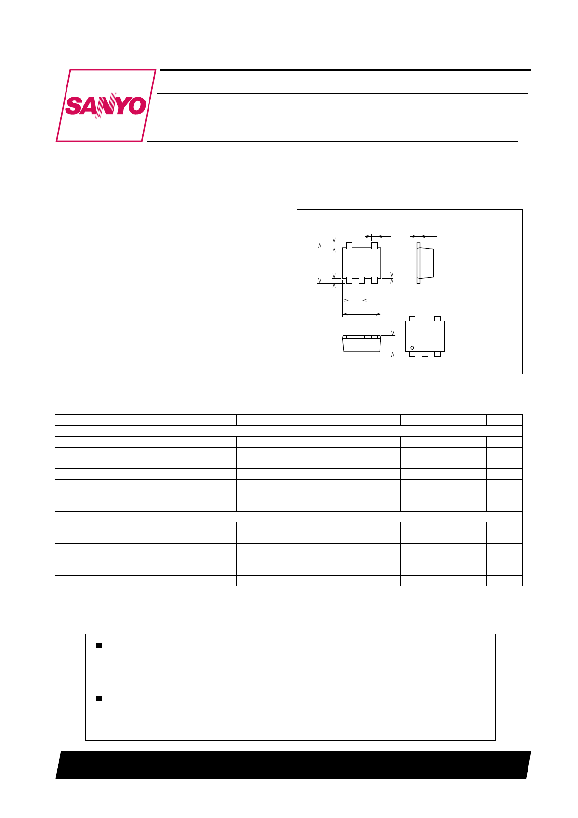
Package Dimensions
unit : mm
2195
[MCH5805]
0.250.25
4
2.1
1.6
0.65
0.3
5
132
0.07
2.0
0.85
0.15
54
123
1 : Gate
2 : Source
3 : Anode
4 : Cathode
5 : Drain
SANYO : MCPH5
Specifications
Absolute Maximum Ratings at Ta=25°C
Parameter Symbol Conditions Ratings Unit
[MOSFET]
Drain-to-Source Voltage V
Gate-to-Source Voltage V
Drain Current (DC) I
Drain Current (Pulse) I
Allowable Power Dissipation P
Channel T emperature T ch 150 °C
Storage T emperature Tstg --55 to +125 °C
[SBD]
Repetitive Peak Reverse Voltage V
Nonrepetitive Peak Reverse Surge Voltage V
Average Output Current I
Surge Forward Current I
Junction T emperature Tj --55 to +125 °C
Storage T emperature Tstg --55 to +125 °C
Marking : QE
DSS
GSS
D
DP
D
RRM
RSM
O
FSM
PW≤10µs, duty cycle≤1% --2.4 A
Mounted on a ceramic board (900mm2✕0.8mm) 1unit
50Hz sine wave, 1 cycle 2 A
--60 V
±20 V
--0.6 A
0.8 W
50 V
50 V
0.1 A
Any and all SANYO products described or contained herein do not have specifications that can handle
applications that require extremely high levels of reliability, such as life-support systems, aircraft's
control systems, or other applications whose failure can be reasonably expected to result in serious
physical and/or material damage. Consult with your SANYO representative nearest you before using
any SANYO products described or contained herein in such applications.
SANYO assumes no responsibility for equipment failures that result from using products at values that
exceed, even momentarily, rated values (such as maximum ratings, operating condition ranges, or other
parameters) listed in products specifications of any and all SANYO products described or contained
herein.
SANYO Electric Co.,Ltd. Semiconductor Company
TOKYO OFFICE Tokyo Bldg., 1-10, 1 Chome, Ueno, Taito-ku, TOKYO, 110-8534 JAPAN
N1501 TS IM TA-3399
No.7125-1/5
MCH5805
Electrical Characteristics at Ta=25°C
Parameter Symbol Conditions
[MOSFET]
Drain-to-Source Breakdown Voltage V
Zero-Gate Voltage Drain Current I
Gate-to-Source Leakage Current I
Cutoff Voltage VGS(off) VDS=--10V, ID=--1mA --1.2 --2.6 V
Forward Transfer Admittance
Static Drain-to-Source On-State Resistance
Input Capacitance Ciss VDS=--20V, f=1MHz 73 pF
Output Capacitance Coss VDS=--20V, f=1MHz 7 pF
Reverse Transfer Capacitance Crss VDS=--20V, f=1MHz 4 pF
Turn-ON Delay Time td(on) See specified Test Circuit. 6 ns
Rise Time t
Turn-OFF Delay Time td(off) See specified Test Circuit. 12.5 ns
Fall Time t
Total Gate Charge Qg VDS=--10V, VGS=--10V, ID=--0.6A 2.4 nC
Gate-to-Source Charge Qgs VDS=--10V, VGS=--10V, ID=--0.6A 0.6 nC
Gate-to-Drain “Miller” Charge Qgd VDS=--10V, VGS=--10V, ID=--0.6A 0.2 nC
Diode Forward Voltage V
[SBD]
Reverse Voltage V
Forward Voltage VF1I
Reverse Current I
Interterminal Capacitance C VR=10V, f=1MHz 4.4 pF
Reverse Recovery Time t
(BR)DSSID
DSS
GSS
yfs
RDS(on)1 ID=--0.3A, VGS=--10V 1.3 1.7 Ω
RDS(on)2 ID=--0.2A, VGS=--4V 1.6 2.3 Ω
r
f
SD
R
R
rr
=--1mA, VGS=0 --60 V
VDS=--60V, VGS=0 --1 µA
VGS=±16V, VDS=0 ±10 µA
VDS=--10V, ID=--0.3A 460 670 mS
See specified Test Circuit. 3.5 ns
See specified Test Circuit. 3 ns
IS=--0.6A, VGS=0 --0.88 --1.2 V
IR=50µA50V
=100mA 0.55 V
F
VR=25V 15 µA
IF=IR=100mA, See specified Test Circuit. 10 ns
Ratings
min typ max
Unit
Electrical Connection (Top view)
54
1 : Gate
2 : Source
3 : Anode
4 : Cathode
12 3
5 : Drain
Switching Time Test Circuit trr Test Circuit
[MOSFET] [SBD]
0V
--10V
PW=10µs
D.C.≤1%
G
VDD= --30V
ID= --0.3A
RL=100Ω
D
V
OUT
V
IN
V
IN
Duty≤10%
50Ω 100Ω 10Ω
10µs
--5V
100mA100mA
10mA
t
rr
P.G
50Ω
MCH5805
S
No.7125-2/5
 Loading...