

Page 1
FILE NO.
Service Manual
CONTENTS
–VOLUME +
CD Portable Radio
Cassette Recorder
MCD-ZX600F (XE)
(UK)
(PA)
321
654
987
BASS+100
PRODUCT CODE No.
164 129 00 XE
164 129 02 UK
164 129 03 PA
Laser beam safety precaution .......................................... 1
IC Block Diagram & Description ....................................... 1,9
Tuner Adjustments ........................................................... 2
Wiring Connection ........................................................... 3
Exploded View (Cabinet & Chassis) ................................ 4
Parts List .......................................................................... 6
Schematic Diagram .......................................................... 11
Wiring Diagram ............................................................... 18
Block Diagram .................................................................. 24
REFERENCE No. SM5810637
Page 2
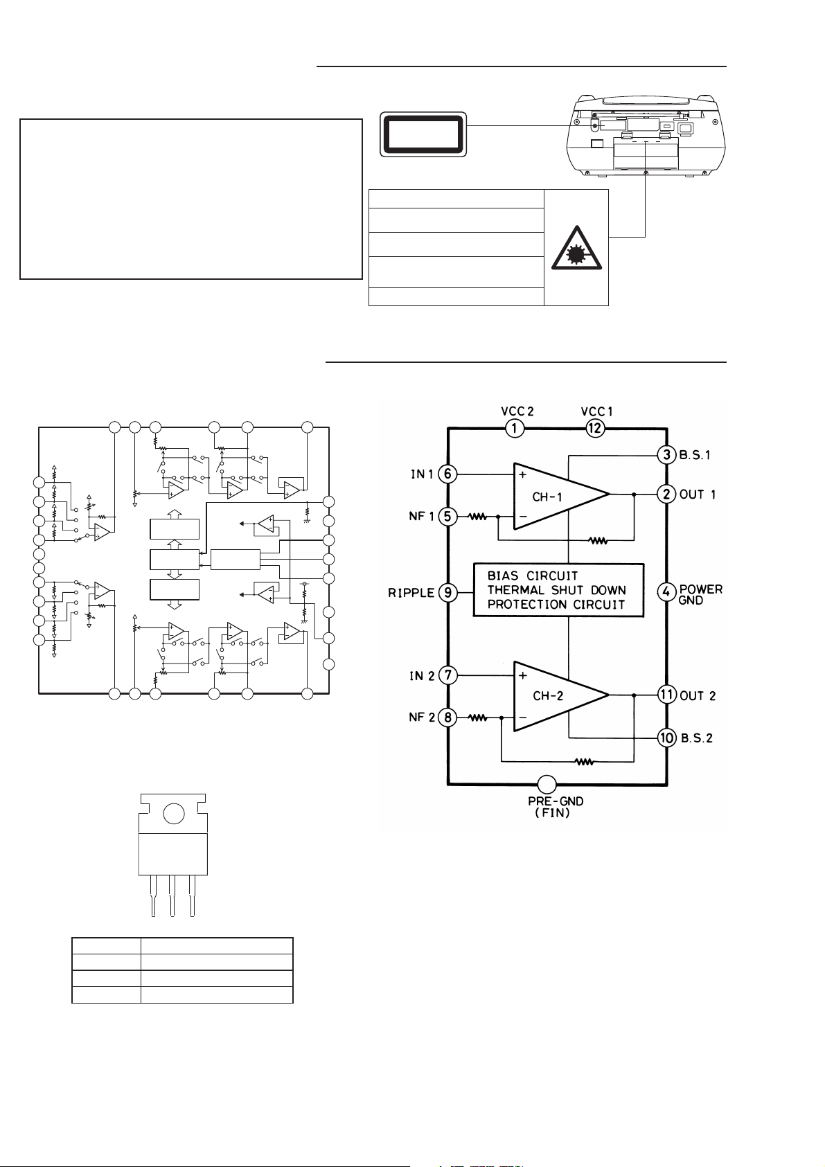
LASER BEAM SAFETY PRECAUTION
• Pickup that emits a laser beam is used on this CD section.
CAUTION :
USE OF CONTROLS OR ADJUSTMENTS OR
PERFORMANCE OF PROCEDURES OTHER
THAN THOSE SPECIFIED HEREIN MAY RESULT
IN HAZARDOUS RADIATION EXPOSURE.
LASER OUTPUT................ 0.6 mW Max. (CW)
WAVE LENGTH ................. 790 nm
IC BLOCK DIAGRAM & DESCRIPTION
LSELO LIN LTRE LBASS1 LBASS2 LOUT
10 9 7 6 58
CLASS 1 LASER PRODUCT
LUOKAN 1 LASERLAITE
KLASS 1 LASERAPPARAT
CAUTION-INVISIBLE LASER RADIATION WHEN OPEN AND
INTERLOCKS DEFEATED. AVOID EXPOSURE TO BEAM.
ADVARSEL-USYNLIG LASER STRÅLING VED ÅBNING, NÅR
SIKKERHEDSAFBRYDERE ER UDE AF FUNKTION, UNDGÅ
UDS ÆTTELSE FOR STRÅLING.
VARNING-OSYNLIG LASER STRÅLNING NÄR DENNA DEL
ÄR ÖPPNAD OCH SPÄRR ÄR URKOPPLAD. STRÅLEN ÄR
FARLIG.
VORSICHT! -UNSICHTBARE LASERSTRAHLUNG TRITT
AUS, WENN DECKEL GEÖ FFNET UND ENN
SICHERHEITSVERRIEGELUNG ÜBERBRÜCKT IST. NICHT,
DEM STRAHL AUSSETZEN.
VARO !-Avattaessa ja suojalukitus ohitettaessa olet alttiina
näkymättömälle lasersäteilylle. Älä katso säteeseen.
IC301 TA8227 (Power Amp.)IC501 LC75342(Function SW)
L4
11
L3
12
L2
13
L1
14
NC
15
NC
16
R1
17
R2
18
R3
19
R4
20
21 22 24 25 2623
RSELO RIN RTRE RBASS1 RBASS2 ROUT
CONTROL
CIRCUIT
LOGIC
CIRCUIT
CONTROL
CIRCUIT
LVref
CCB
INTERFACE
RVref
IC401 KIA7808(Voltage Regulator)
4
TEST
3
SS
V
2
CE
1
DI
30
CL
29
DD
V
28
Vref
27
NC
1 2 3
Pin No. Function
1 INPUT
2COMMON
3
OUTPUT
- 1 -
Page 3
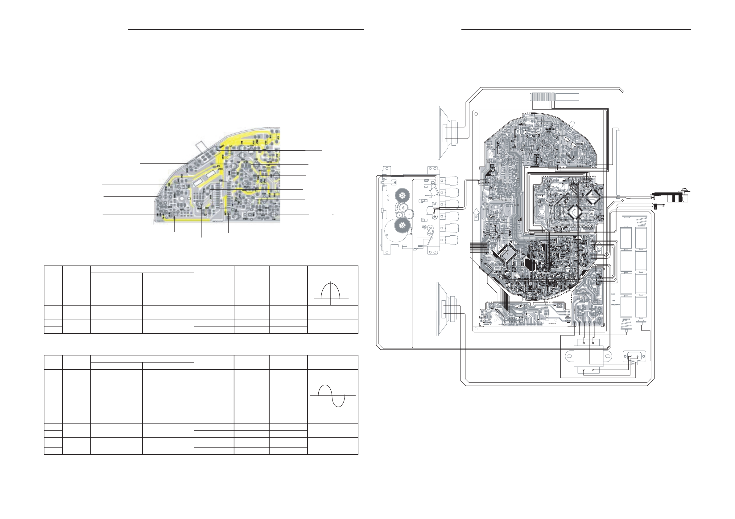
TUNER ADJUSTMENTS WIRING CONNECTION
Use a plastic screw driver for adjustments.
Adjust the intermediate frequency of AM and FM to the frequency of ceramic filter.
Set of unit
Supply voltage : DC 12.0V
Speaker impedance : 8 ohms
Standard output : 50 mW
Function switch : RADIO
a. Parts Location
BIAS O/N
RESET O/N
L102
CT101
FM/ANT
AM/ANT
L101
OUT
a. AM Adjustment Band switch : MW
Adjusting Connections
Step Adjustment
Circuit lnput Output
Closed the output
terminal by sweep
1
2
3
4
5
IF generator to(19)IC101 450KHz Low T103
generator,it place
to AM ANT
Tuning Connect AM SG to Connect VTVM to 522 KHz Low end T101 VT Low: 1.5V±0.1
coverage test loop speaker terminals. 1611 KHz High end VT Hi: 7.5V±0.2
Tracking
Connect AM SG to Connect VTVM to 603 KHz 603 KHz MW ANT
test loop speaker terminals 1404 KHz 1404 KHz CT102
Connect sweep
(H) 0and C130(E)
SG
Frequency
Position of VTVM
Tuning dial Oscilloscope
450KHZ
T103/2070
10.7MHZ
T101/612R
CT102
Max.
b. FM Adjustment Band switch : FM FM Dummy antenna : 75 ohms unbalance
Adjusting Connection position of VTVM
Step SG Frequency
Circuit Input Output tuning dial Oscilloscope
Connect sweep Connect VTVM to
1
2
3
4
5
IF generator to IC101 generator to (19) 10.7MHz Low
(22)pin (H) & IC101(H) and C130(E)
IC101(23)pin (E)
Tuning Connect FM SG to Connect VTVM to 87.5 MHz Low end L102 VT Low : 2.1V±0.1
coverage FM ANT(H) D101 speaker terminals. 108 MHz High end VT Hi : 7.2V±0.1
Tracking
Connect FM SG to Connect VTVM to 90.0 MHz 90.0 MHz L101
FM ANT(H) D101 speaker terminals. 106.0 MHz 106.0 MHz CT101
Adjustment
This is a basic tuner adjustments.
Max.
This is a basic wiring connection.
- 3 -- 2 -
Page 4
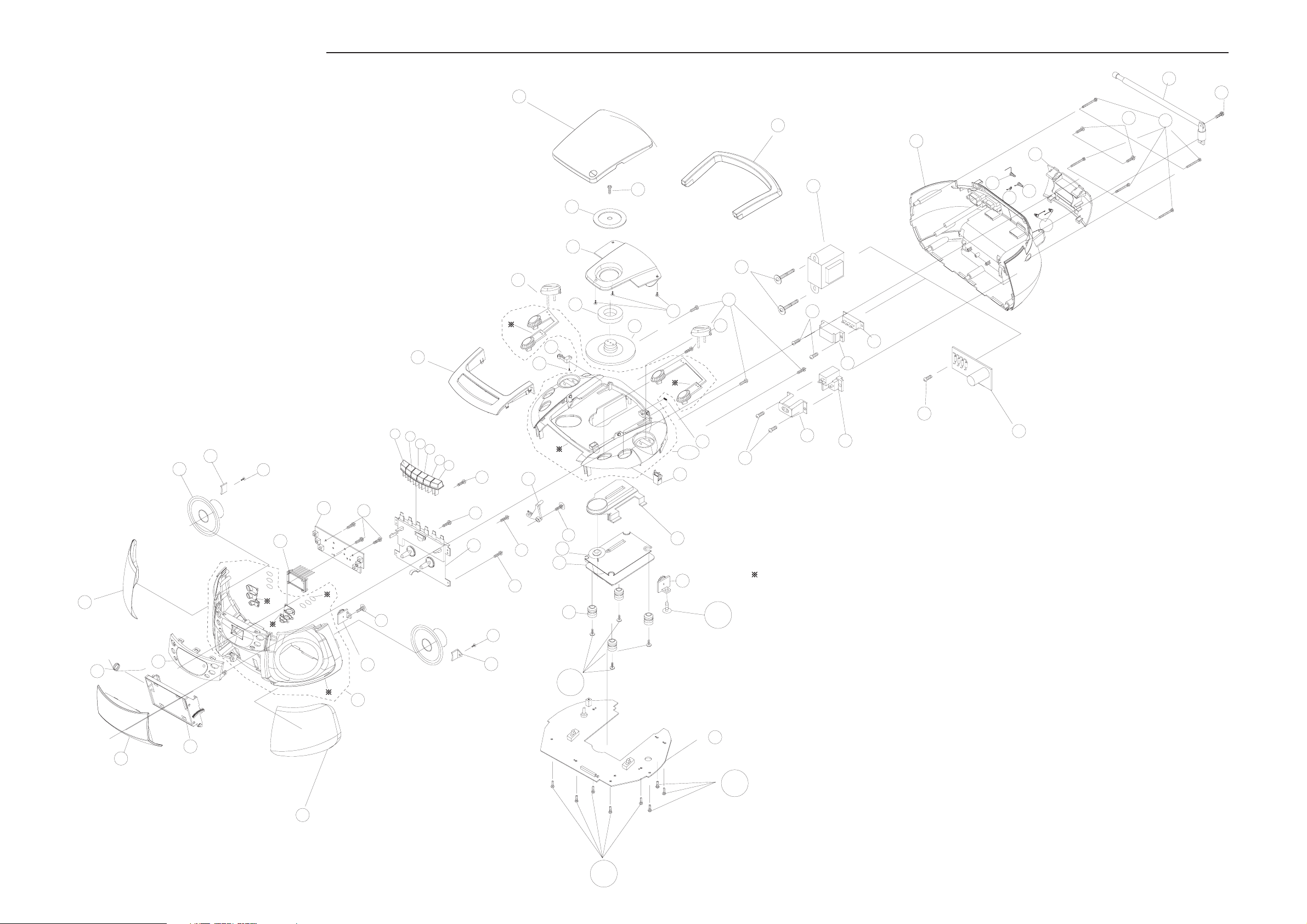
EXPLODED VIEW(CABINET & CHASSIS)
24
42
Y18
65
12
38
Y16
Y17
41
43
44
45
46
25
Y6
62
47
26
Y14
29
48
30
Y8
Y13
64
39
Y15
73
Y12
40
63
27
Y7
28
22
61
Y9
31A
37
23
16
17
18
19
20
Y1
21
Y4
71
11
Y3
Y4
15
Y5
Y4
34
33
74
Y4
36
: Not available as service parts.
5
Y2
Y1
3
4
14
13
35
Y10
Y19
7A
72
2
1
Y11
6
Y11
- 5 -- 4 -
Page 5

PARTS LIST
PARTS LIST
PRODUCT SAFETY NOTICE
EACH PRECAUTION IN THIS MANUAL SHOULD BE FOLLOWED DURING SERVICING. COMPONENTS IDENTIFIED WITH
!!
!
THE IEC SYMBOL
CAN OF SPECIAL SIGNIFICANCE. WHEN REPLACING A COMPONENT IDENTIFIED , USE ONLY THE REPLACEMENT
PARTS DESIGNATED, OR PARTS WITH THE SAME RATINGS OF RESISTANCE, WATTAGE OR VOLTAGE THAT ARE
DESIGNATED IN THE PARTS LIST IN THIS MANUAL. LEAKAGE-CURRENT OR RESISTANCE MEASUREMENTS MUST
BE MADE TO DETERMINE THAT EXPOSED PARTS ARE ACCEPTABLY INSULATED FROM THE SUPPLY CIRCUIT BEFORE
RETURNING THE PRODUCT TO THE CUSTOMER.
CAUTION : Regular type resistors and capacitors are not listed. To know those values, refer to the schematic diagram.
PACKING & ACCESSORIES
REF.NO. PART NO. DESCRIPTION
!!
!
!!
!
!!
!
CABINET & CHASSIS
REF.NO. PART NO. DESCRIPTION
1 645 072 3254 CASS DOOR
2 645 072 3322 CASS DOOR BRACKET
3 645 062 0478 CASS DOOR SPRING
4 645 070 9272 DISPLAY LENS
5 645 069 7364 SPEAKER GRILL LEFT
6 645 069 7371 SPEAKER GRILL RIGHT
7A 645 072 1984 ASSY FRONT CABINET
11 645 072 3421 LCD BRACKET
12 645 072 3339 SPEAKER CLIP L
13 645 072 3346 SPEAKER CLIP R
14 645 072 3360 CASS DOOR GEAR
16 645 072 3261 KNOB CASS PAUSE
17 645 072 3278 KNOB CASS STOP/EJECT
18 645 072 3285 KNOB CASS FFWD
19 645 072 3292 KNOB CASS REWIND
20 645 072 3308 KNOB CASS PLAY
21 645 072 3315 KNOB CASS RECORD
22 645 069 7166 RECORDING BRACKET
23 645 070 9258 DISPLAY PANEL
24 645 072 3353 CD DOOR LENS
25 645 033 3996 CD CHUCK M
26 645 069 7210 CD DOOR
27 645 033 3972 CD MAGNET RING
28 645 033 3989 CD CHUCK A
29 645 072 3391 KNOB VOLUME,ROTARY
30 645 072 3384 KNOB TUNING,ROTARY
31A 645 072 1991 ASSY TOP CABINET
33 645 042 0375 CD MECHA COVER
34 645 069 6893 CD DECK MECHANISM
35 645 033 3446 RUBBER SILICON,FOR CD DECK
36 645 069 7289 GEAR HOLDER,
37 645 043 0145 CD DOOR LOCK
38 645 070 9111 HANDLE
39 645 042 0368 BAND SW COVER(PA)
40 645 033 0391 AC SKT COVER
41 645 070 9081 CABINET BACK
IN THE PARTS LIST AND THE SCHEMATIC DIAGRAM DESIGNATE COMPONENTS IN WHICH SAFETY
Regular type resistors are less than 1/4W carbon type and 0 ohm chip resistors.
Regular type capacitors are less than 50V and less than 1000µF of Ceramic type and Electrolytic type.
REF.NO. PART NO. DESCRIPTION
43 645 070 9104 BATTERY DOOR
44 645 070 9319 BATTERY SPRING+
645 072 3537 GIFT BOX(PA)
645 072 3520 GIFT BOX(UK)
645 072 3513 GIFT BOX(XE)
645 072 3452 INSTRUCTION MANUAL(PA)
645 072 3445 INSTRUCTION MANUAL(UK)
645 072 3438 INSTRUCTION MANUAL(XE)
645 066 6063 POLY BAG,I/B
645 070 9296 POLY BAG,PWR CORD
645 069 7357 POLY BAG,UNIT
645 072 3476 POLY FOAM,
1KIT 2 PCS LEFT&RIGHT
645 071 9813 POWER CORD(PA)
645 069 6534 POWER CORD,VDE(XE)
645 062 5862 PWR CORD,BSI(UK)
645 072 2004 REMOTR CONTROL,
RC25-102035-010
45 645 033 0926 BATT SPRING(+)
46 645 071 9981 BATTERY SPRING47 645 070 9302 BATTERY SPRING48 645 042 0351 CD DOOR SPRING
FIXING PARTS
REF.NO. PART NO. DESCRIPTION
Y1 645 027 1168 SCR 3X8,SPEAKER CLIP L
Y2 645 069 6794 SCREW 3X10,CASS DOOR GEAR
Y3 645 023 6594 SCREW ST 3X8,CONTROL PCB
Y4 645 069 6787 SCREW 3X10,CASS DECK
Y5 645 069 6794 SCREW 3X10,
RECORDING BRACKET
Y6 645 051 6641 SCR 2 X 6,
CD CHUCK M TO CD CHUCK A
Y7 645 062 1086 SCR 2X5,CD DOOR
Y8 645 069 6787 SCREW 3X10,
TOP CAB TO FRONT CAB
Y9 645 072 2394 SCREW 2X6,LEAF SWITCH
Y10 645 027 1168 SCR 3X8,CD DOOR GEAR
Y11 645 023 6594 SCREW ST 3X8,MAIN PCB
Y12 645 027 1144 SCR 2.8X12,
AC SKT COVER TO AC SKT
Y13 645 023 6594 SCREW ST 3X8,
VOL. SELE.COVER TO VOL.S(PA)
Y14 645 027 1182 SCR 3X20,POWER TRANSFORMER
Y15 645 023 6594 SCREW ST 3X8,RECTIFER BOARD
Y16 645 023 6617 SCREW ST 3X10,
TOP CAB TO BACK CAB
Y17 645 027 3841 SCR 3X2.5,
BACK CAB TO FRONT CAB
Y18 645 027 1236 SCR 3X8,ROD ANTENNA
Y19 645 069 6770 SCREW 2.6X8,CD DECK
ELECTRICAL-PARTS
REF.NO. PART NO. DESCRIPTION
42 645 070 9043 ROD ANTENNA
61 645 069 6657 LEAF SWITCH,CD LID SW
62
62
63 645 032 9760 AC SOCKET S-1-1225,VDE
64 645 069 6534 POWER CORD(PA)
64 645 023 6358 SW SLIDE SS12J01M65,
65 645 069 6558 SPEAKER
FOR CASS DOOR GEAR
!!
!
645 069 6541 POWER TRANSFORMER(UK)(XE)
!!
!
645 071 9837 POWER TRANSFORMER,
110/220V(PA)
100/220V(PA)
645 072 2325 5P HSG,
645 072 2400 5P HSG,
645 072 2417 6P HSG,
645 072 2332 FFC CABLE 11P,
MAIN CN201 TO CASS DECK
MAIN CN906 TO CD BD CN90
MAIN CN401 TO REFCT.CN40
MAIN CN701 TO CD BD CN9
PARTS LIST
REF.NO. PART NO. DESCRIPTION
645 072 2349 FFC CABLE 15P,
MAIN CN702 TO CTL CN704
645 072 2356 FFC CABLE 18P,
MAIN CN703 TO CTL CN705
645 072 3223 SHIELD PLATE,
FOR SPEAKER GRILLE
645 027 1342 SOLDERING BAR 60/40
645 027 1328 SOLDERING SLUG
645 027 1359 SOLDERING WIRE
645 033 3606 FERRITE BEAD,CN403
645 033 3606 FERRITE BEAD,CN902
645 033 3606 FERRITE BEAD,
POWER OUT PUT WIRE
645 072 2318 3P HSG,
RECTI. CN403TO CASS DECK
645 069 6732 4P HSG,MAIN CN301 TO SPEAKER
CONTROL P,W,BOARD ASSY
REF.NO. PART NO. DESCRIPTION
71 614 332 1330 ASSY,PWB CONTROL(Only initial)
CN704 645 033 3675 FFC HEADER 15PINS
CN705 645 069 6695 HEADER FFC 18P
IR701 645 033 3477 DIODE RPM-6938-V4
SW704 645 042 0023 SW TACT,TU PRESRT,REPEAT
SW705 645 042 0023 SW TACT,MEMORY
SW707 645 042 0023 SW TACT,STOP
SW708 645 042 0023 SW TACT,TUNING+
SW709 645 042 0023 SW TACT,PLAY,PAUSE
SW710 645 042 0023 SW TACT,TUNING-
645 072 3421 LCD BRACKET
645 072 2264 LCD DISPLAY
645 072 3230 SHIELD PLATE,FOR CONTROL PCB
645 062 0010 BUFFER FOR FFC CABLE,
FOR FFC CABLE
MAIN P.W.BOARD ASSY
REF.NO. PART NO. DESCRIPTION
72 614 332 1323 ASSY,PWB MAIN(Only initial)
C0003 645 072 2233 POLYESTER 0.0082U 100V,C501(-)
C0004 645 072 2233 POLYESTER 0.0082U 100V,C502(-)
C0206 645 034 9805 MYLAR CAP 0.001 UF/1
C0207 645 034 9805 MYLAR CAP 0.001 UF/1
C0212 645 072 2240 POLYESTER 0.033U 50V
C0213 645 072 2240 POLYESTER 0.033U 50V
C0218 645 072 2219 POLYESTER 0.0018U 100V
C0219 645 072 2219 POLYESTER 0.0018U 100V
C0311 645 034 9898 MYLAR CAP 0.1 UF/10
C0312 645 034 9898 MYLAR CAP 0.1 UF/10
C0313 645 034 9751 ELECT CAP 1000 UF/16
C0314 645 034 9751 ELECT CAP 1000 UF/16
C0513 645 072 2226 POLYESTER 0.0027U 100V
C0514 645 072 2226 POLYESTER 0.0027U 100V
C0709 645 055 6784 GOLD CAP DX-5R5H104
C0965 645 034 9829 MYLAR CAP 0.0022 UF/
C0966 645 034 9829 MYLAR CAP 0.0022 UF/
CF101 645 051 6467 BAND PASS FILTER
CF102 645 055 6913 CERAMIC FILTER
CF103 645 055 6913 CERAMIC FILTER
CF104 645 055 6906 CERAMIC FILTER
CF105 645 055 6920 CERAMIC FILTER
CN201 645 054 0660 5P HEADER
CN301 645 054 0653 4P HEADER
CN701 645 072 2295 FFC HEADER 11P
CN702 645 033 3675 FFC HEADER 15PINS
CN703 645 072 2301 FFC HEADER 18P
CT101 645 072 2257 TRIMMER 20PF
CT102 645 072 2257 TRIMMER 20PF
D0101 645 023 6099 DIODE 1N-4148
D0102 645 023 6099 DIODE 1N-4148
D0105 645 023 6099 DIODE 1N-4148
D0106 645 023 6099 DIODE 1N-4148
D0301 645 023 6099 DIODE 1N-4148
D0302 645 023 6099 DIODE 1N-4148
REF.NO. PART NO. DESCRIPTION
D0303 645 023 6112 RECTIFIER 1N-4001
D0304 645 023 6099 DIODE 1N-4148
D0305 645 023 6099 DIODE 1N-4148
D0306 645 023 6099 DIODE 1N-4148
D0307 645 023 6099 DIODE 1N-4148
D0308 645 023 6099 DIODE 1N-4148
D0309 645 023 6099 DIODE 1N-4148
D0310 645 023 6099 DIODE 1N-4148
D0311 645 023 6099 DIODE 1N-4148
D0312 645 023 6099 DIODE 1N-4148
D0313 645 023 6112 RECTIFIER 1N-4001
D0314 645 023 6112 RECTIFIER 1N-4001
D0402 645 023 6099 DIODE 1N-4148
D0701 645 023 6099 DIODE 1N-4148
D0703 645 023 6099 DIODE 1N-4148
D0706 645 023 6099 DIODE 1N-4148
D0709 645 023 6099 DIODE 1N-4148
D0711 645 023 6099 DIODE 1N-4148
D0713 645 023 6099 DIODE 1N-4148
D0715 645 023 6099 DIODE 1N-4148
D0716 645 023 6099 DIODE 1N-4148
D0717 645 023 6099 DIODE 1N-4148
D0718 645 023 6099 DIODE 1N-4148
D0722 645 023 6099 DIODE 1N-4148
IC101 645 055 6975 IC LA1823ESIA
IC102 645 055 7019 IC LC72131
IC201 645 055 6999 IC TA8142AP
IC301 645 034 9980 IC TA-8227P TOSHIB
IC402 645 055 7033 IC S-81256SGYX
IC501 645 055 7026 IC LC75342
IC701 645 066 5806 IC LC587008 1P55
IC702 645 055 6951 IC PST600C
IC703 645 055 6968 IC PST600L
JK301 645 035 0429 STEREO TYPE EARPHONE
L0101 645 023 6297 VHF COIL
L0102 645 027 0345 VHF COIL
L0105 645 027 0352 CHOKE COIL 100UH
L0301 645 062 0850 FERRITE BEAD
L0302 645 062 0850 FERRITE BEAD
L0303 645 062 0850 FERRITE BEAD
L0501 645 027 0352 CHOKE COIL 100UH
L0701 645 027 0352 CHOKE COIL 100UH
L0702 645 027 0352 CHOKE COIL 100UH
Q0107 645 034 6866 TR 2SC2839E
Q0108 645 034 7078 TR 2SC3330U
Q0109 645 027 0420 TR 8050C
Q0110 645 055 6876 TR 9018F
Q0301 645 072 3162 TRANSISTOR 9014C
Q0302 645 072 3162 TRANSISTOR 9014C
Q0303 645 072 3162 TRANSISTOR 9014C
Q0304 645 023 6129 TR 9014C
Q0305 645 023 6129 TR 9014C
Q0403 645 055 6883 TR KSA928A
Q0404 645 072 3162 TRANSISTOR 9014C
Q0405 645 027 0420 TR 8050C
Q0407 645 055 6869 TR 8550B C
Q0408 645 072 3162 TRANSISTOR 9014C
Q0409 645 027 0420 TR 8050C
Q0701 645 072 3155 TRANSISTOR DTA114TS
Q0704 645 072 3155 TRANSISTOR DTA114TS
Q0705 645 072 3179 TRANSISTOR 2SC3400AC
Q0706 645 072 3179 TRANSISTOR 2SC3400AC
Q0707 645 072 3155 TRANSISTOR DTA114TS
Q0708 645 072 3179 TRANSISTOR 2SC3400AC
Q0709 645 072 3155 TRANSISTOR DTA114TS
Q0710 645 072 3155 TRANSISTOR DTA114TS
Q0711 645 072 3155 TRANSISTOR DTA114TS
Q0712 645 072 3155 TRANSISTOR DTA114TS
Q0801 645 027 0420 TR 8050C
Q0803 645 023 6129 TR 9014C
R0326 645 072 2172 RESISTOR 10 OHM 1/2W
S0001 645 042 0023 SW TACT,POWER
SW010 645 042 0023 SW TACT,BASS
- 7 -- 6 -
Page 6

PARTS LIST
IC BLOCK DIAGRAM & DESCRIPTION
REF.NO. PART NO. DESCRIPTION
SW100 645 055 7064 SW TACT,RESET
SW201 645 023 6327 SW RECORDING PS62D01-S(SH
SW701 645 042 0023 SW TACT,TAPE
SW702 645 042 0023 SW TACT,TUNER/BAND
SW703 645 042 0023 SW TACT,FM MODE
SW712 645 042 0023 SW TACT,VOL-DOWM
SW713 645 042 0023 SW TACT,VOL-UP
SW714 645 042 0023 SW TACT,RANDOM
SW801 645 024 1048 SW SLIDE SK22F03G6,
BEAT CANCEL
T0101 645 055 6944 IFT,OSC 1A612R
T0103 645 033 3866 AM COIL,IF 2070
T0801 645 027 0307 BIAS COIL,AC BIAS 3630
VD101 645 055 6807 DIODE SVC201
VD102 645 055 6807 DIODE SVC201
VD103 645 055 6814 DIODE SVC348
X0101 645 055 7118 CRYSTAL
X0701 645 072 2288 CRYSTAL 4MHZ
X0702 645 062 0911 CRYSTAL 32.768KHZ
ZD101 645 055 6838 ZENER 5.6V
ZD401 645 055 6845 ZENER 13V
645 070 9050 HEAT SINK,FOR IC 301
645 072 3216 CONTACT PIN
645 072 3247 SHIELD PLATE,IC102
645 061 9946 1P HSG,FM ANT
645 072 1977 ASSY BAR ANT
RECTIFIER P.W.BOARD ASSY
REF.NO. PART NO. DESCRIPTION
73 614 332 1347 ASSY,PWB RECTIFIER(Only initial)
CN402 645 061 9922 6P HEADER
CN403 645 033 3682 HEADER 3PINS
D1101 645 023 6112 RECTIFIER 1N-4001
D1102 645 023 6112 RECTIFIER 1N-4001
D1103 645 023 6112 RECTIFIER 1N-4001
D1104 645 023 6112 RECTIFIER 1N-4001
F1101 645 054 0639 FUSE GLASS TUBE,FS1101
IC401 645 055 6982 IC KIA7808P
JP413 645 023 6112 RECTIFIER 1N-4001
Q0401 645 055 6883 TR KSA928A
Q0402 645 023 6129 TR 9014C
645 035 0511 FUSE HOLDER MW1010K,
FOR FS1101
645 027 1298 EYELET
645 042 0320 HEAT SINK,FOR IC401
CD P.W.BOARD ASSY
REF.NO. PART NO. DESCRIPTION
74 614 332 1354 ASSY,PWB CD(Only initial)
CN901 645 055 7163 16P FFC HEADER
CN902 645 054 0660 5P HEADER
CN903 645 072 2295 FFC HEADER 11P
CN904 645 051 6511 2P HEADER
IC901 645 072 3186 IC LA9242M
IC902 645 072 3193 IC LC78629E
IC903 645 069 6879 IC LA6541D
J0907 645 069 6886 INDUCTOR 2.7UH
L0901 645 042 0108 CHOKE COIL 26UH
Q0901 645 033 3491 TR 2SC945P
Q0905 645 061 8246 TR 2SA608NFNPAAT
Q0907 645 033 3514 TR 2SB764D
W106 645 072 2387 J WIRE AWG28,
IC902 PIN59 TO GND
X0901 645 072 2271 CRYSTAL 16.9344MHZ
ZD901 645 044 6924 ZENER DIODE 3.9V
645 042 0337 HEAT SINK,FOR IC903
DECK MECHANISM ASSY
REF.NO. PART NO. DESCRIPTION
15 645 072 1762 CASS DECK MECHANISM
645 069 6442 MOTOR ASSY
645 069 6473 PINCH ROLLER ASSY
645 058 9553 RF BELT
645 069 6626 MAIN BELT
645 030 6839 E HEAD
645 018 0637 R/P HEAD
IC903 LA6541 (CD Driver) IC101 LA1823 (Tuner)
Vcc Vref VIN4 VG4 Vo8 Vo7 GND Vo6 Vo5 VG3 VIN3 CD RES
11k Ω 11k Ω
Level
Sift
Level
Sift
123 456 789
Vcc Mute VIN1 VG1 Vo1 Vo2 GND Vo3 Vo4 VG2 VIN2 Reg OUT Reg IN
BTL
Driver
BTL
Driver
Vcc
BTL
Driver
BTL
Driver
Level
Sift
Level
Sift
11k Ω11k Ω
10 11 12
131415161718192021222324
RESET
Regulator
IC901 LA9242M (Servo)
-
+
20
FE
FA-
31 SL+
32 JP-
33 JP+
34 TGL
35 TOFF
36 TES
37 HFL
38 SLOF
39 CV-
40 CV+
LF2
59
2221
FE-
VR
REF1
56
57
58
REF
U-COM
INTER FACE
SPINDLE SERVO
25
23
24
SP
NC
AGND
41 RFSM
42 RFS-
43 SLC
44 SLI
45 DGND
46 FSC
47 TBC
48 NC
49 DEF
50 CLK
VCC2
SPG
CL
FSS
CE
CLK
DRF
DAT
DEF
49
525150
55
54
53
48
NC
47
46
SLC
45
44
-
+
43
SLC
42
RFS-
-
+
41
RF Amp
SLED SERVO
-
+
26
SP-
27
SPD
28
SLEQ
51 CL
52 DAT
53 CE
54 DRF
55 FSS
56 Vcc2
57 REF1
58 VR
59 Lf2
60 Ph1
+
29
SLD
RFSM
40
CV+
39
38
SLOF
37
36
TES
35
TOFF
34
TGL
33
-
32
3130
SL-
JP-
SL+
61 BH1
62 LDD
63 LDS
64
Vcc1
IC102 LC72131 (PLL)
TBC
FSC
DGND
SLI
CV-
HFL
JP+
IC702,703 PST600 (Voltge Regulator)
VCC1
64
FIN2
1
FIN1
2
I/V
E
3
F
4
5
TB
TE-
6
TE
7
TESI
8
9
SCI
10
TH
11
TA
12
TD-
-
13
TD
14
JP
15
TO
16
FD
PIN FUNCTION
1 FIN2
2 FIN1
3 E
4 F
5 TB
6 TE-
7 TE
8 TESI
9 SCI
10
11 TA
12 TD-
13 TD
14 JP
15 TO
16 FD
17 FD-
18 FA
19 FA-
20
TH
LDS
63
APC
+
-
T.SERVO & T.LOGIC
+
FE
LDD
62
TE
21 FE-
22 AGND
23 NC
24 SP
25 SPG
26 SP-
27 SPD
28 SLEQ
29 SLD
30 SL-
PH1
BH1
60
61
VCA
VCABAL
F.SERVO & F.LOGIC
+
-
17
18
FA
FD-
RF DET
+
-
19
IC402 S-81256SGYX (Voltge Regulator)
Top view
1. GND
IN
2
V
IN
2
2. V
31
3. V
OUT
3
OUT
V
1
2
3
1
Vcc
Vout
3
2
GND
1
2
3
VCC
GND
Vout
GND
REFERENCE
VOLTAGE
1
- 9 -- 8 -
Page 7

IC BLOCK DIAGRAM & DESCRIPTION
IC701 LC587008(4 bit Micro processor)
Address
SCHEMATIC DIAGRAM (RADIO)
V
DD
V
SS
V
1
DD
2
V
DD
CUP1
CUP2
Input
CFIN
Output
CFOUT
XTIN Input 20
Output
XTOUT
S1
S2
Input
S3
S4
K1
K2
I/O
K3
K4
M1
M2
I/O
M3
M4
A1
A2
I/O
A3
A4
P1
P2
I/O
P3
P4
Pin No.
24
Power supply
23
LCD drive power supply
22
VDD
21
VDD1
VDD2
VSS
Switching pin used to supply theLCD drive voltage to the VDD1 and
V2PINS
DD
3
Connect a nonpolarized capacitor between CUP1 and CUP2 when
4
1/2 or 1/3 bias is used
Leave open when a bias other than 1/2 or1/3 is used.
System clock oscillator connections
25
Ceramic resonator connection (CF specifications)
RC component connection (RC specifications)
External signal input pin (CFOUT isleft open)
26
This oscillator isstopped by the execution of aSTOP or SLOW
instruction.
Referenc e calculation(cl ock specification s,LCD alternain g frequency),
system clock oscillator
32 kHz crystal resonator connection
65 kHz crystal resonator connection
19
This oscillator isstopped by the execution of aSTOP instruction.
Input-only ports
Input pins used to read data into RAM
27
Built-in 7.8 msand 1.95 ms chatter rejection circuits
28
Built-in pull-up/pull-down resistors
29
Note: The 7.8 ms and 1.95 ms times are the times when f 0is
30
32.768kHz.
I/O ports
Input pins used to output readdata into RAM
31
Output pins used to output data from RAM
32
Built-in 7.8 msand 1.95 ms input-mode chatter rejection circuits.
33
The selection of 7.8 or 1.95 ms is linked to that for the S ports.
34
Note: The 7.8 ms and 1.95 ms times are the times when f 0is
32.768 kHz.
I/O ports
35
Input pins used to read data into RAM
Output pins used to output data from RAM
36
M4 is used as the external clock input pinin Tm2 mode 3.
37
*The minimum period for the external clock is twice the cycle time.
38
Built-in pull-up/pull-down resistors
11
I/O ports
12
Input pins used to read data into RAM
Output pins used to output data from RAM
13
Built-in pull-up/pull-down resistors
14
15
I/O ports
16
Function: The same as pins A1 to A4
17
18
Function
NON 1/1 bias
1/2 bias
1/3 bias
CF specifications
RC specifications
External
Specifications
Not used
32k specifications
65k specifications
38k specifications
Not used
Transistor to hold
a low or high level
Selection of either
pull-up or pulldown resistor
Transistors to hold
a low or high level
Selection of either
pull-up or pulldown resistor
The same as K1 toK4The same as K1 to
The same as K1 to
K4
The same as K1 to
K4
Option
At reset
The pull-up orpulldown resistor are
on.
Note:
These pin sgo
to the floatin g
state when
reset is cle ared.
The pull-up orpulldown resistors are
on.
Note:
These pin s go
to the floatin g
state when
reset is cle ared.
Input mode
Output latch data is
set high.
K4
The same as K1 to
K4
The same as K1 to
K4
Continued from preceding
I/O
Pin
So1
So2
I/O
So3
So4
N1
N2
Output
N3
N4
INT
Input
RES
Input
TST
Input
Seg1,
Seg2 to
Output
Seg35
COM1
COM2
Output
COM3
COM4
page.
QIP-80
Pin No.
I/O ports
Function: The same as for pins A1 to A4
Pins So1 to So3 area alsoused for theserial interface.
7
Use of these pins inserial mode can be selected under program
8
cotrol.
9
Pin functions: SO1:Serial input pin
10
The serial clock pin can be switched between internal and external,
and between rising edge output andfalling edge output.
Output-only ports
Output pins used to output data from RAM
39
An alarm signal can be output from pin N4.(Note that this is only
40
when the N 4output latch islow.)
41
An alarm signal modulated at 1,2 or 4 kHz can be output.(These
42
frequencies are output when f 0 is 32.768 kHz.)
A carrier signal can be output from N3.(Note that this is only
when the N3 output latch islow.)
Input ports
External interrupt request inputs
Input pins used to read datainto RAM
6
Input detection can be performed oneither rising or falling edges.
Built-in pull-up/pull-down resistors
LSI internal reset input
The reset input level can be selected to be either high or low.
5
Built-in pull-up/pull-down resistors
Note: The reset pulse must beat least 500us.
Tes t i np u t
QIP80 products: Connect to Vss.
43
Chip products : Leave open or connect to Vss.
LCD panel drive/general-purpose
LCD panel drive
STATIC
1/2 bias-1/2 duty
1/2 bias-1/3 duty
1/2 bias-1/4 duty
1/3 bias-1/3 duty
1/3 bias-1/4 duty
Types I to V can be specified asmask
44,
General-purpose output mode
45 to
CMOS
78
P-channel open drain
N-channel open drain
Types I to III can be specified asmask options.
LCD/general -purpo se output contro l is handled by the segme nt PLA,
and thus program control is not required.
These pins support output latch control on reset and in standby
states when the oscillators are stopped.
Arbitrary com binations of LCD drive and gene ral-purpos e output s can
be used.
LCD panel drive common polarity outputs
The table below shows how these pins are used depen ding on the duty
used.( values for alterna ting freque ncy reflect a typical specif ication of
32.768 MHz for f 0.)
2
1
COM1
COM2
80
79
COM3
COM4
Alternation
frequency
Note: A cros s( X ) indicates that the pin is not used with that duty type.
SO2:Serial output pin
SO3:Serial clock pin
Static duty
32 Hz32 Hz
Function
1/2 duty
32 Hz
output
1/3 duty
42.7 Hz
options.
The same as for K1
to K4
type:
The output level s on
pins N1 to N4 can be
specified as an opti on
LCD drive
*:Determined by
mask options
General purpose
outputs
Note:
These pins go to
the static drive
mode during the
reset
The static drive
waveform is output
during the reset
period.
*There are cases
where the
alternati ng
frequenc y stops for
the CF,RC and
external clock
specifica tions.
(These cases differ
dependi ng on option
specifica t
At reset
All segment s on
All segm ents off
High level
Low level
Determined by
mask options
When a
combinatio n of
LCD drive and
general-
purpose
outputs,the
output state is
either:
All lit/hig h level
All off/low level.
period.
ions.)
Option
Tran sis tors to hol d
a low or high leve l
Selecti on of either
pull-up or pulldown resis tors
Interna l serial clock
divisor selecti on
I1/1
II 1/2
III 1/4
Pins N1 to N4
output circuit
Pins N1 to N4
output
level
Transistors to hold
a low or high level
Select ion of either
pull-up or pulldown resist ors
Signal convers ion
(rising/f alling)
selectio n
*Only when the
input resisto r open
specificat ion is
selected
LCD driver/
general-purpose
output switching
LCD drive type
switching
STATIC
1/2 bias-1/2
duty
1/2 bias-1/3
duty
1/2 bias-1/4
duty
1/3 bias-1/3
duty
1/3 bias-1/4
duty
General-purpose
output circuit
switching
CMOS
P-channel
open drain
N-channel
open drain
Output latch con trol
in standb y modes
1/4
duty
32
Hz
This is a basic schematic diagram.
- 11 -- 10 -
Page 8

SCHEMATIC DIAGRAM (AUDIO)
This is a basic schematic diagram.
- 13 -- 12 -
Page 9

SCHEMATIC DIAGRAM (CD)
This is a basic schematic diagram.
- 15 -- 14 -
Page 10

SCHEMATIC DIAGRAM (CONTROL)
This is a basic schematic diagram.
- 17 -- 16 -
Page 11

WIRING DIAGRAM (MAIN & RECTIFIER A side)
MAIN
This is a basic wiring diagram.
MAIN
RECTIFIER
- 19 -- 18 -
Page 12

WIRING DIAGRAM (MAIN & RECTIFIER B side)
MAIN
RECTIFIER
- 21 -- 20 -
Page 13

WIRING DIAGRAM (CD )
WIRING DIAGRAM (CONTROL )
This is a basic wiring diagram.
- 23 -- 22 -
Page 14

BLOCK DIAGRAM
This is a basic block diagram.
- 24 -
Page 15

Jul./ '04 BB Printed in Japan
SANYO Electric Co., Ltd.
Osaka, Japan
 Loading...