

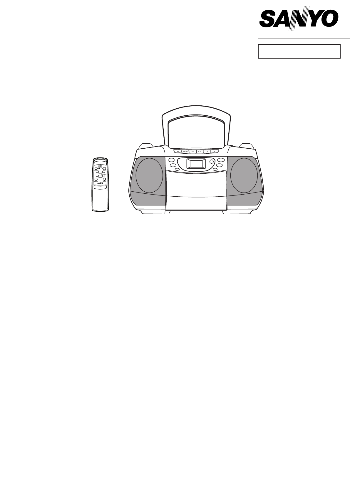
Page 1
FILE NO.
Service Manual
CD Portable Radio
Cassette Recorder
MCD-ZX250F(BL)
(XE)
MCD-ZX250F(WH)
(XE)
MCD-ZX250F (UK)
CONTENTS
Laser beam safety precaution .......................................... 1
IC Block Diagram & Description ....................................... 1,9
Tuner Adjustments ........................................................... 2
Wiring Connection ........................................................... 3
Exploded View (Cabinet & Chassis) ................................ 4
Parts List .......................................................................... 6
Schematic Diagram .......................................................... 11
Wiring Diagram ............................................................... 16
Block Diagram .................................................................. rear
PRODUCT CODE No.
164 128 02 250F(BL)/XE
164 128 13 250F(WH)/XE
164 128 01 250F/UK
REFERENCE No. SM5810611
Page 2
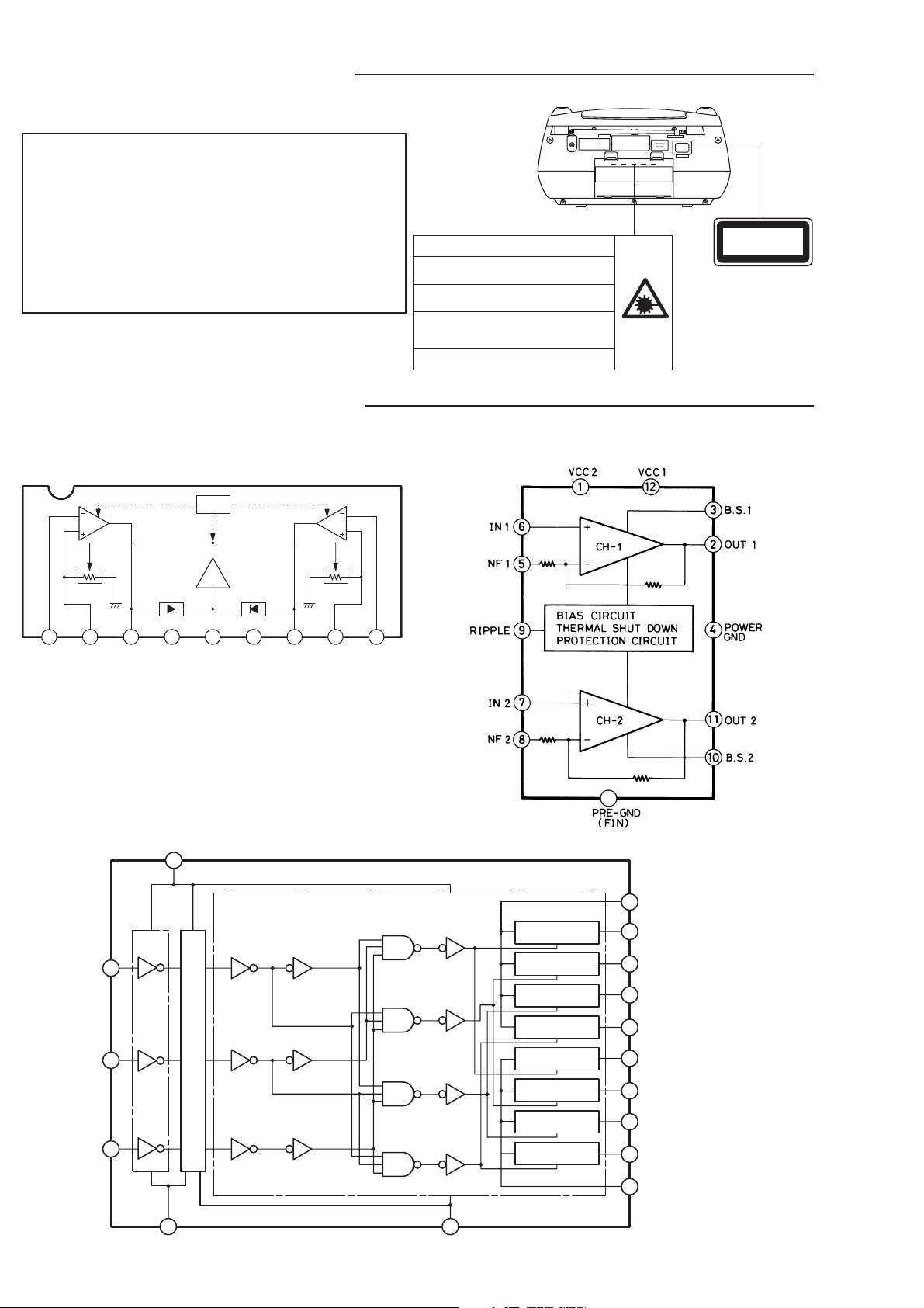
LASER BEAM SAFETY PRECAUTION
• Pickup that emits a laser beam is used on this CD section.
CAUTION :
USE OF CONTROLS OR ADJUSTMENTS OR
PERFORMANCE OF PROCEDURES OTHER
THAN THOSE SPECIFIED HEREIN MAY RESULT
IN HAZARDOUS RADIATION EXPOSURE.
LASER OUTPUT................ 0.6 mW Max. (CW)
WAVE LENGTH ................. 790 nm
CAUTION-INVISIBLE LASER RADIATION WHEN OPEN AND
INTERLOCKS DEFEATED. AVOID EXPOSURE TO BEAM.
ADVARSEL-USYNLIG LASER STRÅLING VED ÅBNING, NÅR
SIKKERHEDSAFBRYDERE ER UDE AF FUNKTION, UNDGÅ
UDS ÆTTELSE FOR STRÅLING.
VARNING-OSYNLIG LASER STRÅLNING NÄR DENNA DEL
ÄR ÖPPNAD OCH SPÄRR ÄR URKOPPLAD. STRÅLEN ÄR
FARLIG.
VORSICHT! -UNSICHTBARE LASERSTRAHLUNG TRITT
AUS, WENN DECKEL GEÖ FFNET UND ENN
SICHERHEITSVERRIEGELUNG ÜBERBRÜCKT IST. NICHT,
DEM STRAHL AUSSETZEN.
VARO !-Avattaessa ja suojalukitus ohitettaessa olet alttiina
näkymättömälle lasersäteilylle. Älä katso säteeseen.
IC BLOCK DIAGRAM & DESCRIPTION
IC201 BA3308 (Pre-Amp.) IC301 TA8227 (Power Amp.)
MUTE
ch1 ch2
CLASS 1 LASER PRODUCT
LUOKAN 1 LASERLAITE
KLASS 1 LASERAPPARAT
ALC
1
NF 1 INPUT 1 OUTPUT 1 GND ALC Vcc OUTPUT 2 INPUT 2 NF 2
23456789
IC501 TC4052(Defferential 4-Channel Multiplexer)
V
DD
16
10
A
OUT c IN
OUT c IN
OUT c IN
OUT c IN
13 X-COMMON
0X
12
1X
14
2X
15
3X
11
INH
0Y
9
B
LOGIC LEVEL CONVERTER
6
OUT c IN
OUT c IN
OUT c IN
OUT c IN
1
1Y
5
2Y
2
3Y
4
3
Y-COMMON
87
SS
V
V
EE
- 1 -
Page 3
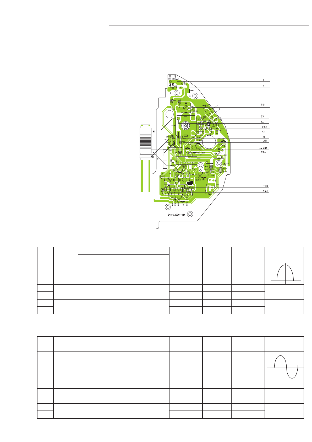
TUNER ADJUSTMENTS
Use a plastic screw driver for adjustments.
Adjust the intermediate frequency of AM and FM to the frequency of ceramic filter.
Set of unit
Supply voltage : DC 12.0V
Speaker impedance : 8 ohms
Standard output : 50 mW
Function switch : RADIO
a. Parts Location
a. AM Adjustment Band switch : AM
Step Adjustment
Adjusting Connections
Circuit lnput Output
Closed the output
terminal by sweep
1
2
3
4
5
IF generator to(19)IC101 465KHz Low T103
generator,it place
to MW ANT
Tuning Connect AM SG to Connect VTVM to 515 KHz Low end T101
coverage test loop speaker terminals. 1640 KHz High end C3
Tracking
Connect AM SG to Connect VTVM to 600 KHz 600 KHz MW ANT
test loop speaker terminals 1400 KHz 1400 KHz C4
Connect sweep
(H) 0and C112(E)
SG
Frequency
Position of VTVM
Tuning dial Oscilloscope
b. FM Adjustment Band switch : FM FM Dummy antenna : 75 ohms unbalance
Adjusting Connection position of VTVM
Step SG Frequency
Circuit Input Output tuning dial Oscilloscope
Connect sweep Connect VTVM to
1
2
3
4
5
IF generator to IC101 generator to (19)PIN 10.7MHz Low T104 andT102
IC101(22)pin (E)
Tuning Connect FM SG to Connect VTVM to 87.0 MHz Low end L102
coverage FM ANT(A) & D102(B) speaker terminals. 109.0 MHz High end C1
Tracking
Connect FM SG to Connect VTVM to 90.0 MHz 90.0 MHz L101
FM ANT(A) &D102(B) speaker terminals. 106.0 MHz 106.0 MHz C2
IC101(H) and C112(E)
Adjustment
Max.
Max.
Max.
Max.
- 2 -
Page 4
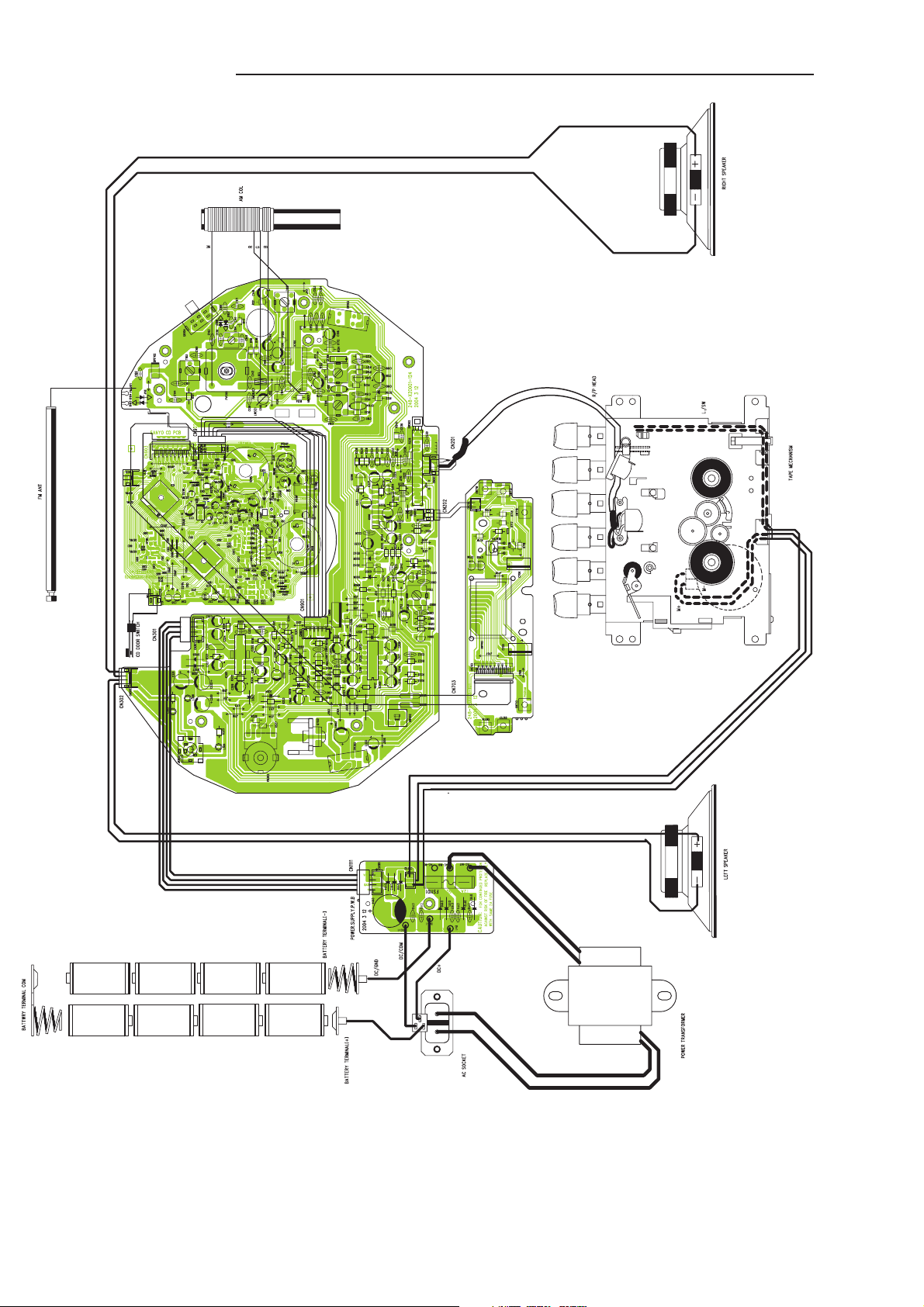
WIRING CONNECTION
This is a basic wiring connection.
- 3 -
Page 5

EXPLODED VIEW(CABINET & CHASSIS)
7A
Y20
Y1
Y19
54
52
Y18
Y17
Y16
Y15
Y13
Y12
Y11
Y10
Y9
Y8
Y7
Y5
Y4
Y3
Y1
53
12
64
63
62
61
73
72
71
51
50
49
47
48
46
43
40
42
41
39
38
37
36
35
34
28
28
31
28
30
29
33
32
25
24
23
22
21
20
19
18
17
16
15
14
13
65
11
6
5
4
3
2
1
Y2
45
44
Y14
26
27
Y6
74
47
Y18
23
Y16
43
46
Y6
24
62
49
48
51
50
52
Y17
25
28
32
26
Y7
22
15
16
12
65
5
Y1
Y3
71
11
17
18
Y2
19
20
14
33
21
Y4
Y1
3
4
13
7A
27
61
Y9
37
282828
28
Y5
38
74
34
53
35
40
36
39
Y20
Y14
Y8
29
30
31
Y13
64
44
45
63
Y12
Y10
41
42
Y15
73
2
1
72
6
: Not available as service parts.
Y11
54
Y19
- 5 -- 4 -
Page 6

PARTS LIST
PARTS LIST
PRODUCT SAFETY NOTICE
EACH PRECAUTION IN THIS MANUAL SHOULD BE FOLLOWED DURING SERVICING. COMPONENTS IDENTIFIED WITH
!!
!
THE IEC SYMBOL
CAN OF SPECIAL SIGNIFICANCE. WHEN REPLACING A COMPONENT IDENTIFIED , USE ONLY THE REPLACEMENT
PARTS DESIGNATED, OR PARTS WITH THE SAME RATINGS OF RESISTANCE, WATTAGE OR VOLTAGE THAT ARE
DESIGNATED IN THE PARTS LIST IN THIS MANUAL. LEAKAGE-CURRENT OR RESISTANCE MEASUREMENTS MUST
BE MADE TO DETERMINE THAT EXPOSED PARTS ARE ACCEPTABLY INSULATED FROM THE SUPPLY CIRCUIT BEFORE
RETURNING THE PRODUCT TO THE CUSTOMER.
CAUTION : Regular type resistors and capacitors are not listed. To know those values, refer to the schematic diagram.
PACKING & ACCESSORIES
REF.NO. PART NO. DESCRIPTION
!!
!
!!
!
CABINET & CHASSIS
REF.NO. PART NO. DESCRIPTION
1 645 069 7005 CASS DOOR((BL)/XE)(UK)
1 645 071 4740 CASS DOOR(WH/XE)
2 645 069 7197 CASS DOOR BRACKET
3 645 062 0478 CASS DOOR SPRING
4 645 069 7265 DISPLAY LENS((BL)/XE)(UK)
4 645 071 4917 DISPLAY LENS(WH/XE)
5 645 070 5304 SPEAKER GRILL LEFT((BL)/XE)(UK)
5 645 069 7364 SPEAKER GRILL LEFT(WH/XE)
6 645 070 5311 SPEAKER GRILL RIGHT
6 645 069 7371 SPEAKER GRILL RIGHT(WH/XE)
7A 645 071 4696 ASSY CABINET(WH/XE)
7A 645 069 6411 ASSY CABINET((BL)/XE)(UK)
11 645 069 7272 LCD BRACKET
12 645 069 7241 SPEAKER CLIP L
13 645 033 0407 CASS LID GEAR
15 645 069 7104 KNOB CASS PAUSE
16 645 069 7111 KNOB CASS STOP/EJECT
17 645 069 7128 KNOB CASS FFWD
18 645 069 7135 KNOB CASS REWIND
19 645 069 7142 KNOB CASS PLAY
20 645 069 7159 KNOB CASS RECORD
21 645 069 7166 RECORDING BRACKET
22 645 071 4887 DISPLAY PANEL((BL)/XE)(UK)
22 645 071 4894 DISPLAY PANEL(WH/XE)
23 645 069 7258 CD DOOR LENS((BL)/XE)(UK)
23 645 071 4900 CD DOOR LENS(WH/XE)
24 645 033 3996 CD CHUCK M
25 645 069 7210 CD DOOR
26 645 033 3972 CD MAGNET RING
27 645 033 3989 CD CHUCK A
28 645 069 7067 KNOB VOLUME,
28 645 071 4801 KNOB VOLUME,ROTARY(WH/XE)
IN THE PARTS LIST AND THE SCHEMATIC DIAGRAM DESIGNATE COMPONENTS IN WHICH SAFETY
Regular type resistors are less than 1/4W carbon type and 0 ohm chip resistors.
Regular type capacitors are less than 50V and less than 1000µF of Ceramic type and Electrolytic type.
REF.NO. PART NO. DESCRIPTION
29 645 069 7036 KNOB TUNING,
645 071 4986 GIFT BOX((BL)/XE)
645 071 4979 GIFT BOX(UK)
645 071 4993 GIFT BOX(WH/XE)
645 069 7319 INSTRUCTION MANUAL((BL)/XE)
645 071 4924 INSTRUCTION MANUAL(UK)
645 069 7319 INSTRUCTION MANUAL(WH/XE)
645 066 6063 POLY BAG,I/B
645 070 9296 POLY BAG,PWR CORD
645 069 7357 POLY BAG,UNIT
645 069 7388 POLY FOAM,
1KIT 2 PCS LEFT&RIGHT
645 069 6534 POWER CORD,VDE(XE)
645 062 5862 PWR CORD,BSI(UK)
645 071 4931 QUICK GUIDE(XE)
645 071 4955 RATING PLATE((BL)/XE)
645 071 4962 RATING PLATE(UK)
645 071 4955 RATING PLATE(WH/XE)
645 071 4702 REMOTR CONTROL,
RC06-1020S3-490
((BL)/XE)(UK)
29 645 071 4771 KNOB TUNING,ROTARY(WH/XE)
30 645 069 7180 TUNING KNOB GEAR
31 645 069 7074 KNOB BAND,SLIDE((BL)/XE)(UK)
31 645 071 4818 KNOB BAND,SLIDE(WH/XE)
32 645 069 7081 KNOB FUNCTION,
32 645 071 4825 KNOB FUNCTION,PUSH(WH/XE)
33 645 069 7050 KNOB BASS,PUSH((BL)/XE)(UK)
33 645 071 4795 KNOB BASS,PUSH(WH/XE)
34 645 069 7043 DIAL LENS((BL)/XE)(UK)
34 645 071 4788 DIAL LENS(WH/XE)
35 645 071 4856 CABINE TOP((BL)/XE)(UK)
35 645 071 4863 CABINE TOP(WH/XE)
36 645 069 6961 CD MECKANISM COVER
37 645 069 6893 CD DECK MECHANISM,DA11MM
38 645 033 3446 RUBBER SILICON,FOR CD DECK
39 645 033 0407 CD LID GEAR
40 645 070 9326 CD DOOR LOCK
41 645 071 4832 POINTER((BL)/XE)(WH/XE)
41 645 071 4849 POINTER(UK)
42 645 069 6992 POINTER BRACKET
43 645 069 7029 HANDLE((BL)/XE)(UK)
43 645 071 4764 HANDLE(WH/XE)
45 645 033 0391 AC SKT COVER
46 645 069 6985 CABINET BACK((BL)/XE)(UK)
46 645 071 4733 CABINET BACK(WH/XE)
48 645 069 7012 BATTERY DOOR((BL)/XE)(UK)
48 645 071 4757 BATTERY DOOR(WH/XE)
49 645 070 9319 BATTERY SPRING+
50 645 033 0926 BATT SPRING(+)
52 645 070 9302 BATTERY SPRING51 645 070 9319 BATTERY SPRING+
53 645 042 0351 CD DOOR SPRING
54 645 069 7173 TUNING DRUM
ROTARY((BL)/XE)(UK)
PUSH((BL)/XE)(UK)
FIXING PARTS
REF.NO. PART NO. DESCRIPTION
Y1 645 069 6794 SCREW 3X10,SPEAKER CLIP R
Y2 645 069 6794 SCREW 3X10,CASS DOOR GEAR
Y3 645 023 6594 SCREW ST 3X8,CONTROL PCB-PB
Y4 645 069 6787 SCREW 3X10,
TOP CAB TO FRONT CAB
AC SKT COVER TO AC SKT-SST
POWER TRANSFORMER-SST
RECTIFER BOARD-PB
ROTARY((BL)/XE)(UK)
Y5 645 069 6794 SCREW 3X10,SPEAKER CLIP L
Y6 645 069 6770 SCREW 2.6X8,CD DECK
Y7 645 062 1086 SCR 2X5,CD DOOR,
Y8 645 069 6787 SCREW 3X10,CASS DECK
Y9 645 069 6824 SCREW 2X6,LEAF SWITCH
Y10 645 033 0247 SCR 2.6X8,CD DOOR GEAR
Y11 645 023 6594 SCREW ST 3X8,MAIN PCB-PB
Y12 645 027 1144 SCR 2.8X12,
Y14 645 027 1182 SCR 3X20,
Y15 645 023 6594 SCREW ST 3X8,
REF.NO. PART NO. DESCRIPTION
Y16 645 023 6617 SCREW ST 3X10,
Y17 645 070 4819 SCREW 3X25,
Y18 645 027 1236 SCR 3X8,ROD ANTENNA-SM
Y19 645 069 6831 SCREW 2.6X6,TUNING DRUM
Y20 645 069 6770 SCREW 2.6X8,CD DECK
TOP CAB TO BACK CAB-PB
BACK CAB TO FRONT CAB
ELECTRICAL-PARTS
REF.NO. PART NO. DESCRIPTION
47 645 070 9043 ROD ANTENNA
61 645 069 6657 LEAF SWITCH,CD LID SW,LS-053-02
62
63 645 032 9760 AC SOCKET S-1-1225,SW1110,230V
65 645 069 6558 SPEAKER
!!
!
645 071 4719 POWER TRANSFORMER
645 069 6855 6P HSG,
645 069 6763 FFC CABLE 18P,
645 054 0707 HSG 3P,
645 033 3606 FERRITE BEAD,
645 055 7095 FERRITE BEAD,
645 033 3606 FERRITE BEAD,
645 055 7255 16P FFC CABLE,
645 069 6749 2P HSG,
645 069 6756 2P HSG,
645 069 6732 4P HSG,MAIN CN 302 TO SPEAKER
645 069 6725 4P HSG,
645 069 6848 4P HSG,
MAIN CN901 TO CD BD CN90,2.0MM
CTL CN703 TO CD DECK,K 1MM
RECTI CN1112 TO CASS DEC
CN901 TO CN902 6P CROSS
X’FORMER INPUT W CROSS 2
X’FORMER OUTPUT W CROSS
CD BD CN901 TO CD DECK
CD BD CN904 TO CD LEAF S
MAIN CN202 TO CTL CN702
MAIN CN201 TO CASS DECK
RECTI CN1111 TO MAIN CN3
COTORL P.W.BOARD ASSY
REF.NO. PART NO. DESCRIPTION
71 614 331 9757 ASSY,PWB,CONTROL
C0703 645 034 9669 ELECT CAP 100 UF/10V
CN703 645 069 6701 FFC HEADER 18P,18P 1MM
Q0701 645 023 6129 TR 9014C
Q0702 645 023 6129 TR 9014C
REM701 645 033 3477 DIODE RPM-6938-V4
SW701 645 069 6640 SWITCH TACT,MEMORY
SW702 645 069 6640 SWITCH TACT,SKIP+
SW703 645 069 6640 SWITCH TACT,STOP
SW704 645 069 6640 SWITCH TACT,PALY
SW705 645 069 6640 SWITCH TACT,SKIPSW706 645 069 6640 SWITCH TACT,REPEAT
645 069 7272 LCD BRACKET
645 069 6671 LCD DISPLAY,9P 30X20.5MM
MAIN P.W.BOARD ASSY
REF.NO. PART NO. DESCRIPTION
72 614 331 2475 ASSY,PWB,MAIN(Only initial)
BPF101 645 055 6937 BAND PASS FILTER,88-108MHZ
C0117 403 057 8300 POLYESTER 0.012U M 50V
C0120 403 057 8300 POLYESTER 0.012U M 50V
C0201 403 059 4409 POLYESTER 2200P M 50V
C0208 403 061 9003 POLYESTER 4700P M 50V
C0209 403 059 4409 POLYESTER 2200P M 50V
C0210 403 060 8908 POLYESTER 0.033U M 50V
C0211 403 061 9003 POLYESTER 4700P M 50V
C0213 403 060 8908 POLYESTER 0.033U M 50V
C0308 403 057 3800 POLYESTER 0.1U M 50V
C0311 403 057 3800 POLYESTER 0.1U M 50V
C0513 403 058 6008 POLYESTER 0.15U M 50V
C0514 403 058 6008 POLYESTER 0.15U M 50V
C0802 403 061 9003 POLYESTER 4700P M 50V
C0804 403 059 6908 POLYESTER 0.022U M 50V
C0806 403 057 1202 POLYESTER 0.01U M 50V
C0959 403 059 4409 POLYESTER 2200P M 50V
C0960 403 059 4409 POLYESTER 2200P M 50V
CF101 645 062 0768 CERAMIC FILTER,10.7MS3
CF102 645 062 0768 CERAMIC FILTER,10.7MS3
CF103 645 044 6955 CERAMIC FILTER,465 B KHZ 3PIN
CN201 645 069 6718 HEADER 4P,4P 2MM
CN302 645 069 6718 HEADER 4P,4P 2MM
D0101 645 023 6099 DIODE 1N-4148
D0102 645 023 6099 DIODE 1N-4148
D0105 645 033 3842 DIODE FV1043
D0201 645 023 6099 DIODE 1N-4148
D0202 645 023 6099 DIODE 1N-4148
D0203 645 023 6099 DIODE 1N-4148
D0204 645 023 6099 DIODE 1N-4148
D0301 645 023 6112 RECTIFIER 1N-4001
D0302 645 023 6099 DIODE 1N-4148
D0501 645 023 6099 DIODE 1N-4148
D0502 645 023 6099 DIODE 1N-4148
D0908 645 023 6099 DIODE 1N-4148
D0909 645 023 6099 DIODE 1N-4148
D0910 645 023 6099 DIODE 1N-4148
D1117 645 023 6112 RECTIFIER 1N-4001
D1118 645 023 6112 RECTIFIER 1N-4001
DZ101 645 023 6105 ZENER DIODE-4.7V,1/2W
IC101 645 041 9973 IC LA1824
IC201 645 032 9906 IC BA3308
IC301 645 034 9980 IC TA-8227P TOSHIB
IC501 645 061 9908 IC TC4052BP
JK601 645 061 9991 ST EARPHONE JACK
L0101 645 023 6297 VHF COIL-T3.5,4.5X0.7MM
L0102 645 024 1031 FTZ COIL,
BH-81228712-21/T8,7MM,0.6MM
PVC101 645 026 6676 PVC,DF-443DF2-A04
Q0101 645 027 3797 TR 9018H
Q0201 645 023 6129 TR 9014C
Q0202 645 023 6129 TR 9014C
Q0203 645 023 6129 TR 9014C
Q0301 645 023 6129 TR 9014C
Q0302 645 023 6129 TR 9014C
Q0801 645 023 6129 TR 9014C
Q0802 645 027 0420 TR 8050C
Q0905 645 023 6129 TR 9014C
Q0906 645 023 6129 TR 9014C
Q1101 645 066 5790 IC KA7808
SW101 645 024 1048 SW SLIDE SK22F03G6,SK22F03G6
SW102 645 069 6664 SWITCH SILDE,SS22E01G6,2P2T
SW201 645 035 0023 RECORDING SW. PS-62D,
PS-62D01-S,218-662205-007
SW301 645 042 0054 SW SLIDE,SS23E01G6,2P2T
SW501 645 042 0030 SW PUSH,PS-8.5X8.5-180G
T0101 645 026 6669 AM OSC,OSC 1010-RED,10MM
T0102 645 027 0437 FM IFT,IF 0070-ORANGE,10MM
T0103 645 033 3866 AM COIL,IF 2070,YELLOW,10MM
T0104 645 027 0444 FM IFT,IF 0380-PINK,10MM
- 7 -- 6 -
Page 7

1
234
5
678910 11 12
24
23 22 21
20
19 18 17
16
15 14 13
FM
RF
AM
RF
AM
MIX
FM
MIX
FM
OSC
AM
OSCREG Vcc1
Vcc2GND2
GND1
DECODER
PHASE
COMP
PILOT
DET
TRIG ST-SW VCO
DET
DET
AM-IF
S-METER
FM-IF
AGC
FF FF FF
ST
LED
TUN
LED
PARTS LIST
IC BLOCK DIAGRAM & DESCRIPTION
REF.NO. PART NO. DESCRIPTION
T0801 645 027 0307 BIAS COIL,
AC BIAS 3630-BLACK,10MM
VR301 645 042 0085 ROTARY VR,50K
645 042 0344 CONTACT PIN,FM ANT,1MM
645 061 9946 1P HSG,FM ANT
645 042 0337 HEAT SINK,FOR MAIN BD.IC301,
41X22X0.4MM
645 069 6404 ASSY BAR ANT
POWER SUPPLY P.W.BOARD ASSY
REF.NO. PART NO. DESCRIPTION
73 614 331 2499 ASSY,PWB,RECTIFIER(Only initial)
C1114 403 135 5702 ELECT 4700U M 25V,HW SERIES
D1110 645 023 6112 RECTIFIER 1N-4001
D1111 645 023 6112 RECTIFIER 1N-4001
D1112 645 023 6112 RECTIFIER 1N-4001
D1113 645 023 6112 RECTIFIER 1N-4001
D1114 645 023 6112 RECTIFIER 1N-4001
D1115 645 023 6112 RECTIFIER 1N-4001
D1116 645 023 6112 RECTIFIER 1N-4001
FS1101 645 054 0639 FUSE GLASS TUBE,2A 250V
CN1111 645 027 0611 WAFER 4P,2.5MM,PITCH
CN1112 645 033 3682 HEADER 3PINS,JST,2MM PITCH
645 035 0511 FUSE HOLDER MW1010K,
FOR FS1101,406-050090-000
645 027 1298 EYELET
CD P.W.BOARD ASSY
REF.NO. PART NO. DESCRIPTION
74 614 331 2505 ASSY,PWB,CD(Only initial)
CN901 645 069 6688 HEADER FFC 16P,16P 1MM
CN902 645 051 6542 6P HEADER,2MM
CN903 645 069 6695 HEADER FFC 18P,18P 1MM
CN904 645 051 6511 2P HEADER,2MM
D0901 645 023 6099 DIODE 1N-4148
D0902 645 023 6099 DIODE 1N-4148
IC901 645 055 8436 IC LA9242M
IC902 645 069 6633 IC LC78601RE
IC903 645 069 6879 IC LA6541D
L0901 645 042 0108 CHOKE COIL 26UH,26UH
L0902 645 069 6886 INDUCTOR 2.7UH,2.7UH CHIP 0805
L0903 645 069 6886 INDUCTOR 2.7UH,2.7UH CHIP 0805
L0904 645 069 6886 INDUCTOR 2.7UH,2.7UH CHIP 0805
L0905 645 069 6886 INDUCTOR 2.7UH,2.7UH CHIP 0805
Q0901 645 061 8246 TR 2SA608NFNPAAT
Q0902 645 033 3514 TR 2SB764D
Q0903 645 069 6862 TRANSISTOR 2SA1342
Q0904 645 069 6862 TRANSISTOR 2SA1342
X0901 645 061 9915 RESONATOR 16.9344MHZ,
16.9344MHZ
645 042 0320 HEAT SINK,FOR CD BD IC903,
36X23X1.2MM
IC903 LA6541 (CD Driver) IC101 LA1824 (Tuner)
Vcc Vref VIN4 VG4 Vo8 Vo7 GND Vo6 Vo5 VG3 VIN3 CD RES
11k Ω 11k Ω
Level
Sift
Level
Sift
123 456 789
Vcc Mute VIN1 VG1 Vo1 Vo2 GND Vo3 Vo4 VG2 VIN2 Reg OUT Reg IN
Driver
Driver
Vcc
BTL
BTL
BTL
Driver
BTL
Driver
Level
Sift
Level
Sift
11k Ω11k Ω
10 11 12
131415161718192021222324
RESET
Regulator
IC901 LA9242M (Servo)
-
FE
LF2
59
2221
FE-
VR
VCC2
REF1
56
57
58
REF
U-COM
INTER FACE
SPINDLE SERVO
25
23
24
SP
NC
AGN D
SPG
DRF
CE
53
CL
DAT
525150
FSS
55
54
SLED SERVO
-
+
27
28
26
SP-
SPD
SLEQ
VCC1
64
FIN2
1
FIN1
2
I/V
E
3
F
4
5
TB
TE-
6
TE
7
TESI
8
9
SCI
10
TH
11
TA
12
TD-
TD
JP
TO
FD
13
14
15
16
-
+
PIN FUNCTION
LDD
LDS
62
63
APC
TE
+
-
T.SERVO & T.LOGIC
PH1
BH1
60
61
RF DET
VCA
VCABAL
F.SERVO & F.LOGIC
+
+
-
17
FD -
-
18
FA
+
19
20
FA-
CLK
RF Amp
29
SLD
SLC
+
-
DEF
49
48
NC
47
TBC
46
FSC
45
DGND
44
-
+
-
+
3130
SL-
SL+
SLI
43
SLC
42
RFS-
41
RFSM
40
CV+
39
CV-
38
SLOF
37
HFL
36
TES
35
TOFF
34
TGL
33
JP+
32
JP-
TAPE DECK MECHANISM
REF.NO. PART NO. DESCRIPTION
14 645 050 1814 CASS DECK MECHANISM,
P21VB-A83-2L1F4
645 050 2101 ASSY,MOTOR
645 068 7976 ASSY,PINCH ROLLER
645 050 1784 MAIN BELT
645 050 1395 RF BELT,34 X 1 X 1
645 018 0637 R/P HEAD,TC-915
645 030 6839 E HEAD
1 FIN2
2 FIN1
3 E
4 F
5 TB
6 TE-
7 TE
8 TESI
9 SCI
10
TH
11 TA
12 TD-
13 TD
14 JP
15 TO
16 FD
17 FD-
18 FA
19 FA-
20
FE
21 FE-
22 AGND
23 NC
24 SP
25 SPG
26 SP-
27 SPD
28 SLEQ
29 SLD
30 SL-
31 SL+
32 JP-
33 JP+
34 TGL
35 TOFF
36 TES
37 HFL
38 SLOF
39 CV-
40 CV+
- 9 -- 8 -
41 RFSM
42 RFS-
43 SLC
44 SLI
45 DGND
46 FSC
47 TBC
48 NC
49 DEF
50 CLK
51 CL
52 DAT
53 CE
54 DRF
55 FSS
56 Vcc2
57 REF1
58 VR
59 Lf2
60 Ph1
61 BH1
62 LDD
63 LDS
64
Vcc1
Page 8

IC BLOCK DIAGRAM & DESCRIPTION
IC902 IC78601RE (ANALOG SIGNAL PROCESSOR)
SCHEMATIC DIAGRAM (TUNER)
No. Pin Name
1 DEF1
2 3V / *5V
3 PDO
4 VVss
5 ISET
6 VVdd
7FR
8 Vss
9 EFMO
10 EFMIN
11 TMOD
12 CLV
13 HFL
14 TES
15 TOFF
16 TGL
17 JP
18 LASER
19 FSTA
20 EFBAL
21 SP8
22 Vdd
23 FSEQ
24 PCK
25 SLOF
26 SLED+
27 SLED-
28 PUIN
29 DOUT
30 N C
31 *SEG8
32 *SEG7
Function
It is junction in unused time, 0 V defect detecting signal (DEF) input
terminal
It is 5 V use 3 V use, L H power supply voltage selection input terminal.
The phase comparison output terminal for outside VCO control(PLL
control)
Earth terminal for internal organs VCO control , connecting it to 0 V by
all means
Resistance connection terminal for electric current adjustment of PDO
output
Power supply terminal for internal VCO control
VCO frequency range adjustment control
Digital series earth terminal. Being connected to 0 V by all means.
EFM signal output terminal.(Slice level control )
EFM signal input terminal.(Slice level control )
Input terminal for a test. (Being connected to 0 V by all means)
The output terminal for disk motor control. 3 value output
Truck detecting signal input terminal.
Tracking error signal input terminal.
Tracking OFF output terminal
The output terminal for tracking gain change. (Go up gain with L)
The output terminal for tracking jump control. (3 value output)
Laser control terminal. (The pull-down resistor internal )
The FS TA control terminal. (The pull-down resistor internal )
EFBAL control terminal. (The pull-down resistor internal )
SP 8 control terminal. (The pull-down resistor internal )
Digital series power supply terminal
The synchronising signal search output terminal. When synchronising
signal of inside creation agreed with the synchronising signal which
detected it from EFM signal, it become "H"
Clock monitor terminal for EFM data reproduction. ( Limited at the time
of test mode but)
Thread OFF control output terminal
The thread field output terminal
The thread field output terminal
Limit switch sensing input terminal. (The pull-up resister internal )
Digital OUT output terminal. (EIAJ format)
NC (Being open)
The segment output (8) terminal. (The pull-up resister internal )
The segment output (7) terminal. (The pull-up resister internal )
No. PIN NAME Function
33 *SEG6 The segment output (6) terminal. (The pull-up resister internal )
34 *SEG5 The segment output (5) terminal. (The pull-up resister internal )
35 *SEG4 The segment output (4) terminal. (The pull-up resister internal )
36 *SEG3 The segment output (3) terminal. (The pull-up resister internal )
37 *SEG2 The segment output (2) terminal. (The pull-up resister internal )
38 *SEG1 The segment output (1) terminal. (The pull-up resister internal )
39 Vcc Digital series earth terminal. (It is connection in 0 V by all means)
40 NC NC
41 *DIG2 The common drive output (2) terminal.The pull-up resister internal
42 *DIG1 The common drive output (1) terminal.The pull-up resister internal
43 *PROG
44 *KEYIN Key matrix input terminal. (The pull-up resister internal )
45 N C NC (Being open)
46 N C NC (Being open)
47 *RANDOM Random mode display output terminal
48 RMTSL3 The wireless remote controller identification input (3) terminal
49 EFLG C1 , C2 , 1 fold , 2fold Correction monitor
50 FSX
51 *AMUTE audio , Mute output signal
52 REMOTE Wireless remote controller signal input terminal
53 RMTSL2 Wireless remote controller identification input(2) terminal
54 LCHO D/A , L channel output terminal
55 L/R Vdd D/A control power source terminal
56 L/RVss D/A control earth terminal. (It is connection in 0 V by all means)
57 RCHO D/A, R channel output terminal
58 CLOSE Closing switch sensing input terminal. The pull-up resister internal
59 RMTSL1
60 Xout Connection terminal of 16.9344 MHz crystal OSC
61 Xin Connection terminal of 16.9344 MHz crystal OSC
62 XVdd Power supply terminal for crystal OSC
63 *RES Reset input terminal
64 DRF DRF input terminal
Program movement monitor output terminal. (The pull-up resister
internal )
7.35KHz synchronizing signal output terminal which did dividing from
OSC. As a condition, Limited at the time of test mode
Wireless remote controller identification input(1) terminal. (The pull-up
resister internal )
This is a basic schematic diagram.
- 11 -- 10 -
Page 9

SCHEMATIC DIAGRAM (MAIN)
This is a basic schematic diagram.
- 13 -- 12 -
Page 10

SCHEMATIC DIAGRAM (CD)
This is a basic schematic diagram.
- 15 -- 14 -
Page 11

WIRING DIAGRAM (MAIN , POWER SUPPLY & CONTROL)
This is a basic wiring diagram.
POWER SUPPLY
MAIN
CONTROL
- 17 -- 16 -
Page 12

WIRING DIAGRAM (CD )
BLOCK DIAGRAM
This is a basic wiring diagram.
This is a basic block diagram.
Jun./ '04 BB Printed in Japan
SANYO Electric Co., Ltd.
Osaka, Japan
- 19 -- 18 -
 Loading...