

Page 1
FILE NO.
Service Manual
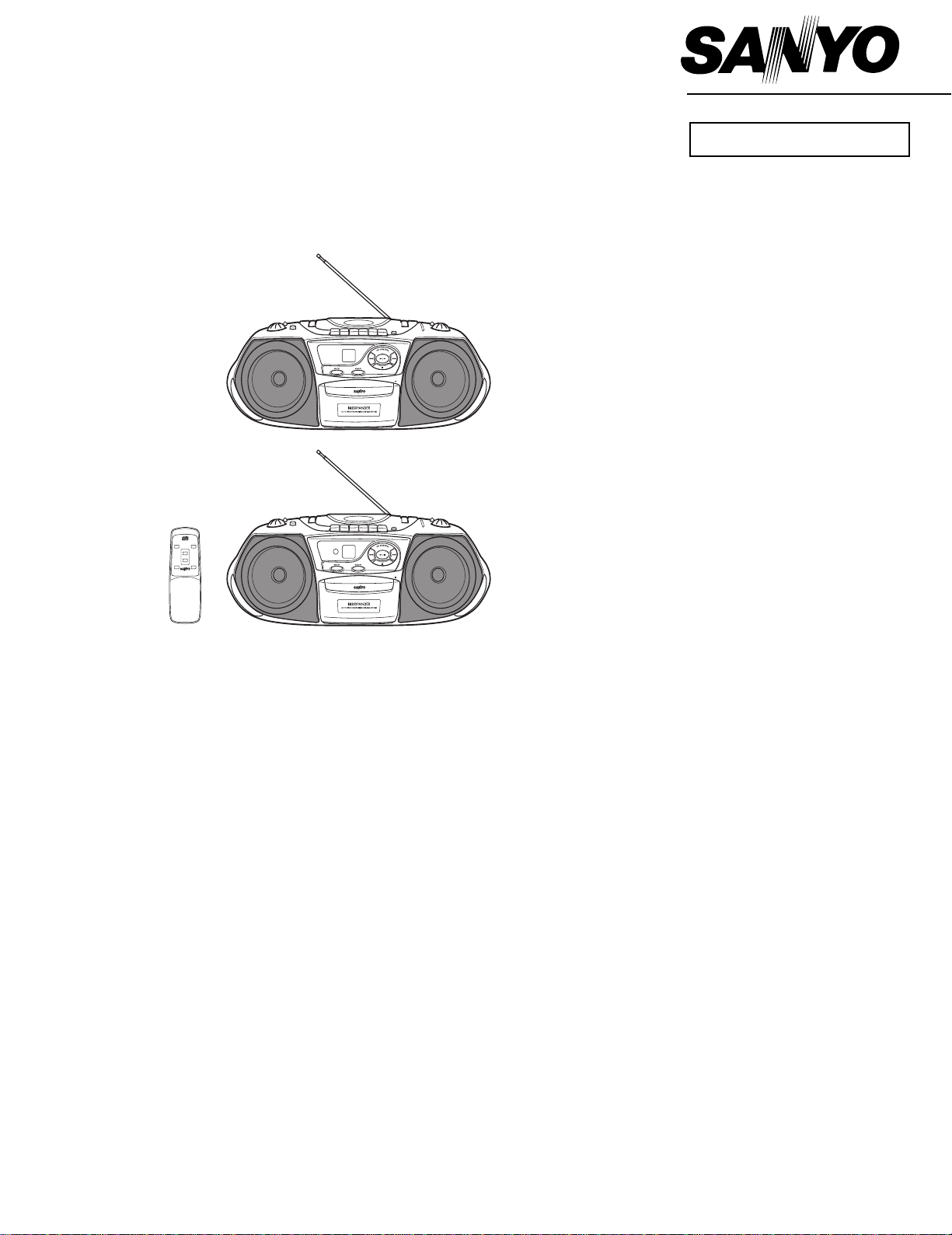
CD Portable Radio
Cassette Recorder
MCD-Z128 Series
CWM-240
MCD-Z130 Series
SPECIFICATIONS
(CASSETTE SECTION)
Recording System.................4-track, 2-channel stereo
Erasing System ..................... Magnet erase
Tape speed ...........................4.75 cm/sec.
Fast forward and
Rewind time .................... Approx. 110 sec. (C-60 tape)
Frequency range .................. 80 - 12,000 Hz (Normal tape)
(CD PLAYER SECTION)
Channels ............................... 2 channels stereo
Wow & Flutter........................Below measurable limits
Sampling frequency .............. 44.1 kHz
Quantization .......................... 16 bits linear/ch
Pickup light source ................ Semi-conductor laser
Pickup wave length ...............790 nm
Laser output ..........................Continuous wave max. 0.6 mW
CWM-240 (MX)
MCD-Z128 series
MCD-Z130 series
PRODUCT CODE No.
164 073 07 CWM-240/MX
164 073 02 MCD-Z128F/XE
164 073 06 MCD-Z128F/AU
164 073 00 MCD-Z130F/XE
164 073 01 MCD-Z130/CA
164 073 03 MCD-Z130F/AU
164 073 04 MCD-Z130F/PA
164 073 30 MCD-Z130L/UK
(RADIO SECTION)
Tuning range ......................... FM : 87.5 - 108 MHz
AM : 526.5 - 1,606.5 kHz
LM : 148.5 - 283.4 kHz(130L Only)
(GENERAL SECTION)
Power output ......................... 2W/ch (DC max)
Speaker.................................10 cm x 2
Terminal impedance .............PHONES : 32 ohms
Power source ........................AC : 120V, 60Hz (MX,CA)
: 230V, 50Hz (XE,UK)
: 230-240V, 50Hz (AU)
: 110-120/220-240V, 50/60Hz (PA)
DC : 12 V (8 "R20/D" batteries)
Dimensions ........................... 472 (W) x 158 (H) x 252 (D) mm
Weight (approx.)....................3.0 kg (Not including batteries)
Specifications subject to change without notice.
REFERENCE No. SM5810232
Page 2
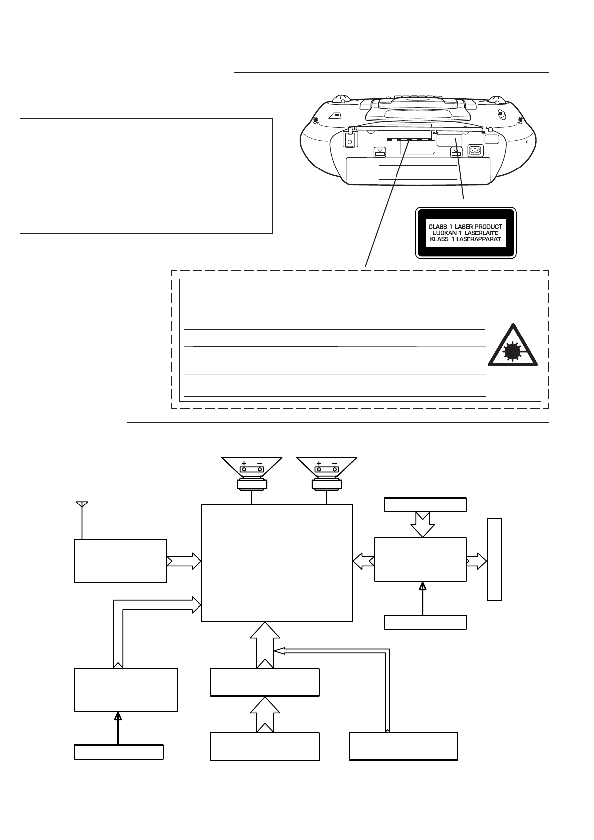
LASER BEAM SAFETY PRECAUTION
• Pickup that emits a laser beam is used on this CD section.
CAUTION :
USE OF CONTROLS OR ADJUSTMENTS OR
PERFORMANCE OF PROCEDURES OTHER
THAN THOSE SPECIFIED HEREIN MAY RESULT
IN HAZARDOUS RADIATION EXPOSURE.
LASER OUTPUT................ 0.6 mW Max. (CW)
WAVE LENGTH ................. 790 nm
(AU,XE,PA)
CAUTION – INVISIBLE LASER RADIATION WHEN OPEN AND
INTERLOCKS DEFEATED. AVOID EXPOSURE TO BEAM.
ADVARSEL – USYNLIG LASER STRÅLING VED ÅBNING, NÅR
SIKKERHEDSAFBRYDERE ER UDE AF FUNKTION, UNDGÅ UDS ÆTTELSE
FOR STRÅLING.
VARNING – OSYNLIG LASER STRÅLNING NÄR DENNA DEL ÄR ÖPPNAD
OCH SPÄRR ÄR URKOPPLAD. STRÅLEN ÄR FARLIG.
VORSICHT – UNSICHTBARE LASERSTRAHLUNG TRITT AUS, WENN
DECKEL GEÖFFNET UND WENN SICHERHEITSVERRIEGELUNG
ÜBERBRÜCKT IST. NICHT, DEM STRAHL AUSSETZEN.
VARO – AVATTAESSA JA SUOJALUKITUS OHITETTAESSA OLET ALTTIINA
NÄKYMÄTTÖMÄLLE LASERSÄTEILYLLE. ÄLÄ KATSO SÄTEESEEN.
BLOCK DIAGRAM
FM ANT
AM/FM RADIO
IC LA1824
CASSETTE SYSTEM
IC TA2068H
8 ohm SPEAKER X 2
RECTIFIER BOARD
MAIN BOARD
FUNCTION SELECT
VOLUME CONTROL
POWER AMP
IC LA4627
CD CONTROL
CD SYSTEM
CD LED DISPLAY
CD DECK
CASSETTE DECK
TRANSFORMER
- 1 -
DC SUPPLER
Page 3
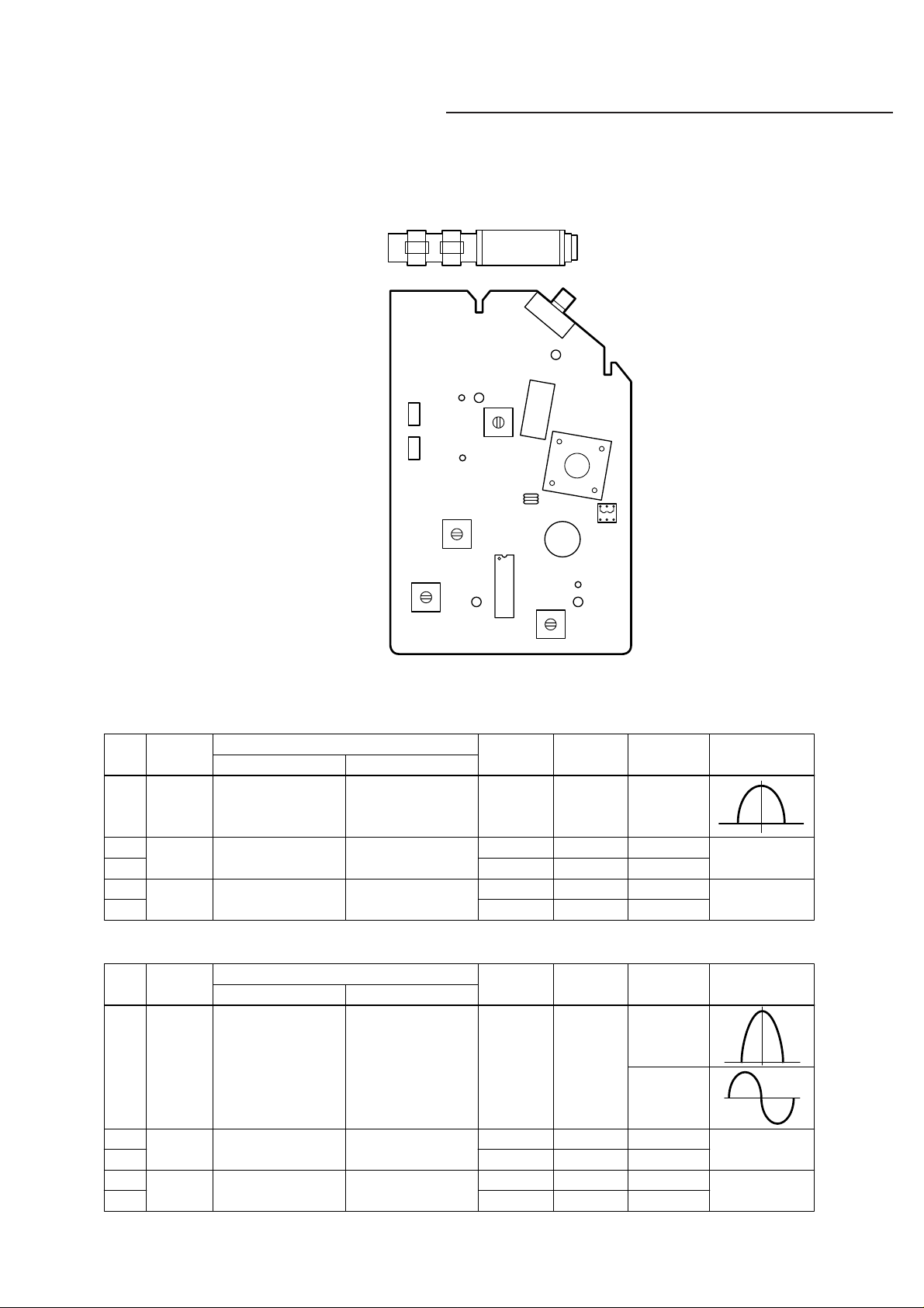
TUNER ADJUSTMENTS (All except Z130L)
Use a plastic screw driver for adjustments.
Adjust the intermediate frequency of AM and FM to the frequency of ceramic filter.
Set of unit
Supply voltage : DC 12.0V
Speaker impedance : 8 ohms
Standard output : 50 mW
Function switch : RADIO
AM COIL
248-130801-124
T104
a. AM Adjustment Band switch : MW
Step
1
2
3
4
5
Adjusting
Circuit
IF
Tuning
coverage
Tracking
Closed the output
terminal by sweep
generator,it place
to MW ANT
Connect AM SG to
test loop
Connect AM SG to
test loop
Input
Connections
Output
Connect sweep
generator to (19)
IC101(H) 0and C114(E)
Connect VTVM to
speaker terminals.
Connect VTVM to
speaker terminals.
T103
T101
SW102
SW101
L104
IC101
SG
Frequency
465 KHz
515 KHz
1640 KHz
600 KHz
1400 KHz
C3
C2
T105
Position of
Tuning dial
Low end
High end
600 KHz
1400 KHz
PUC
C1
Low
C4
L105
Adjustment
T104
T101
C3
MW AMT
C4
VTVM
Oscilloscope
Max.
Max.
b. FM Adjustment Band switch : FM FM Dummy antenna : 75 ohms unbalance
Step
1
Adjusting
Circuit
IF
Connections
Input
Connect sweep
generator to
IC101(1)pin (H) &
IC101(2)pin (E)
Output
Connect VTVM to
generator to (19)
IC101(H) and C104(E)
SG
Frequency
10.7 MHz
Position of
Tuning dial
Low
Adjustment
T103
Oscilloscope
T105
2
3
4
5
Tuning
coverage
Tracking
Connect FM SG to
JP105(H) & D102(E)
Connect FM SG to
JP105(H) & D102(E)
Connect VTVM to
speaker terminals.
Connect VTVM to
speaker terminals.
87.30 MHz
108.75 MHz
90.0 MHz
106.0 KMz
Low end
High end
90.0 MHz
106.0 MHz
L105
C1
L104
C2
- 2 -
VTVM
Max.
Max.
Page 4
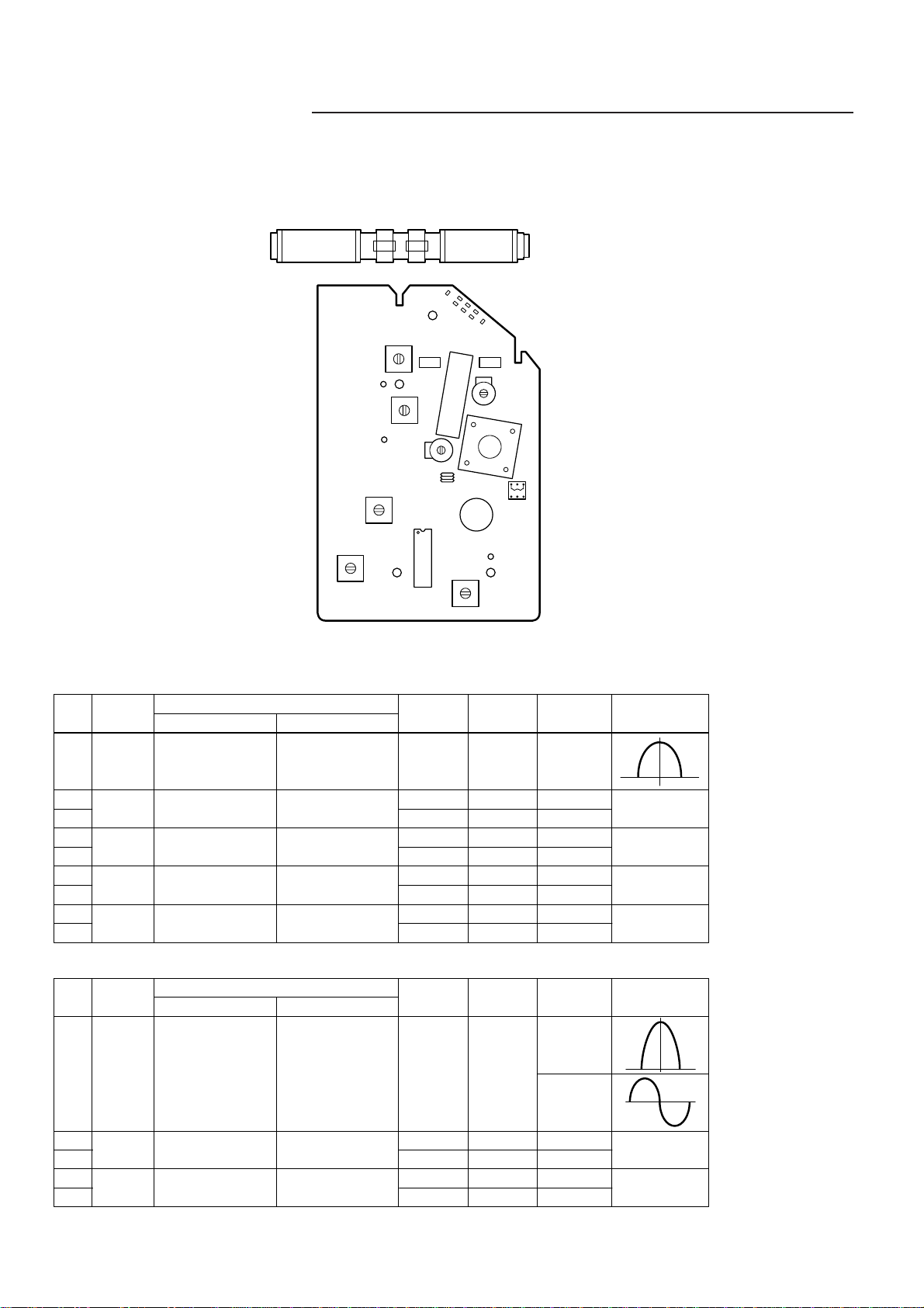
TUNER ADJUSTMENTS (Z130L)
Use a plastic screw driver for adjustments.
Adjust the intermediate frequency of AM and FM to the frequency of ceramic filter.
Set of unit
Supply voltage : DC 12.0V
Speaker impedance : 8 ohms
Standard output : 50 mW
Function switch : RADIO
MW COILLW COIL
248-130901-124
T104
a. AM Adjustment Band switch : MW
Step
1
2
3
4
5
6
7
8
9
Adjusting
Circuit
IF
Tuning
coverage
Tracking
Tuning
coverage
Tracking
Closed the output
terminal by sweep
generator,it place
to MW ANT
Connect AM SG to
test loop
Connect AM SG to
test loop
Connect AM SG to
test loop
Connect AM SG to
test loop
Input
Connections
Output
Connect sweep
generator to (19)
IC101(H) 0and C114(E)
Connect VTVM to
speaker terminals.
Connect VTVM to
speaker terminals.
Connect VTVM to
speaker terminals.
Connect VTVM to
speaker terminals.
T102
T101
T103
CT106
L104
IC101
Frequency
465 KHz
515 KHz
1640 KHz
600 KHz
1400 KHz
140 KHz
290 KHz
160 KHz
250 KHz
SW102
SG
SW101
C2
T105
Position of
Tuning dial
CT102
PUC
C4
C3
C1
L105
Low
Low end
High end
600 KHz
1400 KHz
Low end
High end
600 KHz
1400 KHz
Adjustment
T104
T102
C3
MW COIL
C4
T101
CT106
LW COIL
CT105
VTVM
Oscilloscope
Max.
Max.
Max.
Max.
b. FM Adjustment Band switch : FM FM Dummy antenna : 75 ohms unbalance
Step
1
Adjusting
Circuit
IF
Connections
Input
Connect sweep
generator to
IC101(1)pin (H) &
IC101(2)pin (E)
Output
Connect VTVM to
generator to (19)
IC101(H) and C104(E)
SG
Frequency
10.7 MHz
Position of
Tuning dial
Low
Adjustment
T103
Oscilloscope
T105
2
3
4
5
Tuning
coverage
Tracking
Connect FM SG to
JP105(H) & D102(E)
Connect FM SG to
JP105(H) & D102(E)
Connect VTVM to
speaker terminals.
Connect VTVM to
speaker terminals.
87.30 MHz
108.75 MHz
90.0 MHz
106.0 MHz
Low end
High end
90.0 MHz
106.0 MHz
L105
C1
L104
C2
- 3 -
VTVM
Max.
Max.
Page 5
TAPE DECK ADJUSTMENTS
1. HEAD REPLACEMENT
• After replacement, demagnetize the heads by using a degausser.
• Be sure to clean the heads before attempting to make any adjustments.
• All wiring should be returned to the original position after work is completed.
2. HEAD AZIMUTH ADJUSTMENT
(1) Load the test tape(VTT-703, etc., 10 kHz) for azimuth
adjustment.
(2) Press the PLAY button.
(3) Use a cross-tip screwdriver to turn the screw for azimuth
adjustment so that the left and right output are maximized.
(4) Press the STOP button.
(5) After completion of the adjustment, use thread lock(TB-1401B)
to secure the azimuth-adjustment screw.
3. AC BIAS FREQUENCY ADJUSTMENTS.
(1) Connect counter to T201(BS).
(2)R/P switch in recording state.
(3) Adjusting T801 use a plastic screw, AC bias frequency : 50 kHz
4. MOTOR SPEED ADJUSTMENT
(1) Insert the test tape(TCC-119, etc., 3,000 Hz).
(2) Press the PLAY button.
(3) Use a flat-tip screwdriver to turn the SVR(located inside the
rear of the motor) to adjust SVR so that the frequency counter
become 3,000 Hz.
5. CHECKING THE MECHANISM TORQUES AND TENSION
• Clean the head, capstan and pinch roller before making any measurement.
Measurement Take-up torque Back tension Tape tension
Cassette for PLAY : TW-211A PLAY : TW-2111A Driver-power cassette
measurement FF,REW : TW-2231 TW-2412
PLAY 30 - 60 gr.cm 2.0 - 4.5 gr.cm 60 gr.cm or more
F.FWD 55 - 120 gr.cm ----- -----
REW 55 - 120 gr.cm ----- -----
- 4 -
Page 6

WIRING CONNECTION
AC IN
RED
BATTERY
DC12V
(15P)
YELLOW
P.T
DC+(0)
RECTIFIER
P.W.B
DC+(1)
AC/IN 1
AC/IN 3
ORANGEBROWN
YELLOW
GND
CN101
(4P)
BLACK
SWITCH
CN102
(4P)
CD MAIN/AMP
P.W.B
CN301
CN302
(4P)
(3P)
CD
CN906
(3P)
CN903
(6P)
(6P)
CN904
(2P)
CN908
(4P)
CN907
(4P)
CD MECHANISM
CN901
(15P)
CN902
(6P)
CN202
(5P)
RH
BS
GND
CN203
LH
(2P)
CN204
(5P)
FM ANT.
CN101
(5P)
FM ROD
ANT.
TUNER
P.W.B
CN703
(8P)
CN702
(3P)
CN701
(6P)
YELLOW BLACK YELLOW
BLACK
L-CH SPEAKER R-CH SPEAKER
DISPLAY
P.W.B
CN705
(2P)
R/P HEAD
TAPE DECK
MECHANISUM
M
- 5 -
BLACK
YELLOW
MOTOR
SWITCH
LED
ORANGE
REC SW
P.W.B
CN201
(5P)
Page 7
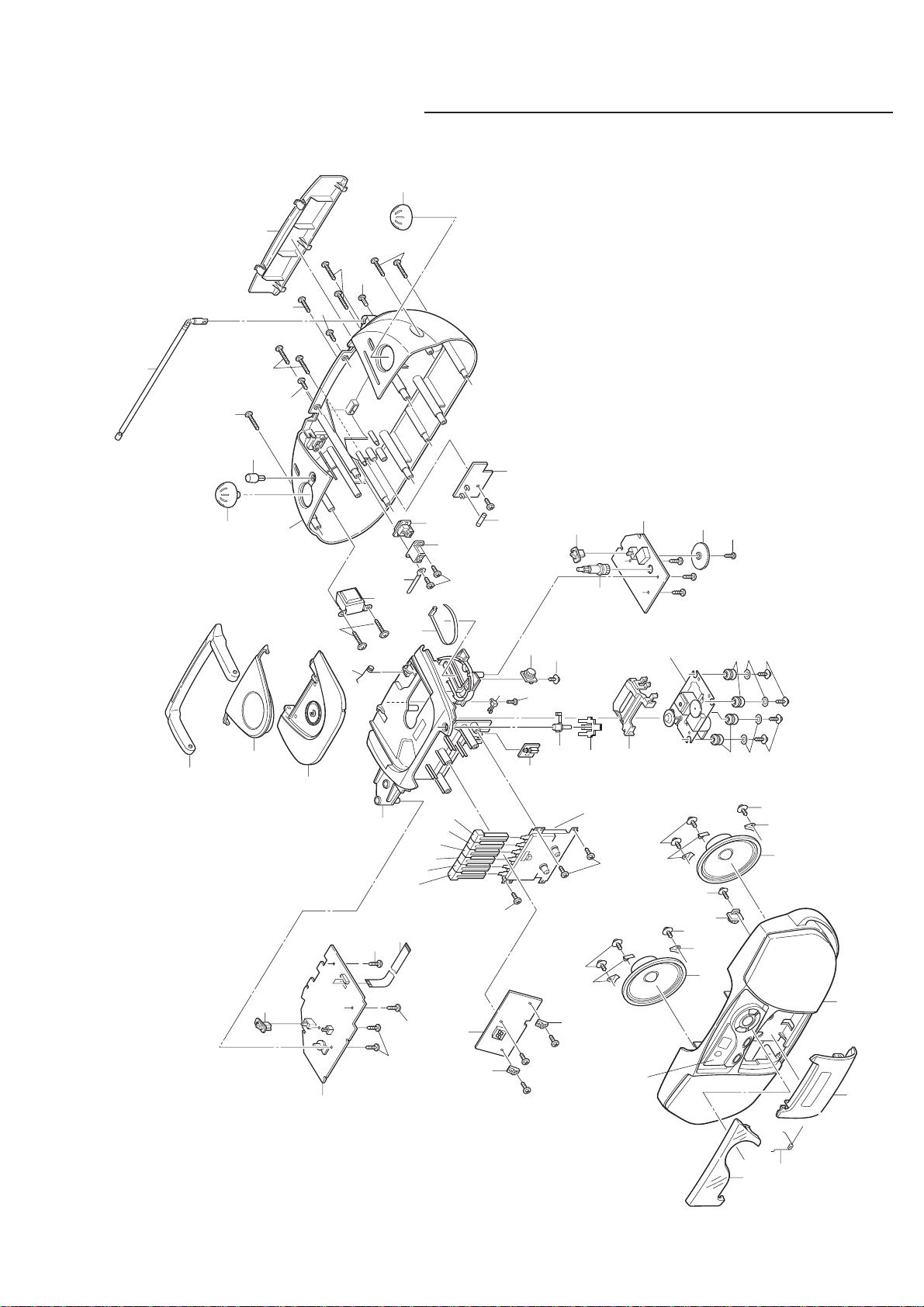
EXPLODED VIEW(CABINET & CHASSIS)
1
4
5
51
9
Y06
Y06
Y06
Y11
Y12
Y12
Y13
Y13
Y14
Y16
Y18
Y17
Y20
Y20
Y20
Y22
Y22
Y23
Y20
Y20
Y01
51
Y02
Y02
7
Y02
Y03
Y03
7
7
Y02
7
6
6
Y01
3
10
11
12
14
15
15
25
16
17
18
21
23
26
27
28
71
72
73
74
29
29
30
32
33
34
35
36
57
40
41
31
24
13
52
54
53
55
56
75
81
43
42
MCD-Z130F/XE.MT
2001 04
- 6 -
Page 8

PARTS LIST
PRODUCT SAFETY NOTICE
EACH PRECAUTION IN THIS MANUAL SHOULD BE FOLLOWED DURING SERVICING. COMPONENTS IDENTIFIED WITH THE
!!
!
IEC SYMBOL
OF SPECIAL SIGNIFICANCE. WHEN REPLACING A COMPONENT IDENTIFIED , USE ONLY THE REPLACEMENT PARTS
DESIGNATED, OR PARTS WITH THE SAME RATINGS OF RESISTANCE, WATTAGE OR VOLTAGE THAT ARE DESIGNATED
IN THE PARTS LIST IN THIS MANUAL. LEAKAGE-CURRENT OR RESISTANCE MEASUREMENTS MUST BE MADE TO
DETERMINE THAT EXPOSED PARTS ARE ACCEPTABLY INSULATED FROM THE SUPPLY CIRCUIT BEFORE RETURNING
THE PRODUCT TO THE CUSTOMER.
CAUTION : Regular type resistors and capacitors are not listed. To know those values, refer to the schematic diagram.
IN THE PARTS LIST AND THE SCHEMATIC DIAGRAM DESIGNATE COMPONENTS IN WHICH SAFETY CAN
Regular type resistors are less than 1/4W carbon type and 0 ohm chip resistors.
Regular type capacitors are less than 50V and less than 1000µF of Ceramic type and Electrolytic type.
PACKING & ACCESSORIES
REF.NO. PART NO. DESCRIPTION
645 027 2073 POLY BAG,PWR CORD
645 035 1334 POLY BAG PE 18 X 24,UNIT
645 044 1943 POLY BAG,I/B
645 051 7136 INSTRUCTION MANUAL(CA)
645 051 7143 INSTRUCTION MANUAL(PA)
645 051 7150 INSTRUCTION MANUAL(XE)
645 051 7167 INSTRUCTION MANUAL(MX)
645 051 7174 INSTRUCTION MANUAL(UK)
645 051 7181 INSTRUCTION MANUAL(AU)
645 051 7198 QUICK GUIDE,GREEK,ARABIA(XE)
645 051 7266 POLY FOAM,2 PCS LEFT&RIGHT
645 051 7358 CARTON CASE(CA)
645 051 7365 CARTON CASE(PA)
645 051 7372 CARTON CASE(130/XE)
645 051 7389 CARTON CASE(MX)
645 051 7396 CARTON CASE(UK)
645 051 7402 CARTON CASE(130/AU)
645 051 7419 CARTON CASE(128/AU)
645 051 7426 CARTON CASE(128/XE)
!!
!
645 023 3463 POWER CORD,VDE APP(XE,PA)
!!
!
645 033 4917 PWR CORD,BSI APP(UK)
!!
!
645 033 7055 PWR CORD,SAA APP(AU)
!!
!
645 041 7160 AC CORD,UL APP(CA,MX)
645 041 9812 REMOTE CTL,RC06-1000A8-010
(All except 128 series)
CABINET & CHASSIS
REF.NO. PART NO. DESCRIPTION
1 645 051 6429 ASSY CASS LID(128 series)
1 645 051 6412 ASSY CASS LID
1 645 051 6436 ASSY CASS LID(PA)
3 645 042 1181 CASS DOOR SPRING
4 645 051 7105 CD DISPLAY LENS
5 645 051 6351 ASSY CABINET
5 645 051 6344 ASSY CABINET
(240/MX)(130/CA)(130/UK)(130/XE)
6 645 033 4252 ASSY,GEAR,S905
7 645 033 0360 SPK CLIP
9 645 051 6863 KNOB CASS PAUSE
10 645 051 6870 KNOB CASS STOP/EJECT
11 645 051 6887 KNOB CASS FFWD
12 645 051 6894 KNOB CASS REWIND
13 645 051 6900 KNOB CASS PLAY
14 645 051 6917 KNOB CASS RECORD
15 645 051 6948 CTL BD HOLDER,FOR DISPLAY
16 645 051 6849 KNOB LEVEL,FUNCTION
17 645 051 6788 HANDLE(Except 128/XE)
17 645 051 6795 HANDLE(128/XE)
18 645 051 6993 CD DOOR
(Except PA, 128 series)
(128/AU)(130/PA)(128/XE)
(130/AU)
REF.NO. PART NO. DESCRIPTION
21 645 051 6405 ASSY CD LID LENS
23 645 051 6986 CD TRAY,TO PANEL
24 645 042 0351 CD DOOR SPRING
25 645 051 6856 DIAL POINTER
26 645 051 7006 CD DOOR KNOB,OPEN
27 645 051 6979 CD DOOR LOCK,FOR TOP PANEL
28 645 042 0375 CD MECHA COVER
29 645 033 3446 RUBBER SILICON
30 645 051 6924 TUNING DRUM
31 645 051 6931 TUNING KNOB GEAR
32 645 051 6832 KNOB LEVEL,BAND
33 645 033 0391 AC SKT COVER
34 645 051 6368 ASSY CABINET REAR
(128/AU)(130/PA)(130/AU)(130/XE)
34 645 051 6375 ASSY CABINET REAR(240/MX)(130/CA)
34 645 051 6382 ASSY CABINET REAR(130/UK)(128/XE)
35 645 051 6825 KNOB ROTARY,VOL
36 645 051 6818 KNOB PUSH,BASSXPANDER
40 645 051 6801 KNOB ROTARY,TUNING
41 645 051 6771 BATTERY LID
42 645 051 7112 CD DISPLAY,IR(All except 128 series)
42 645 051 7129 CD DISPLAY(128 series)
43 645 042 0313 CD DECK MECHANISM,13930400
FIXING PARTS
REF.NO. PART NO. DESCRIPTION
Y01 645 027 1168 SCR 3X8,GEAR
Y02 645 027 1168 SCR 3X8,SPK
Y03 645 023 6617 SCREW ST 3X10,CASS DECK
Y06 645 023 6594 SCREW ST 3X8,CD BD
Y11 645 033 4276 SCR 2X6,CD LEAF SW
Y12 645 027 1373 WASHER METAL,MAIN
Y13 645 033 0247 SCR 2.6X8,CD DECK
Y14 645 033 1527 SCR 2.6X6,TUNING DRUM
Y16 645 027 1182 SCR 3X20,PWR TRANS
Y17 645 027 1328 SOLDERING SLUG,FCCX3
Y18 645 027 1144 SCR 2.8X12,AC SOCKET
Y20 645 027 3841 SCR 3X2.5,F CAB TO B CAB
Y22 645 027 1199 SCR 3X30,F CAB TO B CAB,B CAB TO
Y23 645 027 1236 SCR 3X8,ROD ANT
ELECTRICAL-PARTS
REF.NO. PART NO. DESCRIPTION
51 645 042 3307 SPK 4, SPK
52 645 042 0207 FFC CABLE 15PINS,
53 645 043 9780 LEAF SW,CD LID SW
!!
54
54
54
54
55
55
!
645 041 9881 PWR TRANS,V3023FS(UK,XE)
!!
!
645 041 9898 PWR TRANS,V3024FS(AU)
!!
!
645 042 9439 PWR TRANS,D1110(CA,MX)
!!
!
645 046 1576 PWR TRANS,V3011FS(PA)
!!
!
645 032 9760 AC SOCKET S-1-1225,VDE
!!
!
645 041 9935 AC SOCKET HJC-022A(CA,MX)
CD CN901 TO CD DECK
(All except CA,MX)
- 7 -
Page 9

PARTS LIST
REF.NO. PART NO. DESCRIPTION REF.NO. PART NO. DESCRIPTION
!!
56
56
57 645 041 9928 ROD ANTENNA,2 SECTION
!
645 035 0092 GLASS TUBE FUSE 2 A,FS1101
(All except MX,CA)
!!
!
645 051 6504 FUSE GLASS TUBE,FS1101(MX,CA)
!!
!
645 023 6358 SW SLIDE SS12J01M65(PA)
645 051 6696 PVC PLATE,FOR VOLTAGE HOLE
(Except PA)
!!
!
645 027 0352 CHOKE COIL 100UH,MOTOR
645 033 3606 FERRITE BEAD,
CABLE ACROSS CD PCB(128 series)
645 042 0191 HSG 4PINS,
CN1102 TO RECTIFIER CN11
(128 series)
645 042 0221 SHIELD W TRIPPLE COR,
CASS DECK TO MAIN
645 042 9569 HSG 6P,TO CD DECK
645 042 9590 HSG 2P,TO CTL CN705
645 044 9284 FERRITE BEAD,FORMER PRIMARY
WIRE(All except 128 sereis)
645 051 6474 FERRITE BEAD,FORMER PRIMARY
WIRE(128 sereis)
645 044 9284 FERRITE BEAD,FORMER
SECONDARY WIRE(Except 128 sereis)
645 051 6474 FERRITE BEAD,FORMER
SECONDARY WIRE(128 sereis)
645 051 6566 3P HSG,TO CTL CN702
(All except 128 sereis)
645 051 6573 4P HSG,CN1102 TO RECTIFIER CN11
(All except 128 sereis)
645 051 6580 4P HSG,SPK TO MAIN CN301
645 051 6597 5P HSG,TO TUN CN101
645 051 6603 6P HSG,TO CTL CN701
645 051 6610 8P HSG,CD CN907/CN908 TO CTL CN
645 051 6627 3P HSG,MOTOR TO MAIN CN302
645 051 6634 2P HSG,
CD DOOR SW TO MAIN CN904
645 051 6665 BUFFER,EMC X 8
C0908 403 060 8908 POLYESTER 0.033U M 50V
C0909 403 057 3800 POLYESTER 0.1U M 50V
C0911 403 062 1105 POLYESTER 0.047U M 50V
C0912 403 063 0800 POLYESTER 6800P M 50V
C0928 403 060 8908 POLYESTER 0.033U M 50V
C0930 403 057 1202 POLYESTER 0.01U M 50V
C0932 403 060 8908 POLYESTER 0.033U M 50V
C0933 403 059 0708 POLYESTER 0.018U M 50V
C0934 403 060 6904 POLYESTER 3300P M 50V
C0939 403 060 6904 POLYESTER 3300P M 50V
C0940 403 057 3800 POLYESTER 0.1U M 50V
C0951 403 062 5905 POLYESTER 5600P M 50V
C0952 403 062 5905 POLYESTER 5600P M 50V
C0963 403 057 3800 POLYESTER 0.1U M 50V
CF901 645 042 0115 RESONATOR 16.934MHZ
CN301 645 027 0611 WAFER 4P
CN302 645 032 9982 HEADER 3PINS
CN901 645 042 0177 FFC HEADER 15PINS,
TO PICK UP ASSY
CN904 645 042 9538 HEADER 2PINS,CD LEAF SW
D0301 645 023 6112 RECTIFIER 1N-4001
D0305 645 023 6099 DIODE 1N-4148
D0306 645 023 6099 DIODE 1N-4148
D0901 645 023 6099 DIODE 1N-4148
D0903 645 023 6099 DIODE 1N-4148
D0904 645 023 6099 DIODE 1N-4148
D0905 645 023 6099 DIODE 1N-4148
D0906 645 023 6099 DIODE 1N-4148
D0907 645 023 6099 DIODE 1N-4148
IC201 645 033 4696 IC TA2068N
IC301 645 049 9890 IC LA4627
IC901 645 041 9980 IC LA9250M
IC902 645 041 9997 IC LC78602YE
IC903 645 044 3022 IC MM1469XH
IP901 645 033 4672 IC PROTECTOR N15,ICP901
JK301 645 033 3743 EARPHONE JACK
L0301 645 044 1721 FERRITE BEAD
L0302 645 044 1721 FERRITE BEAD
CD MAIN/AMP P.W.BOARD ASSY
REF.NO. PART NO. DESCRIPTION
71 614 320 1731 ASSY,PWB,CD MAIN/AMP(Only initial)
(130/PA)(130/UK)(130/AU)(130/XE)
71 614 321 0818 ASSY,PWB,CD MAIN/AMP(Only initial)
(MX, CA)
71 614 321 0832 ASSY,PWB,CD MAIN/AMP(Only initial)
(128 series)
C0201 403 060 6904 POLYESTER 3300P M 50V
C0202 403 060 6904 POLYESTER 3300P M 50V
C0207 403 059 6908 POLYESTER 0.022U M 50V
C0208 403 059 6908 POLYESTER 0.022U M 50V
C0209 403 059 4409 POLYESTER 2200P M 50V
C0210 403 059 4409 POLYESTER 2200P M 50V
C0223 403 059 4409 POLYESTER 2200P M 50V
C0224 403 059 6908 POLYESTER 0.022U M 50V
C0225 403 057 1202 POLYESTER 0.01U M 50V
C0310 403 058 6008 POLYESTER 0.15U M 50V
C0311 403 058 6008 POLYESTER 0.15U M 50V
C0315 403 045 1801 ELECT 1000U M 25V
C0501 403 060 6904 POLYESTER 3300P M 50V
C0502 403 060 6904 POLYESTER 3300P M 50V
C0505 403 058 6008 POLYESTER 0.15U M 50V
C0506 403 058 6008 POLYESTER 0.15U M 50V
C0901 403 059 4409 POLYESTER 2200P M 50V
C0902 403 057 3800 POLYESTER 0.1U M 50V
C0903 403 057 3800 POLYESTER 0.1U M 50V
C0904 403 062 1105 POLYESTER 0.047U M 50V
C0905 403 060 6904 POLYESTER 3300P M 50V
L0303 645 044 1721 FERRITE BEAD
L0901 645 042 0108 CHOKE COIL 26UH
Q0201 645 033 3491 TR 2SC945P
Q0202 645 023 6129 TR 9014C
Q0301 645 023 6129 TR 9014C
Q0302 645 023 6129 TR 9014C
Q0901 645 033 3521 TR 2SA1317S AC
Q0902 645 041 9959 TR 2SA1346AC
Q0903 645 033 3514 TR 2SB764D
Q0904 645 041 9959 TR 2SA1346AC
Q0905 645 033 3538 TR 2SD1936S AC
Q0906 645 033 3538 TR 2SD1936S AC
Q0907 645 023 6129 TR 9014C
R0303 402 071 1304 FUSIBLE RES 2.2 JA 1/4W
R0304 402 071 1304 FUSIBLE RES 2.2 JA 1/4W
SW301 645 042 0054 SW SLIDE,SS23E01G6
SW501 645 042 0030 SW PUSH,ON-OFF
T0201 645 027 0307 BIAS COIL,IFT 3630
VR301 645 042 0085 ROTARY VR,SHAFT VOL
645 027 1267 COPPER WIRE
645 027 1267 COPPER WIRE
645 027 1281 COPPER WIRE
645 027 1298 EYELET
645 027 1397 NUT
645 033 0285 COPPER WIRE
645 033 0285 COPPER WIRE
645 033 0322 TUBE COTTON SLEEVE
645 042 0337 HEAT SINK
645 043 9803 HEAT SINK
- 8 -
Page 10

PARTS LIST
DISPLAY P.W.BOARD ASSY
REF.NO. PART NO. DESCRIPTION
72 614 320 1755 ASSY,PWB,DISPLAY(Only initial)
(240,130 series)
72 614 321 0795 ASSY,PWB,DISPLAY(Only initial)
(128 series)
CN701 645 051 6542 6P HEADER
CN702 645 051 6528 3P HEADER(240,130 series)
CN703 645 051 6559 8P HEADER
CN705 645 051 6511 2P HEADER
D0701 645 023 6099 DIODE 1N-4148
D0703 645 023 6099 DIODE 1N-4148
D0704 645 023 6099 DIODE 1N-4148
D0705 645 023 6099 DIODE 1N-4148
D0706 645 023 6099 DIODE 1N-4148
D0707 645 023 6099 DIODE 1N-4148
D0708 645 023 6099 DIODE 1N-4148
D0709 645 023 6099 DIODE 1N-4148
D0710 645 023 6099 DIODE 1N-4148
D0711 645 023 6099 DIODE 1N-4148
D1201 645 033 3477 DIODE RPM-6938-V4(240,130 series)
Q0701 645 033 3521 TR 2SA1317S AC
Q0702 645 033 3521 TR 2SA1317S AC
Q0703 645 023 6129 TR 9014C
Q0704 645 023 6129 TR 9014C
SW701 645 042 0023 SW TACT,MEMORY
SW702 645 042 0023 SW TACT,REPEAT
SW703 645 042 0023 SW TACT,FB-B-SCAN
SW704 645 042 0023 SW TACT,FF-F-SCAN
SW705 645 042 0023 SW TACT,STOP/CLEAR
SW706 645 042 0023 SW TACT,PLAY/PAUSE
645 042 0078 LED DISPLAY
645 042 0795 LED BRACKET
645 051 6481 LED ROUND TYPE,REPEAT
645 051 6481 LED ROUND TYPE,MEMORY
645 051 6481 LED ROUND TYPE,PLAY/PAUSE
645 023 6594 SCREW ST 3X8
645 023 6617 SCREW ST 3X10
645 033 0285 COPPER WIRE,JW701,702
645 027 1267 COPPER WIRE,JW703
REC SW P.W.BOARD ASSY
REF.NO. PART NO. DESCRIPTION
73 614 320 1779 ASSY,PWB,REC SW(Only initial)
645 051 6498 5P CONNECTOR,TO MAIN CN204
SW801 645 033 3569 PUSH SW,PS-22F03
TUNER P.W.BOARD ASSY
REF.NO. PART NO. DESCRIPTION
74 614 320 1748 ASSY,PWB,TUNER(Only initial)(XE)
74 614 321 0788 ASSY,PWB,TUNER(Only initial)(UK)
74 614 321 0825 ASSY,PWB,TUNER(Only initial)
(MX)(CA)
74 614 321 0849 ASSY,PWB,TUNER(Only initial)
(AU)(PA)
C0114 403 056 8905 POLYESTER 1000P M 50V
C0120 645 051 6443 POLYESTER 140PF
C0129 403 059 0708 POLYESTER 0.018U M 50V
C0130 403 059 0708 POLYESTER 0.018U M 50V
CF102 645 051 6450 CERAMIC FILTER
CF103 645 027 0291 CERAMIC FILTER(Except UK,XE)
CF103 645 041 9966 CERAMIC FILTER(UK,XE)
CF104 645 051 6467 BAND PASS FILTER
CN101 645 051 6535 5P HEADER,V- TYPE
CT105 645 033 4771 TRIMMER 20PF(UK)
CT106 645 033 4771 TRIMMER 20PF(UK)
D0101 645 023 6099 DIODE 1N-4148
D0102 645 023 6099 DIODE 1N-4148
D0103 645 023 6082 DIODE 1S-2638,AFC
REF.NO. PART NO. DESCRIPTION
D0104 645 023 6105 ZENER DIODE
D0105 645 023 6099 DIODE 1N-4148
IC101 645 041 9973 IC LA1824
L0104 645 023 6297 VHF COIL
L0105 645 032 9944 FTZ COIL,BH-816557
L0106 645 024 1024 AM COIL
L0107 645 042 0016 LW COIL(UK)
PVC01 645 026 6676 PVC,AM/FM
SW101 645 042 0047 SW SLIDE SS22E01G6,2 BAND SW
(Except UK)
SW101 645 042 0061 SW SLIDE SS63D01GT6,3 BAND SW
(UK)
SW102 645 024 1048 SW SLIDE SK22F03G6,
MONO & BEAT CUT SW
T0101 645 026 6669 AM OSC,OSC 1010
T0102 645 026 6669 AM OSC,OSC 1010(UK)
T0103 645 027 0437 FM IFT,IF 0070
T0104 645 033 3866 AM COIL,IF 2070
T0105 645 027 0444 FM IFT,IF 0380
645 042 0184 HSG 1PIN,FM ANT
645 042 0344 CONTACT PIN,FM ANT
645 033 0285 COPPER WIRE
645 027 1267 COPPER WIRE,
645 014 4646 COPPER WIRE
645 027 1274 COPPER WIRE,
645 023 6594 SCREW ST 3X8
645 051 6320 ASSY BAR ANT(Except UK)
645 051 6337 ASSY BAR ANT(UK)
645 024 1055 FERRITE BAR(Except UK)
645 025 4338 FERRITE BAR( UK)
645 051 6658 BAR ANT HOLDER
RECTIFIER P.W.BOARD ASSY
REF.NO. PART NO. DESCRIPTION
75 614 320 1762 ASSY,PWB,RECTIFIER(Only initial)
(All except MX,CA)
75 614 321 0801 ASSY,PWB,RECTIFIER(Only initial)
(MX,CA)
C1105 403 135 0400 ELECT 3300U M 25V
D0401 645 033 3859 ZENER 8.2V
D1101 645 023 6112 RECTIFIER 1N-4001(240/MX)(130/CA)
D1102 645 023 6112 RECTIFIER 1N-4001
D1103 645 023 6112 RECTIFIER 1N-4001
D1104 645 023 6112 RECTIFIER 1N-4001
F1101 645 035 0092 GLASS TUBE FUSE 2 A,FS1101
(All except MX,CA)
F1101 645 051 6504 FUSE GLASS TUBE,FS1101(MX,CA)
N1101 645 027 0611 WAFER 4P,CN1101
Q0401 645 033 3507 TR 2SD2061E
645 035 0511 FUSE HOLDER MW1010K
645 042 0320 HEAT SINK
645 023 6594 SCREW ST 3X8
645 023 6686 SCREW M3X8,FOR IC
645 033 0285 COPPER WIRE,JW1101,1102
645 027 1298 EYELET
645 027 1397 NUT
- 9 -
Page 11

EXPLODED VIEW & PARTS LIST (TAPE DECK MECHANISM)
TAPE DECK MECHANISM CHASSIS
REF.NO. PART NO. DESCRIPTION
81 645 050 1814 CASS DECK MECHANISM
TM01 645 018 0637 R/P HEAD
TM02 645 050 0985 PINCH ROLLER ARM
TM03 645 030 6839 E HEAD
TM04 645 050 1395 RF BELT
TM05 645 050 1784 MAIN BELT
TM06 645 050 2101 ASSY,MOTOR
TM03
TM01
TM02
TM04
TM05
TM06
IC BLOCK DIAGRAM & DESCRIPTION
IC101 LA1824 (Tuner)
IC903 MM1569XH (CD Driver)
24
23 22 21
FM
RF
AM
RF
1
234
FM
MIX
AM
MIX
AM
OSCREG Vcc1
20
19 18 17
FM
Vcc2GND2
OSC
TRIG ST-SW VCO
GND1
5
678
IC201 TA2068 (Cassette Priamp.)
DECODER
TUN
LED
16
15 14 13
PHASE
COMP
FF FF FF
S-METER
ST
FM-IF
LED
9
10 11 12
PILOT
DET
DET
AM-IF
DET
AGC
28 27 26 25 24 23 22 21 20 19 18 17 16 15
Vcc
Level shift
T.S .D
Level shift
1234567 891011121314
Vcc
D.BUFD.BUFD.BUFD.BUF
Level shift
DRIVER MUTE
Level shift
D.BUFD.BUFD.BUFD.BUF
- 10 -
Page 12

IC BLOCK DIAGRAM & DESCRIPTION
IC901 LA9250M (Analog Signal Processor)
No. Pin Name
1 FTN2
2 FTN1
3E
4F
5TB
6 TE7TE
8 TSEI
9 SCI
10 TH
11 TA
12 TD13 TD
14 JP
15 TO
16 N C
17 FD
18 FD-
19 FA
20 FA21 FE
22 FE23 SP
24 SPG
25 SP26 SPD
27 SLEQ
28 SLD
29 SL30 SL+
31 OSC
32 N C
Function
Pick-up photo-diode connection pin. Added to FTN! Pin to generate the
RF signal, subtracted from FTN1 pin to generate the FE signal.
Pick-up photo-diode connection pin.
Pick-up photo-diode connection pin. Subtracted from F pin to generate
the TE signal.
Pick-up photo-diode connection pin.
TE signal DC component input pin.
PIN which connect the TE signal gain setting resistor between this pin
and TE pin.
TE signal output pin.
TES(Track Error Sense)comparator input pin. The TE signal is input
thorough a band-pass filter.
Shock detection input pin.
Tracking gain time constant setting pin.
TA amplifier output pin.
Pin for configuring the tracking phase compensation constant between
the TD and VR pin.
Tracking phase compensation setting pin.
Tracking jump signal(kick pulse)amplitude setting pin.
Tracking control signal output pin.
No connection
Focusing control signal output pin.
Pin for configuring the focusing phase between the FD and FA pins.
Pin for configuring the focusing phase compensation constant the FDand FA- pins.
Pin for configuring the focusing phase compensation constant between
the FAS and FE pins.
FE signal output pin.
Pin which connects the FE signal setting resistor between this pin and
FE pin.
Inverted output of CLV pin signal.
12-cm spindle mode gain setting resistor connection pin.
Spindle phase compensation constant pin, along with SPD pin.
Spindle control signal output pin.
Sled phase compensation constant connection pin.
Sled control signal output pin.
Input pin for sled movement signal from microprocessor.
Input pin for sled movement signal from microprocessor.
Pin for setting oscillating frequency.
No connection.
No. PIN NAME Function
33 SLOF Sled servo off control input pin.
34 TGRF
35 SP8 Switch control pin for spindle 8cm/12cm mode.
36 EFBAL E/F balance control signal input.
37 FSTA Focus search control signal input.
38 LASER Laser on/off control input.
39 NC No connection.
40 TJP Input pin for tracking jump signal from DSP.
41 TGL
42 TOFF
43 TES Output pin for TES signal to DSP.
4 4 HFL
45 CLV Input pin for CLV error signal from DSP.
46 GND GND
47 RF RF output pin.
48 RF-
49 SLC
50 SLI Input pin used by DSP for controlling the date slice level.
51 DEF Disc defect detection output pin.
52 DRF RF level detection output(Detect RF)
53 FSC Focus search smoothing capacitor output pin.
54 TBC
55 FSS
56 VCC VCC
5 7 REFI By-pass capacitor connection pin for reference voltage.
58 VR Reference voltage output pin.
59 LF2 Disc defect detection time constant setting pin.
60 PH1 RF signal peak hold capacitor connection pin.
61 BH1 RF signal bottom hold capacitor connection pin.
62 LDD APC circuit output pin.
63 LDS APC circuit input pin.
64 NC No connection.
Pin for setting the function on/off, which function is tracking gain
following to RF level.
Input pin for tracking gain control signal from DSP. Gain is low when
TGL is high.
Input pin for tracking off control signal from DSP. Tracking servo is off
when TOFF is high.
The High Frequency Level is used to determine whether the main beam
is positioned over a pit or over the mirrored surface.
RF gain setting and EFM signal 3T compensation constant setting pin,
along with the RF pin.
Slice Level Control is an output pin that control the date slice level used
by the DSP for the RF wave-form.
Tracking Balance Control; E/F balance adjustment variable range
setting pin.
Focus Search Select; focus search mode(+-search / + search vs. the
reference voltage) switching pin.
- 11 -
Page 13

IC BLOCK DIAGRAM & DESCRIPTION
IC902 LC78602YE (Analog Signal Processor)
No. Pin Name
1 DEF1
2 3V / *5V
3 PDO
4 VVss
5 ISET
6 VVdd
7FR
8 Vss
9 EFMO
10 EFMIN
11 TMOD
12 CLV
1 3 HFL
14 TES
15 TOFF
16 TGL
17 JP
18 LASER
19 FSTA
20 EFBAL
21 SP8
22 Vdd
23 FSEQ
24 PCK
25 SLOF
26 SLED+
27 SLED28 PUIN
29 DOUT
30 NC
31 *SEG8
32 *SEG7
Function
It is junction in unused time, 0 V defect detecting signal (DEF) input
terminal
It is 5 V use 3 V use, L H power supply voltage selection input terminal.
The phase comparison output terminal for outside VCO control(PLL
control)
Earth terminal for internal organs VCO control , connecting it to 0 V by
all means
Resistance connection terminal for electric current adjustment of PDO
output
Power supply terminal for internal VCO control
VCO frequency range adjustment control
Digital series earth terminal. Being connected to 0 V by all means.
EFM signal output terminal.(Slice level control )
EFM signal input terminal.(Slice level control )
Input terminal for a test. (Being connected to 0 V by all means)
The output terminal for disk motor control. 3 value output
Truck detecting signal input terminal.
Tracking error signal input terminal.
Tracking OFF output terminal
The output terminal for tracking gain change. (Go up gain with L)
The output terminal for tracking jump control. (3 value output)
Laser control terminal. (The pull-down resistor internal )
The FS TA control terminal. (The pull-down resistor internal )
EFBAL control terminal. (The pull-down resistor internal )
SP 8 control terminal. (The pull-down resistor internal )
Digital series power supply terminal
The synchronising signal search output terminal. When synchronising
signal of inside creation agreed with the synchronising signal which
detected it from EFM signal, it become "H"
Clock monitor terminal for EFM data reproduction. ( Limited at the time
of test mode but)
Thread OFF control output terminal
The thread field output terminal
The thread field output terminal
Limit switch sensing input terminal. (The pull-up resister internal )
Digital OUT output terminal. (EIAJ format)
NC (Being open)
The segment output (8) terminal. (The pull-up resister internal )
The segment output (7) terminal. (The pull-up resister internal )
- 12 -
No. PIN NAME Function
33 *SEG6 The segment output (6) terminal. (The pull-up resister internal )
34 *SEG5 The segment output (5) terminal. (The pull-up resister internal )
35 *SEG4 The segment output (4) terminal. (The pull-up resister internal )
36 *SEG3 The segment output (3) terminal. (The pull-up resister internal )
37 *SEG2 The segment output (2) terminal. (The pull-up resister internal )
38 *SEG1 The segment output (1) terminal. (The pull-up resister internal )
3 9 Vcc Digital series earth terminal. (It is connection in 0 V by all means)
40 NC NC
4 1 *DIG2 The common drive output (2) terminal.The pull-up resister internal
4 2 *DIG1 The common drive output (1) terminal.The pull-up resister internal
4 3 *PROG
Program movement monitor output terminal. (The pull-up resister
internal )
44 *KEYIN Key matrix input terminal. (The pull-up resister internal )
45 NC NC (Being open)
46 NC NC (Being open)
47 *RANDOM Random mode display output terminal
4 8 RMTSL3 The wireless remote controller identification input (3) terminal
49 EFLG C1 , C2 , 1 fold , 2fold Correction monitor
50 FSX
7.35KHz synchronizing signal output terminal which did dividing from
OSC. As a condition, Limited at the time of test mode
51 *AMUTE audio , Mute output signal
5 2 REMOTE Wireless remote controller signal input terminal
5 3 RMTSL2 Wireless remote controller identification input(2) terminal
54 LCHO D/A , L channel output terminal
5 5 L/R Vdd D/A control power source terminal
5 6 L/RVss D/A control earth terminal. (It is connection in 0 V by all means)
57 RCHO D/ A , R channel output terminal
58 CLOSE Closing switch sensing input terminal. The pull-up resister internal
5 9 RMTSL1
Wireless remote controller identification input(1) terminal. (The pull-up
resister internal )
60 Xout Connection terminal of 16.9344 MHz crystal OSC
6 1 Xin Connection terminal of 16.9344 MHz crystal OSC
62 XVdd Power supply terminal for crystal OSC
6 3 *RES Reset input terminal
6 4 DRF DRF input terminal
Page 14

)
)
)
)
)
)
IC & TRANSISTOR VOLTAGES
IC901 LA9250M (CD PLAY MODE
Pin No. 12345678910111213141516
Voltage 2.5 2.5 2.5 2.5 2.5 2.5 2.5 2.57 2.57 2.5 2.55 2.57 2.57 2.57 2.55 0
Pin No. 17 18 19 20 21 22 2 3 24 25 26 27 28 29 3 0 31 32
Voltage 2.77 2.57 2.4 2.57 2.5 2.5 2.47 2.47 2.5 3.0 2.56 0.2 2.2 2.37 1.5 0
Pin No. 33 34 35 36 37 38 39 40 4 1 42 43 44 45 46 47 48
Voltage 0 0.1 0 0.45 0.45 5.15 0 2.56 5.1 0 1.5 0 2.8 0 2.41 2.57
Pin No. 49 50 51 52 53 54 55 56 5 7 58 59 60 61 62 63 64
Voltage 2.5 2.01 0 5.0 2.5 2.5 0 5.1 2.5 2.5 2.57 2.54 2.2 3.9 0.1 0
IC902 LC78602E (CD PLAY MODE
Pin No. 12345678910111213141516
Voltage 0 0 1.61 0 1.5 5.15 0.36 0 2.5 2.4 0 2.91 0 1.6 0 5.15
Pin No. 17 18 19 20 21 22 23 24 2 5 26 27 28 29 30 31 32
Voltage 2.55 5.15 0.44 0.45 0 5.1 5.1 000002.603.02 3.04
Pin No. 33 34 35 36 37 38 39 40 4 1 42 43 44 45 46 47 48
Voltage 3.04 2.96 3.02 3.03 5.12 2.71 2.72 0 2.9 2.8 5.14 5.14 0000
Pin No. 49 50 51 52 53 54 55 56 5 7 58 59 60 61 62 63 64
Voltage 0 0 5.1 5.07 0 1.84 4.4 0 1.8 0 0 2.1 2.1 5.1 5.12 5.0
IC903 MM1469 (CD PLAY MODE
Pin No. 12345678910111213141516
Voltage 3.6 3.7 2.5 2.5 7.05 5.1 5.1 0 2.5 2.55 3.61 3.55 0 7.3 0.55 0.71
Pin No. 17 18 19 20 21 22 23 24 2 5 26 27 28
Voltage 3.3 3.95 3.91 2.8 2.5 7.82 7.81 2.5 2.6 3.75 3.75 0
(V)
(V)
(V)
IC101 LA1824 (RADIO MODE
Pin No. 12345678910111213141516
AM Voltage 1.27 1.27 4.96 4.9 4.9 0 4.9 0 0 1.27 1.26 0.6 4.9 0 0 1.3
FM Voltage 1.2 1.2 4.91 4.91 4.91 0 4.9 0 0 1.2 1.2 0 4.9 4.1 4.1 1.3
Pin No. 17 18 19 20 21 22 23 24
AM Voltage 1. 3 1.2 0.41 4.97 4.97 4.97 0 0
FM Voltage 1.3 1.2 1.27 4.87 4.87 4.86 0 0.31
IC201 TA2068 (RADIO/TAPE/CD MODE
Pin No. 12345678910111213141516
RADIO Voltage 0 2. 0 2.0 2.0 2.0 2.0 0 2. 0 2.0 2.0 2.0 2.0 2.0 2 . 0 0 2 . 0
TAPE Voltage 0 2. 0 2.0 2. 0 2.0 2.0 0 2.0 2. 0 2.0 2. 0 2.0 2.0 2. 0 6.2 2. 0
CD Voltage 0 2.0 2. 0 2.0 2.0 2.0 0 2. 0 2.0 2.0 2.0 2.0 2.07 2.07 0 2.0
Pin No. 17 18 19 20 21 22 23 24
RADIO Voltage 0 2.1 7.6 2.1 0 2.0 0.7 2.0
TAPE Voltage 0 2.0 7.4 2.0 0 2.0 0.7 2.0
CD Voltage 5.9 2.0 7.12 2.0 0 2.07 0.7 2.07
IC301 LA6527 (RADIO/TAPE/CD MODE
Pin No. 123456789101112
RADIO Voltage 1.3 6.02 0 0 0 1.41 1.41 0.27 9.19 0 5.92 12.6
TAPE Voltage 1.3 5.8 0 0 0 1.42 1.42 1.42 9.07 0 5.75 12.64
CD Voltage 1.27 5.12 0 0 0 1.3 1.3 5.5 8.4 0 5.0 11.0
(V)
(V)
(V)
- 13 -
Page 15

SCHEMATIC DIAGRAM (AUDIO for Z130 series)
PRODUCT SAFETY NOTICE
Each precaution in this manual should be followed during servicing. Components identified with the IEC symbol
components in which safety can be of special significance. When replacing a component identified by
same ratings of resistance, wattage or voltage that are designated in the parts list in this manual. Leakage-current or resistance measurements must be made to
determine that exposed parts are acceptably insulated from the supply circuit before returning the product to the customer.
!!
!
in the parts list and the schematic diagram designated
!!
!
, use only the replacement parts designated, or parts with the
- 14 -
Page 16

SCHEMATIC DIAGRAM (AUDIO for Z128 series)
PRODUCT SAFETY NOTICE
Each precaution in this manual should be followed during servicing. Components identified with the IEC symbol
components in which safety can be of special significance. When replacing a component identified by
same ratings of resistance, wattage or voltage that are designated in the parts list in this manual. Leakage-current or resistance measurements must be made to
determine that exposed parts are acceptably insulated from the supply circuit before returning the product to the customer.
in the parts list and the schematic diagram designated
!!
!
!!
!
, use only the replacement parts designated, or parts with the
- 15 -
Page 17

SCHEMATIC DIAGRAM (AUDIO for CWM-240)
PRODUCT SAFETY NOTICE
Each precaution in this manual should be followed during servicing. Components identified with the IEC symbol
components in which safety can be of special significance. When replacing a component identified by
same ratings of resistance, wattage or voltage that are designated in the parts list in this manual. Leakage-current or resistance measurements must be made to
determine that exposed parts are acceptably insulated from the supply circuit before returning the product to the customer.
!!
!
in the parts list and the schematic diagram designated
!!
!
, use only the replacement parts designated, or parts with the
- 16 -
Page 18

SCHEMATIC DIAGRAM (CD for Z130 series)
- 17 -
Page 19

SCHEMATIC DIAGRAM (CD for Z128 series)
- 18 -
Page 20

SCHEMATIC DIAGRAM (TUNER for XE, PA)
- 19 -
Page 21

SCHEMATIC DIAGRAM (TUNER for UK)
- 20 -
Page 22

SCHEMATIC DIAGRAM (TUNER for CA, MX)
- 21 -
Page 23

SCHEMATIC DIAGRAM (TUNER for AU)
- 22 -
Page 24

WIRING DIAGRAM (CD MAIN)
- 23 -
Page 25

WIRING DIAGRAM (TUNER for except UK)
- 24 -
Page 26

WIRING DIAGRAM (TUNER FOR UK)
- 25 -
Page 27

WIRING DIAGRAM (DISPLAY)
- 26 -
Page 28

WIRING DIAGRAM (RECTIFIER , REC SW)
RECTIFIER
REC SW
Aug./ '01 / 2850 BB Printed in Japan
SANYO Electric Co., Ltd.
Osaka, Japan
 Loading...