

Page 1
BiCMOS LSI
Ordering number : EN4908A
63095HA (OT)/92194TH No. 4908-1/7
SANYO Electric Co.,Ltd. Semiconductor Bussiness Headquarters
TOKYO OFFICE Tokyo Bldg., 1-10, 1 Chome, Ueno, Taito-ku, TOKYO, 110-8534 JAPAN
Optical Sensor Switch IC
LV9005M
Overview
The LV9005M is an optical sensor switch IC that is
fabricated in a medium breakdown voltage BiCMOS
process. The LV9005M circuit structure includes a highgain optical sensor amplifier, a comparator, an oscillator
circuit, output drivers, LED drivers, and a synchronous
detection and delay circuit. The use of this IC and a
minimal number of external components allows the
implementations of multifunction high-sensitivity
applications that previously would have only been
possible with a custom optical-switch IC.
Applications
• Factory automation (detectors for many types of parts
and products)
• Home security (doorway and window sensors)
• Office automation equipment
Functions and Features
• Can be used with a wide range of supply voltages; from
5 to 30 V.
• Low power
• Outputs can be selected as PNP or NPN circuit types.
• Built-in high-gain amplifier
• Built-in stability and output display functions
• Supports both reflection and through type applications,
and supports both sense on light and sense on dark
applications.
• Built-in OCP and power on reset functions
• Built-in three-level comparator
• Synchronous detection scheme adopted for robust
performance in the presence of ambient and scattered
light.
• External photodiode detection scheme allows the
LV9005M to support a wide range of application areas.
• Miniature flat package supports high density printed
circuit board mounting.
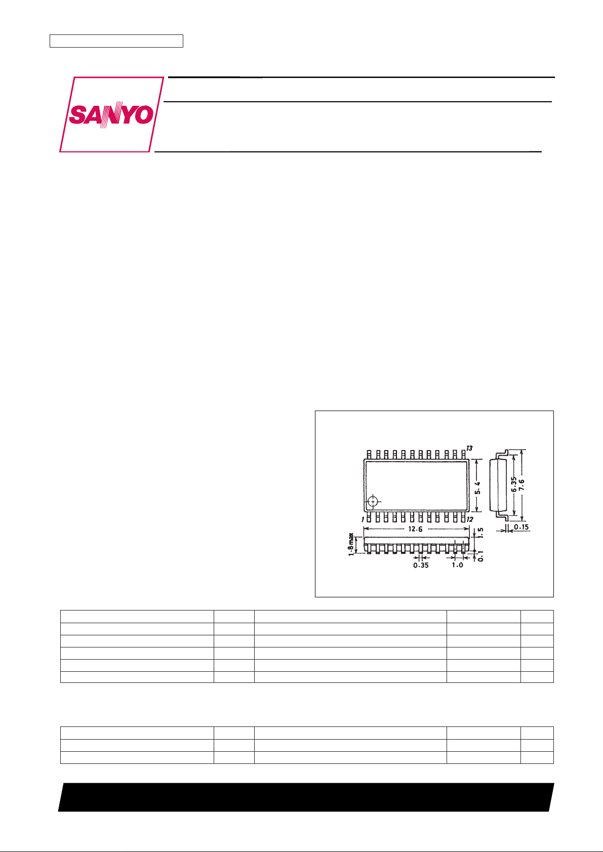
Package Dimensions
unit: mm
3112-MFP24S
SANYO: MFP24S
[LV9005M]
Specifications
Absolute Maximum Ratings at Ta = 25°C
Allowable Operating Ranges at Ta = 25°C
Parameter Symbol Conditions Ratings Unit
Maximum supply voltage V
CC
max 33 V
LD pin voltage V
LD
33 V
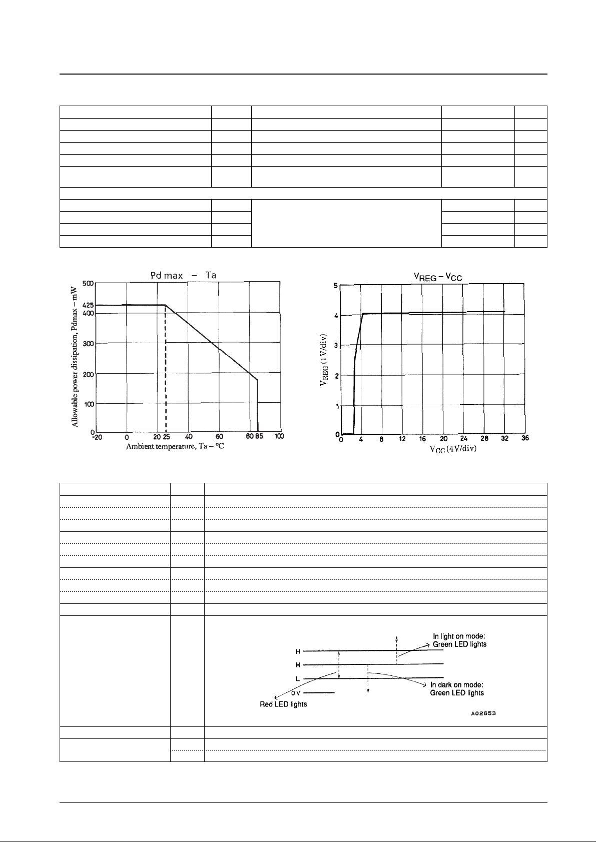
Allowable power dissipation Pd max 425 mW
Operating temperature Topr –20 to +85 °C
Storage temperature Tstg –40 to +125 °C
Parameter Symbol Conditions Ratings Unit
Supply voltage V
CC
4.5 to 30 V
LD pin voltage V
LD
High breakdown voltage input pins VCCto 0 V
Page 2
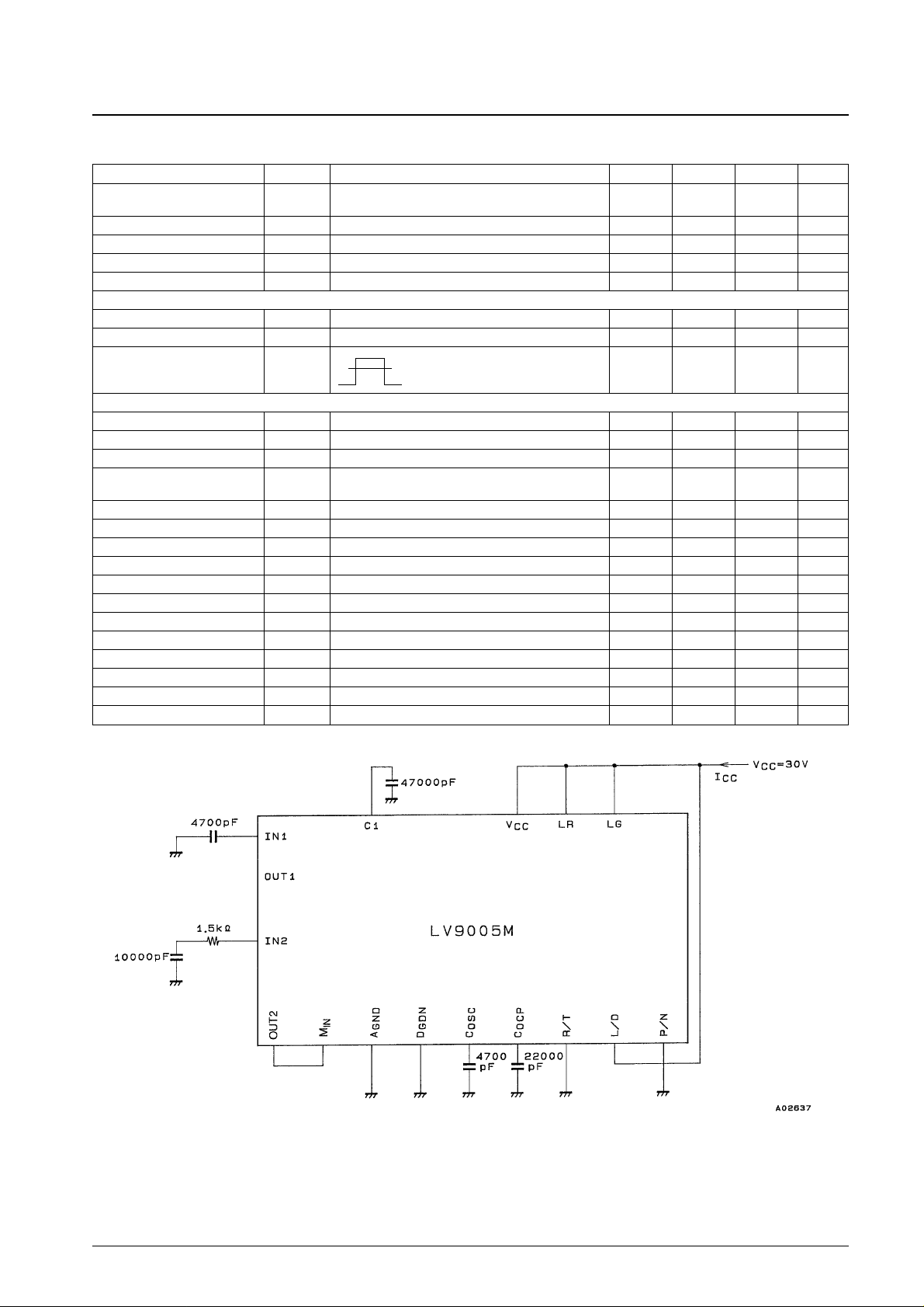
Electrical Characteristics at Ta = 25°C, VCC= 12 V (unless otherwise specified)
Note: * Current drain test circuit
No. 4908-2/7
LV9005M
Parameter Symbol Conditions min typ max Unit
Preamplifier gain V
G1
With a 20 kΩ input series resistance,
15 18 21 dB
f = 200 kHz (sine wave)
Main amplifier gain V
G2
f = 200 kHz (sine wave) 45 48 51 dB
Regulated power supply V
REGVCC
= 5 V, 5 mA DC load 3.72 4.0 4.28 V
Current drain I
CC
Measured in the specified circuit* 3.0 4.5 mA
Input resistance Z
IN
8.5 10 11.5 kΩ
[LED Output Block]
Pulse level V
LEH
With a 1 kΩ external resistor 2.9 3.2 3.6 V
Pulse period T
LE
C
OSC
= 4700 pF 300 380 460 µs
Pulse width T
PW
50% 4.2 5.2 6.2 µs
[Overcurrent Detection Voltage]
PNP output (source) OCP (P) External transistor = PNP V
CC
– 1.1 VCC– 1.35 VCC– 1.6 V
NPN output (sink) OCP (N) External transistor = NPN 1.10 1.35 1.75 V
Comparator detection level (low) COMP
L
0.33 0.44 0.55 V
Comparator detection level
COMP
M
0.60 0.74 0.88 V
(middle)
Comparator detection level (high) COMP
H
1.03 1.16 1.30 V
LG current I
LG
2.05 2.65 3.25 mA
LR current I
LR
1.12 1.72 2.32 mA
PNP drive current (source) I
SRC
1.80 2.85 3.80 mA
NPN drive current (sink) I
SNK
1.90 2.95 3.90 mA
Main amplifier output DC voltage V
OUT2
1.20 1.40 1.56 V
RT input high voltage V
IH
1 4.0 V
RT input low voltage V
IL
1 1.0 V
LD input high voltage V
IH
2 High breakdown voltage input pins 4.0 V
LD input low voltage V
IL
2 High breakdown voltage input pins 1.3 V
P/N input high voltage V
PNH3
4.0 V
P/N input low voltage V
PNL3
1.0 V
Page 3
Design Specifications
Functional Description
No. 4908-3/7
LV9005M
Parameter Symbol Conditions Ratings Unit
Synchronization pull-in range PIR T
EL
= LED pulse period, transmission mode 0.55 TLEto 1.45 T
LE
µs
Power on reset T
POR
13.5 ms
Response time T
D
Oscillator external capacitor C
OCP
= 4700 pF 2 T
LE
µs
Oscillator period T
OSC
Oscillator external capacitor C
OCP
= 4700 pF 380 µs
Hysteresis V
H
0.7 Vp-p
[OCP Pulse]
Pulse period T
OCP (N)
7.0 ms
Pulse width T
OCPW (N)
C
OCP
= 22000 pF
55 µs
Pulse period T
OCP (P)
7.0 ms
Pulse width T
OCPW (P)
55 µs
+0.2
–0.15
Item Symbol Description
R/T SW R/T Reflection/through switching. *: A separate illumination oscillator is used in transmission mode.
Reflect R Input voltage = high (V
REG
) or open
Through T Input voltage = low (GND)
L/D SW L/D Light/dark switching
Light L Input voltage = high (V
CC
) or open
Dark D Input voltage = low (GND)
P/N SW P/N Output PNP/NPN switching
PNP mode PNP Input voltage = high (V
REG
) or open
NPN mode NPN Input voltage = low (GND)
Output protection Built-in overcurrent (load short) protection circuit
Comparator and display ranges
Output type NPN, PNP, two outputs
Mode relationship
Light on mode
→ Light detected: output on, dark detected: output off
Dark on mode → Light detected: output off, dark detected: output on
Page 4

Pin Assignment
Note: The NC pin must not be used.
Pin Functions
No. 4908-4/7
LV9005M
Continued on next page.
Pin No. Symbol I/O circuit type Notes
3
4
5
6
8
9
10
11
IN1
Z
IN
OUT1
IN2
OUT2
M
IN
L/D
Light on mode → V
CC
Dark on mode → 0 V
Reflect mode → 4 V (V
REG
) or open
Through mode → 0 V
R/T
Amplifier first stage input
(Capacitor coupled to the external circuit.)
Photodiode series (load) resistance
(Used when not used with an external resistor.)
Amplifier first stage output
Output amplifier input
Output amplifier output
Comparator middle input (This pin sets the hysteresis. The
hysteresis is maximum when this pin is open, and minimum when
this pin is shorted to pin 8.)
Light/dark mode switching
This pin has a built-in noise filter (delay time: 2T
LE
)
Reflect/through mode switching
Page 5

Continued from preceding page.
No. 4908-5/7
LV9005M
Pin No. Function I/O circuit type Notes
12
14
15
16
18
19
20
21
22
23
P/N
LED OUT
LR
LG
C
OSC
PW
V
REG
C
OCP
NPN
PNP
PNP mode → 4 V (V
REG
) or open
NPN mode → 0 V
V
REG
= VRP(Pin 2)= 4 V
PNP/NPN switching
Light source LED drive output
Red LED (display) connection
Green LED (display) connection
Oscillator capacitor connection
Light source LED pulse width adjustment
(Connect pins 18 and 19 through an external resistor to narrow
the pulse width from the illumination LED.)
Regulator output
OCP pulse oscillator capacitor connection
NPN transistor connection output
PNP transistor connection output
Page 6

Equivalent Circuit Block Diagram
Application Circuit
Note: 1. A
GND
and D
GND
are connected within the IC.
2. The photodiode and LEDs specified here are examples only. The devices actually used should be chosen based on the particular application.
3. The OCP detection level is determined by the voltage across RL plus the Tr2 (or TR1) VBE voltage.
No. 4908-6/7
LV9005M
Page 7

PS No. 4908-7/7
LV9005M
Sample Printed Circuit Board Pattern (copper side)
Sample LV9005M Applications
Through type optoelectronic switch
Reflection type optoelectronic switch
This catalog provides information as of June, 1995. Specifications and information herein are subject to change
without notice.
■ No products described or contained herein are intended for use in surgical implants, life-support systems, aerospace
equipment, nuclear power control systems, vehicles, disaster/crime-prevention equipment and the like, the failure of
which may directly or indirectly cause injury, death or property loss.
■ Anyone purchasing any products described or contained herein for an above-mentioned use shall:
➀ Accept full responsibility and indemnify and defend SANYO ELECTRIC CO., LTD., its affiliates, subsidiaries and
distributors and all their officers and employees, jointly and severally, against any and all claims and litigation and all
damages, cost and expenses associated with such use:
➁ Not impose any responsibility for any fault or negligence which may be cited in any such claim or litigation on
SANYO ELECTRIC CO., LTD., its affiliates, subsidiaries and distributors or any of their officers and employees
jointly or severally.
■ Information (including circuit diagrams and circuit parameters) herein is for example only; it is not guaranteed for
volume production. SANYO believes information herein is accurate and reliable, but no guarantees are made or implied
regarding its use or any infringements of intellectual property rights or other rights of third parties.
 Loading...