

SANYO LV3400M Datasheet
Overview
The LV3400M is a filter IC designed for FM multiplex
broadcast reception and is used in combination with the
Sanyo LC72700 demodulation/error correction IC. The
adoption of switched capacitor (SCF) technology means
that frequency adjustment is not required and that the
LV3400M provides stable operation.
Functions
• 76 kHz band-pass filter (Gaussian filter)
• 54 kHz high-pass filter
• 125 kHz low-pass filter
• Anti-aliasing filter
• Limiter circuit
Features
• Adjustment-free, due to the use of SCF technology.
• Few external components are required.
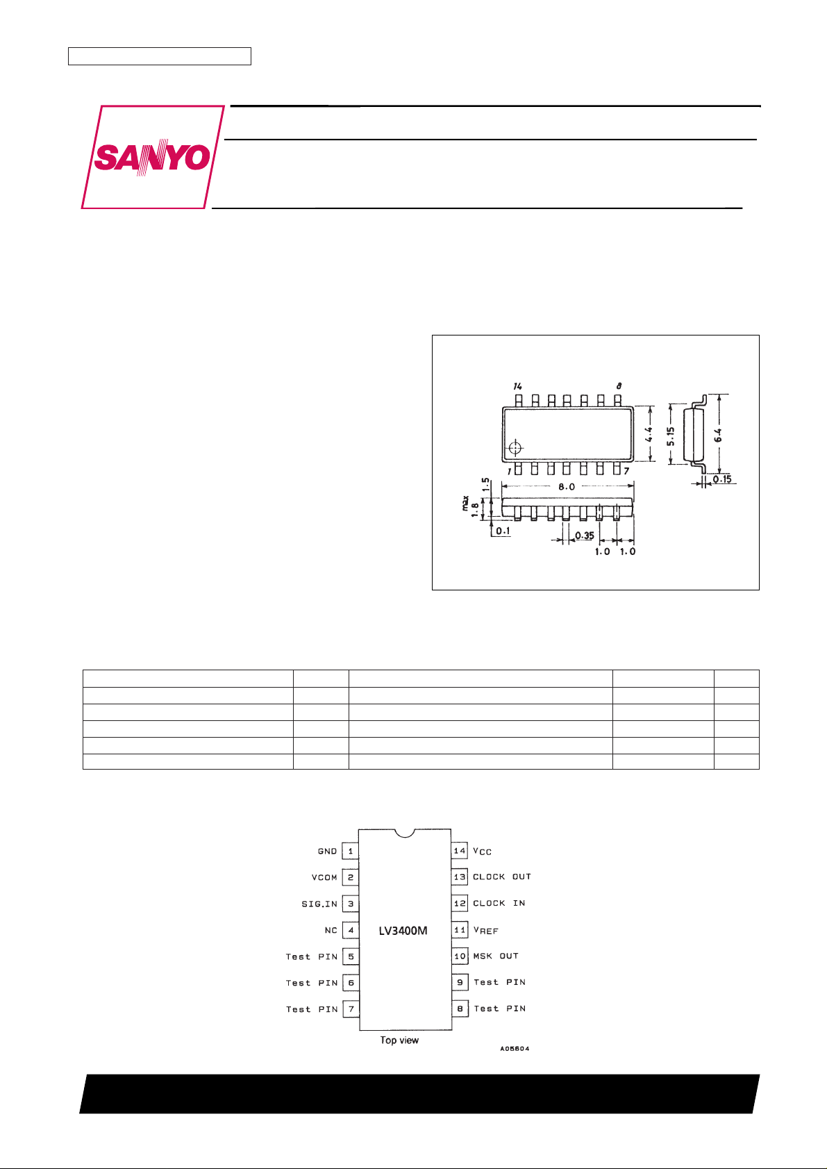
Package Dimensions
unit: mm
3111-MFP14S
Bi CMOS LSI
13096HA (OT)/91295HA (OT)/83194TH (OT) No. 4862-1/4
SANYO: MFP14S
[LV3400M]
SANYO Electric Co.,Ltd. Semiconductor Bussiness Headquarters
TOKYO OFFICE Tokyo Bldg., 1-10, 1 Chome, Ueno, Taito-ku, TOKYO, 110 JAPAN
FM Multiplex Filter
LV3400M
Ordering number : EN4862C
Specifications
Absolute Maximum Ratings at Ta = 25°C
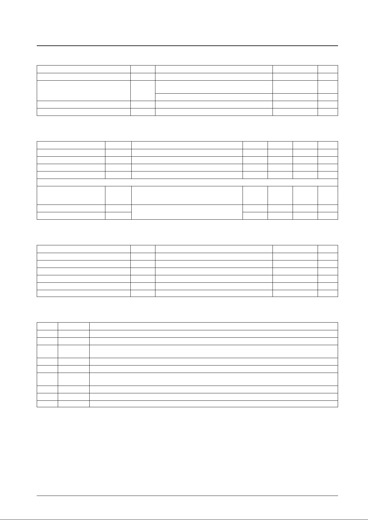
Pin Assignment
Parameter Symbol Conditions Ratings Unit
Maximum supply voltage V
CC
max 6V
Maximum input voltage V
3
, V7, V
12
–0.3 to VCC+ 0.3 V
Allowable power dissipation Pd max 180 mW
Operating temperature Topr –40 to +85 °C
Storage temperature Tstg –55 to +125 °C
No. 4862-2/4
LV3400M
Operating Conditions at Ta = 25°C
Operating Characteristics at Ta = 25°C, VCC= 5 V, fCK= 3.6 MHz, VCK= 1 Vp-p
Reference Characteristics
Pin Functions
Usage Notes
1. Pins 4 to 9 and pin 13 are left open in normal use.
2. The clock should be taken from the decoder (LC72700) clock output pin and input to pin through a capacitor of about
100 pF. Spurious radiation from the clock line can be reduced by inserting a resistor in the line and thus smoothing
the rising and falling edges. This signal is then input to pin 12 through a capacitor.
Parameter Symbol Conditions Ratings Unit
Operating supply voltage range V
CC
4.5 to 5.5 V
A composite signal corresponding to a 100%
200 to 300 mVrms
Input signal voltage range V
IN
FM modulation level
f
IN
= 76 kHz, CW 8 to 30 mVrms
Clock frequency f
CK
3.60 MHz
Clock input voltage V
CK
1.0 to V
CC
Vp-p
Parameter Symbol Conditions min typ max Unit
Current drain I
CCO
The pin 14 current for a no-signal input to V
IN
3.8 6 8 mA
SCF block common voltage V
2
The pin 2 voltage for a no-signal input to V
IN
2.1 2.3 2.5 V
Signal input resistance Rin3 The pin 3 input resistance 36 kΩ
Clock input resistance Rin12 The pin 12 input resistance 100 kΩ
[MSK Output]
The input level such that an MSK output with the same
MSK input sensitivity V
3S
frequency is acquired when a 76-kHz CW is applied 4 mVrms
as V
IN
.
MSK output high level V
10H
VIN= 76 kHz, 4 mVrms, CW
4 V
MSK output low level V
10L
0.4 V
Parameter Symbol Conditions Ratings Unit
AAF cutoff frequency 300 kHz
HPF corner frequency 54 kHz
LPF cutoff frequency 125 kHz
BPF center frequency 76 kHz
BPF -3 dB frequency 19 kHz
Maximum in-band group delay time difference ±5 µs
PinNo. Symbol Description
1 GND Ground
2 VCOM SCF block common. A decoupling capacitor must be used.
3 SIG. IN
Signal input. Input an FM modulated signal (composite signal). A modulated signal between 200 and 300 mVrms should be
input. The input sensitivity for a pure 76-kHz signal is 4 mVrms or lower.
10 MSK OUT MSK output (CMOS output)
11 V
REF
Limiter reference voltage. A low-pass filter is formed by the internal resistance (which is about 10 kΩ) and an external capacitor.
12 CLK IN
3.6-MHz clock input. The DC bias at the CMOS inverter input, to which a 100-kΩ feedback resistor is connected, is about
V
CC
/2. The clock signal is input through a capacitor.
13 CLK OUT The clock output that was wave-shaped by an inverter. This pin is normally left open.
14 V
CC
Power supply
4 to 9 NC, Test PIN This pin must be left open.
 Loading...